EP1280187A2 - Dispositif de fabrication de semiconducteurs ayant un mécanisme tampon et méthode pour mise en tampon de plaquettes semiconductrices - Google Patents
Dispositif de fabrication de semiconducteurs ayant un mécanisme tampon et méthode pour mise en tampon de plaquettes semiconductrices Download PDFInfo
- Publication number
- EP1280187A2 EP1280187A2 EP02255157A EP02255157A EP1280187A2 EP 1280187 A2 EP1280187 A2 EP 1280187A2 EP 02255157 A EP02255157 A EP 02255157A EP 02255157 A EP02255157 A EP 02255157A EP 1280187 A2 EP1280187 A2 EP 1280187A2
- Authority
- EP
- European Patent Office
- Prior art keywords
- wafer
- susceptor
- semiconductor wafer
- reactor
- transferring
- Prior art date
- Legal status (The legal status is an assumption and is not a legal conclusion. Google has not performed a legal analysis and makes no representation as to the accuracy of the status listed.)
- Withdrawn
Links
Images

Classifications
-
- H—ELECTRICITY
- H10—SEMICONDUCTOR DEVICES; ELECTRIC SOLID-STATE DEVICES NOT OTHERWISE PROVIDED FOR
- H10P—GENERIC PROCESSES OR APPARATUS FOR THE MANUFACTURE OR TREATMENT OF DEVICES COVERED BY CLASS H10
- H10P72/00—Handling or holding of wafers, substrates or devices during manufacture or treatment thereof
- H10P72/50—Handling or holding of wafers, substrates or devices during manufacture or treatment thereof for positioning, orientation or alignment
-
- H—ELECTRICITY
- H10—SEMICONDUCTOR DEVICES; ELECTRIC SOLID-STATE DEVICES NOT OTHERWISE PROVIDED FOR
- H10P—GENERIC PROCESSES OR APPARATUS FOR THE MANUFACTURE OR TREATMENT OF DEVICES COVERED BY CLASS H10
- H10P72/00—Handling or holding of wafers, substrates or devices during manufacture or treatment thereof
- H10P72/30—Handling or holding of wafers, substrates or devices during manufacture or treatment thereof for conveying, e.g. between different workstations
- H10P72/33—Handling or holding of wafers, substrates or devices during manufacture or treatment thereof for conveying, e.g. between different workstations into and out of processing chamber
- H10P72/3304—Handling or holding of wafers, substrates or devices during manufacture or treatment thereof for conveying, e.g. between different workstations into and out of processing chamber characterised by movements or sequence of movements of transfer devices
-
- H—ELECTRICITY
- H10—SEMICONDUCTOR DEVICES; ELECTRIC SOLID-STATE DEVICES NOT OTHERWISE PROVIDED FOR
- H10P—GENERIC PROCESSES OR APPARATUS FOR THE MANUFACTURE OR TREATMENT OF DEVICES COVERED BY CLASS H10
- H10P72/00—Handling or holding of wafers, substrates or devices during manufacture or treatment thereof
- H10P72/70—Handling or holding of wafers, substrates or devices during manufacture or treatment thereof for supporting or gripping
- H10P72/76—Handling or holding of wafers, substrates or devices during manufacture or treatment thereof for supporting or gripping using mechanical means, e.g. clamps or pinches
- H10P72/7604—Handling or holding of wafers, substrates or devices during manufacture or treatment thereof for supporting or gripping using mechanical means, e.g. clamps or pinches the wafers being placed on a susceptor, stage or support
- H10P72/7612—Handling or holding of wafers, substrates or devices during manufacture or treatment thereof for supporting or gripping using mechanical means, e.g. clamps or pinches the wafers being placed on a susceptor, stage or support characterised by lifting arrangements, e.g. lift pins
-
- Y—GENERAL TAGGING OF NEW TECHNOLOGICAL DEVELOPMENTS; GENERAL TAGGING OF CROSS-SECTIONAL TECHNOLOGIES SPANNING OVER SEVERAL SECTIONS OF THE IPC; TECHNICAL SUBJECTS COVERED BY FORMER USPC CROSS-REFERENCE ART COLLECTIONS [XRACs] AND DIGESTS
- Y10—TECHNICAL SUBJECTS COVERED BY FORMER USPC
- Y10S—TECHNICAL SUBJECTS COVERED BY FORMER USPC CROSS-REFERENCE ART COLLECTIONS [XRACs] AND DIGESTS
- Y10S414/00—Material or article handling
- Y10S414/135—Associated with semiconductor wafer handling
- Y10S414/141—Associated with semiconductor wafer handling includes means for gripping wafer
Definitions
- the present invention relates to a semiconductor-manufacturing device using a vacuum load-lock system, and the invention particularly relates to a semiconductor-manufacturing device comprising a reactor having a buffer mechanism and its method for buffering semiconductor substrates.
- chambers of a semiconductor-manufacturing device using a vacuum load-lock system which is used for manufacturing conventional semiconductor integrated circuits, comprise a load-lock chamber, a transfer chamber and multiple reactors (process chambers) connected to the transfer chamber.
- a wafer transfer robot is used for supplying wafers automatically.
- the semiconductor-manufacturing device using a vacuum load-lock system operates in the following manner: First, an atmospheric robot carries a wafer from a cassette or a front opening unified pod ("FOUP", e.g., a box possessing detachable cassettes and a front opening interface) into a load-lock chamber.
- FOUP front opening unified pod
- the wafer After evacuating air from the load-lock chamber, the wafer is transferred to each reactor by a vacuum robot provided inside a common polygonal transfer chamber. Wafers for which processing in the reactor is finished, are transferred into the load-lock chamber by the vacuum robot. Finally, after inside the load-lock chamber is restored to atmospheric pressure, processed wafers are transferred to the cassette or the FOUP by an atmospheric robot.
- Such devices are generally called "cluster tools”.
- cluster tools have a single-wafer-processing type and a batch wafer-processing type.
- the single-wafer-processing type is a type in which a single wafer is processed by each reactor.
- the batch wafer-processing type is a type in which multiple wafers are processed by a single reactor.
- productivity is high because multiple wafers are processed by a single reactor.
- batch processing the occurrence of non-uniformity of film thickness and film quality of a thin film formed on a wafer frequently becomes a problem.
- using a single-wafer-processing type wafer processing device is effective.
- the number of reactors increases, a footprint (device space required) and a faceprint (the panel width of a device front) increase, and costs run up. This is because the device has a common polygonal transfer room and reactors are attached to it radially. Additionally, due to the increase in the number of reactors, output significantly drops if operation discontinues due to device breakdowns or maintenance.
- an aim of the present invention is to provide a semiconductor-manufacturing device that realizes low costs, a small footprint and a small faceprint.
- Another aim of the present invention is to provide a semiconductor-manufacturing device that realizes stable processes and high throughput.
- the semiconductor-manufacturing device comprises the following means:
- the present invention provides a buffer mechanism for keeping a semiconductor wafer standing by inside a reactor, comprising: (i) at least two supports for supporting the semiconductor wafer, which are disposed around a susceptor provided in the reactor and which rotate in a horizontal direction; (ii) one shaft each for supporting each support in a vertical direction; (iii) a rotating mechanism for rotating each support coupled to the shaft; and (iv) an elevating mechanism for elevating and descending each shaft.
- each support may have an inner edge curved along a circumference of the semiconductor wafer to line-contact the back of the semiconductor wafer, although any suitable shape (e.g., a triangle, a circle, a rectangle, etc.) can be used as long as the support can support the wafer.
- the rotating mechanism may be a rotary actuator operated electrically or by air pressure.
- the elevating mechanism may be a cylinder mechanism operated electrically or by air pressure.
- the buffer mechanism may further comprise bellows wherein the shaft is provided with the bellows and coupled to the elevating mechanism.
- the buffer mechanism may further comprise an O-ring, wherein the shaft is coupled to the rotating mechanism and sealed by the O-ring.
- the O-ring may comprise a resin seal such as a lip seal or Teflon®.
- the present invention provides a single-wafer-processing reactor comprising: (A) a susceptor for placing a semiconductor wafer thereon, said susceptor being movable upward and downward; (B) a gate valve, through which a transferring arm extends into and retracts from an interior of the reactor; (C) wafer lift pins for lifting the semiconductor wafer, said wafer lift pins being provided in the susceptor at positions where the wafer lift pins do not interfere with movement of the transferring arm, said wafer lift pins being movable upward and downward independently of movement of the susceptor; and (D) the buffer mechanism described above.
- the present invention provides a semiconductor-manufacturing device comprising: (a) the reactor described above; (b) a load-lock chamber connected to the reactor through the gate valve; and (c) a transferring arm for transferring a semiconductor wafer between the reactor and the load-lock chamber through the gate valve.
- the present invention can be applied equally to a method for buffering a semiconductor wafer in a reactor, wherein a wafer is loaded in or unloaded from the reactor at a loading position.
- the method may comprises: (i) supporting a first wafer on wafer lift pins provided in a susceptor provided in the reactor; (ii) placing supports provided around the susceptor between the susceptor and the first wafer on the wafer lift pins; (iii) rotating the supports toward the inside of the susceptor; (iv) elevating the supports to support the first wafer at a stand-by position which is higher than the loading position; (v) loading a second wafer on the susceptor while the first wafer is at the stand-by position; (vi) descending the wafer lift pins to descend the first wafer; and (vii) unloading the first wafer from the reactor.
- the above method may include a method for buffering a processed semiconductor wafer in a reactor, wherein a semiconductor wafer is transferred into or out of the reactor at a transferring position while a susceptor is at an initial position, and a semiconductor wafer is processed at a processing position.
- the method comprises: (A) descending the susceptor from the processing position to the initial position while wafer lift pins remain elevated to support a processed semiconductor wafer on the wafer lift pins after processing is complete; (B) placing at least two supports provided around the susceptor between the susceptor and the semiconductor wafer on the wafer lift pins; (C) rotating the supports toward the inside of the susceptor; (D) elevating the supports to support the semiconductor wafer at a stand-by position which is higher than the transferring position; (E) descending the wafer lift pins to a position lower than the transferring position; (F) transferring an unprocessed semiconductor wafer from a load-lock chamber to the transferring position over the susceptor by a transferring arm; (G) elevating the wafer lift pins to support the unprocessed semiconductor wafer detached from the transferring arm; (H) retracting the transferring arm inside the load-lock chamber; (I) descending the wafer lift pins to descend the unprocessed semiconductor wafer below the transferring position
- a semiconductor wafer is buffered in a reactor, wherein a wafer is loaded in or unloaded from the reactor at a loading position.
- the method comprises: (i) supporting a first wafer at the loading position above a second wafer placed on a susceptor provided in the reactor; (ii) placing supports provided around the susceptor between the susceptor and the first wafer at the loading position; (iii) rotating the supports toward the inside of the susceptor; (iv) elevating the supports to support the first wafer at a stand-by position which is higher than the loading position; and (v) unloading the second wafer from the reactor.
- the above method may include a method for buffering an unprocessed semiconductor wafer in a reactor wherein a semiconductor wafer is transferred into or out of the reactor at a transferring position while a susceptor is at an initial position, and a semiconductor wafer is processed at a processing position, said method comprising: (Al) descending the susceptor together with wafer lift pins at the initial position after processing is complete, on which a processed semiconductor wafer is placed; (B) transferring an unprocessed semiconductor wafer from a load-lock chamber into the reactor at the transferring position by the transferring arm; (C) rotating supports provided around a susceptor toward the inside of the susceptor, said supports being positioned between the susceptor and the unprocessed semiconductor wafer on the transferring arm; (D) elevating the supports to support the unprocessed semiconductor wafer at a stand-by position which is higher than the transferring position; (E) retracting the transferring arm inside the load-lock chamber; (F) elevating the wafer lift pins to elevate
- buffering means temporarily suspending a processed or unprocessed substrate in a reactor while another substrate is transferred into or out of the reactor.
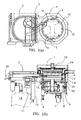
- FIG. 1 shows the best mode for carrying out the compact single-wafer-processing type semiconductor-manufacturing device for forming a thin film on a semiconductor wafer according to the present invention.
- FIG. 1(a) is a plan view of the device.
- FIG. 1(b) is a side view of the device.
- the best mode for carrying out the semiconductor-manufacturing device comprises a reactor 1 for growing a film on a semiconductor wafer, a load-lock chamber 2 for keeping a semiconductor wafer 12 standing by in vacuum, which the load-lock chamber 2 is directly connected to the reactor 1 through a gate valve 13, and a wafer-transferring arm 3 provided inside the load-lock chamber 2, which is a wafer-transferring arm having one thin link-type arm shaft for transferring the semiconductor wafer 12 into the reactor 1.
- a susceptor 14, on which the semiconductor wafer 12 is placed, and a shower plate 19 for equally emitting a jet of reaction gas to the semiconductor wafer 12 are provided.
- the susceptor 14 and the shower plate 19 together comprise high-frequency power electrodes.
- At least three wafer lift pins 15 attached at even intervals pass right through the susceptor vertically.
- the wafer lift pins 15 can move up and down by a cylinder 6.
- the buffer mechanism concerned has at least 2 (e.g., 2, 3, or 4) supporting means (4, 5) for supporting the semiconductor wafer 12, which are provided around the susceptor 14 and which rotate in a horizontal direction. Rotations of the supporting means are synchronized, and only when buffering the semiconductor wafer, the supporting means rotate toward the inside of the susceptor 14 to support the wafer.
- the supporting means (4, 5) comprise preferably a thin plate material of 2mm to 5mm in width.
- the shape of the supporting means (4, 5) is not limited as long as the shape can support the wafer 12 stably. If the contact area of the supporting means with the wafer is large, it causes contamination.
- the shape of a portion of the supporting means (4, 5), which contacts the back side of the wafer is a shape curving along the circumference so that the portion line-contacts the back side of the wafer.
- a material used for the supporting means (4, 5) to avoid contamination, ceramics or aluminum is preferable.
- Each of the supporting means (4, 5) is coupled to the upper end of a shaft means 17 and is supported vertically.
- the lower end of the shaft means 17 is coupled to a rotary actuator 9, and the supporting means is rotated by the rotary actuator.
- the shaft means 17 and the rotary actuator 9 are isolated from the outside by bellows 10.
- the shaft means 17 is sealed preferably by an O-ring 16.
- the rotary actuator 9 can be operated electrically or by air pressure.
- a cylinder 8 is dynamically connected to the lower end of the shaft means 17, a cylinder 8 is dynamically connected.
- the cylinder 8 can move the shaft means 17 up and down, and by this, the supporting means (4, 5) move up and down as well.
- the cylinder 8 can be operated electrically or by air pressure.
- the diameter of the shaft means 17 is preferably within the range of 8mm to 16mm. As a material used for the shaft means 17, to avoid contamination, ceramics or aluminum is preferable.
- the semiconductor-manufacturing device shown in FIG. 1 comprises one load-lock chamber and one reactor that is directly connected to the load-lock chamber
- the present invention is not limited to this embodiment.
- the present invention by arranging two units shown in FIG. 1 in parallel and making a load-lock chamber commonly used, it is possible to apply the present invention to a modularized semiconductor-manufacturing device comprising one load-lock chamber and two reactors.
- two wafers can be concurrently transferred to the reactors and wafers can be processed concurrently in two reactors.
- the buffer mechanism according to the present invention can be applied to all semiconductor-manufacturing devices having a any suitable single-wafer-processing type reactor.
- the buffer mechanism also can be applied to any suitable single-wafer-processing type semiconductor-manufacturing devices (e.g., Eagle 10TM manufactured by Japan ASM) in which a load-lock chamber and a reactor are connected through a transfer chamber.
- suitable single-wafer-processing type semiconductor-manufacturing devices e.g., Eagle 10TM manufactured by Japan ASM
- an atmospheric robot (not shown) carries a semiconductor wafer 12 from a cassette or a FOUP (not shown) into respective load-lock chambers 2 through a flapper valve 20.
- the flapper valve 20 is closed, and air is evacuated from the load-lock chamber 2 by a dry pump 18.
- a gate valve 13 is opened, a wafer transferring arm 3 having a thin-link type arm extends by a rotary actuator 11, and the semiconductor wafer 12 is transferred onto a susceptor 14 inside the reactor 1.
- the wafer transferring arm 3 comprising a link-type arm only reciprocates between the load-lock chamber 2 and the reactor 1 in a straight-line direction, only mechanical positioning adjustment is required and no complicate teaching is required.
- a substrate lift pins 15 protrude from the surface of the susceptor 14 to support the semiconductor wafer 12.
- the wafer transferring arm 3 is placed inside the load-lock chamber 2, and the gate valve 13 is closed.
- the susceptor 14 goes up by a susceptor drive motor 7, and the semiconductor wafer 12 is placed on the surface of the susceptor 14. After that, thin-film deposition processing onto the semiconductor wafer 12 begins. After the thin-film deposition processing is finished, the processed semiconductor wafer is transferred to he cassette or the FOUP by tracking back the order of the operation sequence inversely this time.
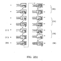
- FIG. 2(a) shows an operation sequence when buffering a processed wafer.
- FIG. 2(b) shows schematic diagrams of reactor operations.
- a susceptor 14 is lowered (Process I).
- the supporting means (4, 5) of the buffer mechanism are raised and stand by, holding the processed wafer.
- the wafer lift pins 15 go down to the position of the susceptor, a transferring arm 3 extends from a load-lock chamber 2 and transfers an unprocessed semiconductor wafer onto the susceptor (Process III).
- FIG. 3 shows an operation sequence when buffering an unprocessed wafer.
- the gate valve 13 is opened, an unprocessed semiconductor wafer 12 is transferred into the reactor 1 by the transferring arm 3, and the supporting means (4, 5) of the buffer mechanism rotate toward the inside of the susceptor 14 (Process II').
- the supporting means (4, 5) of the buffer mechanism go up and stand by, holding the unprocessed semiconductor wafer, and the transferring arm returns into the load-lock chamber (Process III').
- the wafer lift pins 15 are raised, and the transferring arm extends inside the reactor again (Process IV').
- the wafer lift pins 15 are lowered, and the transferring arm receives a processed semiconductor wafer and returns inside the load-lock chamber 2 (Process V').
- the wafer lift pins go up, the gate valve is closed, the supporting means (4, 5) of the buffer mechanism go down, the wafer lift pins receive the unprocessed semiconductor wafer, and the supporting means (4, 5) of the buffer mechanism rotate toward the outside of the susceptor (Process VI').
- the susceptor 14 is raised, and vapor deposition of the semiconductor wafer is performed (Process VII'). After this, this operating sequence is repeated.
- the present invention includes the following embodiments:
- a semiconductor-manufacturing device comprises a single-wafer-processing type reactor comprising a buffer mechanism for keeping a semiconductor wafer standing by inside the reactor.
- the buffer mechanism comprises at least two supporting means, which are provided around a susceptor to support the semiconductor wafer and which rotate in a horizontal direction, a shaft means for supporting each supporting means in a vertical direction, a rotating mechanism for rotating each supporting means coupled to the shaft means, and an elevating means for moving each shaft means up and down.
- a method for buffering a processed semiconductor wafer using the buffer mechanism comprises (I) a process in which the susceptor is lowered with wafer lift pins being raised after processing is finished, (II) a process in which the supporting means of the buffer mechanism are arranged between the under surface of the semiconductor wafer and the susceptor, are rotated to inside the susceptor, and move upwards to stand by for supporting the semiconductor wafer, (III) a process in which the wafer lift pins are lowered to the position of the susceptor and an unprocessed semiconductor wafer is transferred from a load-lock chamber onto the susceptor by a transferring arm, (IV) a process in which the transferring arm returns inside the load-lock chamber while the wafer lift pins go up and hold the unprocessed semiconductor wafer, (V) a process in which the wafer lift pins go down to the position of the susceptor again and the transferring arm is inserted in the reactor, (VI) a process in which the supporting means of the buffer mechanism go down and the processed wa
- a method for buffering an unprocessed semiconductor wafer using the buffer mechanism comprises
- the buffer mechanism By the buffer mechanism according to the present invention, by keeping a processed or unprocessed wafer standing by inside the reactor, a processed wafer and an unprocessed wafer inside the load-lock chamber can be switched. In doing so, despite the configuration having one transferring arm per reactor, a device with ability equivalent to that with double arms was able to be achieved. Consequently, the problem caused by the transfer rate-limiting factors is solved and a semiconductor-manufacturing device realizing stable processes and high throughput can be realized.
- a load-lock chamber can be reduced as compared with a conventional device with double arms, a semiconductor-manufacturing device realizing low costs, a small footprint and a small faceprint can be provided.
Landscapes
- Container, Conveyance, Adherence, Positioning, Of Wafer (AREA)
- Crystals, And After-Treatments Of Crystals (AREA)
Applications Claiming Priority (2)
| Application Number | Priority Date | Filing Date | Title |
|---|---|---|---|
| JP2001222962 | 2001-07-24 | ||
| JP2001222962A JP2003037146A (ja) | 2001-07-24 | 2001-07-24 | バッファ機構を有する半導体製造装置及び方法 |
Publications (2)
| Publication Number | Publication Date |
|---|---|
| EP1280187A2 true EP1280187A2 (fr) | 2003-01-29 |
| EP1280187A3 EP1280187A3 (fr) | 2007-01-24 |
Family
ID=19056367
Family Applications (1)
| Application Number | Title | Priority Date | Filing Date |
|---|---|---|---|
| EP02255157A Withdrawn EP1280187A3 (fr) | 2001-07-24 | 2002-07-23 | Dispositif de fabrication de semiconducteurs ayant un mécanisme tampon et méthode pour mise en tampon de plaquettes semiconductrices |
Country Status (4)
| Country | Link |
|---|---|
| US (1) | US6860711B2 (fr) |
| EP (1) | EP1280187A3 (fr) |
| JP (1) | JP2003037146A (fr) |
| KR (1) | KR100873967B1 (fr) |
Families Citing this family (10)
| Publication number | Priority date | Publication date | Assignee | Title |
|---|---|---|---|---|
| JP4417669B2 (ja) * | 2003-07-28 | 2010-02-17 | 日本エー・エス・エム株式会社 | 半導体処理装置および半導体ウエハーの導入方法 |
| US7477956B2 (en) * | 2004-07-12 | 2009-01-13 | Applied Materials, Inc. | Methods and apparatus for enhancing electronic device manufacturing throughput |
| US20070077134A1 (en) * | 2005-09-30 | 2007-04-05 | Dickinson Colin J | Vacuum handler systems and processes for flexible automation of semiconductor fabrication |
| US7690881B2 (en) * | 2006-08-30 | 2010-04-06 | Asm Japan K.K. | Substrate-processing apparatus with buffer mechanism and substrate-transferring apparatus |
| WO2009055612A1 (fr) | 2007-10-27 | 2009-04-30 | Applied Materials, Inc. | Porte-substrats scellés et systèmes et procédés pour transporter des substrats |
| US20090162170A1 (en) * | 2007-12-19 | 2009-06-25 | Asm Japan K.K. | Tandem type semiconductor-processing apparatus |
| JP5675416B2 (ja) * | 2011-02-17 | 2015-02-25 | 東京エレクトロン株式会社 | 被処理体の搬送方法及び被処理体処理装置 |
| JP7030416B2 (ja) * | 2017-03-16 | 2022-03-07 | キヤノン株式会社 | 基板保持装置、リソグラフィ装置、物品の製造方法 |
| CN110931410A (zh) * | 2019-12-02 | 2020-03-27 | 浙江求是半导体设备有限公司 | 一种用于反应室的晶片传动装置和传动方法 |
| US11569102B2 (en) | 2020-02-14 | 2023-01-31 | Applied Materials, Inc. | Oxidation inhibiting gas in a manufacturing system |
Family Cites Families (13)
| Publication number | Priority date | Publication date | Assignee | Title |
|---|---|---|---|---|
| US5643366A (en) * | 1994-01-31 | 1997-07-01 | Applied Materials, Inc. | Wafer handling within a vacuum chamber using vacuum |
| US5730801A (en) * | 1994-08-23 | 1998-03-24 | Applied Materials, Inc. | Compartnetalized substrate processing chamber |
| US6102164A (en) * | 1996-02-28 | 2000-08-15 | Applied Materials, Inc. | Multiple independent robot assembly and apparatus for processing and transferring semiconductor wafers |
| US5848670A (en) * | 1996-12-04 | 1998-12-15 | Applied Materials, Inc. | Lift pin guidance apparatus |
| US6575737B1 (en) * | 1997-06-04 | 2003-06-10 | Applied Materials, Inc. | Method and apparatus for improved substrate handling |
| JPH11288995A (ja) * | 1998-04-04 | 1999-10-19 | Tokyo Electron Ltd | 搬送システム及び処理装置 |
| JP3661138B2 (ja) * | 1998-04-04 | 2005-06-15 | 東京エレクトロン株式会社 | アライメント高速処理機構 |
| JP2000040728A (ja) * | 1998-07-22 | 2000-02-08 | Nippon Asm Kk | ウェハ搬送機構 |
| US6168668B1 (en) * | 1998-11-25 | 2001-01-02 | Applied Materials, Inc. | Shadow ring and guide for supporting the shadow ring in a chamber |
| KR100551806B1 (ko) * | 1999-09-06 | 2006-02-13 | 동경 엘렉트론 주식회사 | 반도체 처리용 반송 장치 및 수용 장치와, 반도체 처리시스템 |
| JP4607301B2 (ja) * | 1999-09-06 | 2011-01-05 | 東京エレクトロン株式会社 | 半導体処理用の搬送装置及び半導体処理システム |
| US6630053B2 (en) * | 2000-08-22 | 2003-10-07 | Asm Japan K.K. | Semiconductor processing module and apparatus |
| US6485248B1 (en) * | 2000-10-10 | 2002-11-26 | Applied Materials, Inc. | Multiple wafer lift apparatus and associated method |
-
2001
- 2001-07-24 JP JP2001222962A patent/JP2003037146A/ja active Pending
-
2002
- 2002-07-01 US US10/187,670 patent/US6860711B2/en not_active Expired - Lifetime
- 2002-07-23 KR KR1020020043319A patent/KR100873967B1/ko not_active Expired - Lifetime
- 2002-07-23 EP EP02255157A patent/EP1280187A3/fr not_active Withdrawn
Also Published As
| Publication number | Publication date |
|---|---|
| US6860711B2 (en) | 2005-03-01 |
| KR100873967B1 (ko) | 2008-12-12 |
| KR20030010500A (ko) | 2003-02-05 |
| JP2003037146A (ja) | 2003-02-07 |
| EP1280187A3 (fr) | 2007-01-24 |
| US20030021657A1 (en) | 2003-01-30 |
Similar Documents
| Publication | Publication Date | Title |
|---|---|---|
| US7690881B2 (en) | Substrate-processing apparatus with buffer mechanism and substrate-transferring apparatus | |
| KR100310249B1 (ko) | 기판처리장치 | |
| KR100789461B1 (ko) | 반도체처리모듈과 장치 | |
| US6676761B2 (en) | Method and apparatus for dechucking a substrate | |
| US6225233B1 (en) | Semiconductor device manufacturing machine and method for manufacturing a semiconductor device by using THE same manufacturing machine | |
| KR100269097B1 (ko) | 기판처리장치 | |
| JP5548163B2 (ja) | 基板搬送機構、基板処理装置および半導体装置の製造方法 | |
| WO2003071600A1 (fr) | Mecanisme de transport pour substrats, utilise dans un systeme de traitement de semi-conducteurs | |
| KR20230017322A (ko) | 고온 및 진공 격리 프로세싱 미니 환경들 | |
| US6860711B2 (en) | Semiconductor-manufacturing device having buffer mechanism and method for buffering semiconductor wafers | |
| US20070215049A1 (en) | Transfer of wafers with edge grip | |
| CN201274284Y (zh) | 真空腔室和具有该真空腔室的基板传送系统 | |
| JPH10107124A (ja) | 基板処理装置 | |
| KR20100093994A (ko) | 기판처리시스템 | |
| WO2010013333A1 (fr) | Dispositif sous vide et procédé de traitement sous vide | |
| JP2004119627A (ja) | 半導体製造装置 | |
| JP4270413B2 (ja) | プロセス装置 | |
| JP7630295B2 (ja) | プラズマ処理用載置部、およびプラズマ処理装置 | |
| JP2003060009A (ja) | 基板処理装置および基板処理方法 | |
| JP5010620B2 (ja) | プロセス装置 | |
| KR20230173245A (ko) | 반도체 제조용 부품 캐리어 및 이를 이용한 반도체 제조용 부품 반송장치 | |
| KR20230011137A (ko) | 리프트 어셈블리 및 그를 포함하는 반도체 소자의 제조 장치 | |
| WO2000024047A1 (fr) | Appareil de fabrication de semiconducteurs | |
| JP2004193217A (ja) | 基材搬送装置および基材処理装置 |
Legal Events
| Date | Code | Title | Description |
|---|---|---|---|
| PUAI | Public reference made under article 153(3) epc to a published international application that has entered the european phase |
Free format text: ORIGINAL CODE: 0009012 |
|
| AK | Designated contracting states |
Designated state(s): AT BE BG CH CY CZ DE DK EE ES FI FR GB GR IE IT LI LU MC NL PT SE SK TR |
|
| AX | Request for extension of the european patent |
Extension state: AL LT LV MK RO SI |
|
| PUAL | Search report despatched |
Free format text: ORIGINAL CODE: 0009013 |
|
| AK | Designated contracting states |
Kind code of ref document: A3 Designated state(s): AT BE BG CH CY CZ DE DK EE ES FI FR GB GR IE IT LI LU MC NL PT SE SK TR |
|
| AX | Request for extension of the european patent |
Extension state: AL LT LV MK RO SI |
|
| AKX | Designation fees paid | ||
| REG | Reference to a national code |
Ref country code: DE Ref legal event code: 8566 |
|
| STAA | Information on the status of an ep patent application or granted ep patent |
Free format text: STATUS: THE APPLICATION IS DEEMED TO BE WITHDRAWN |
|
| 18D | Application deemed to be withdrawn |
Effective date: 20070725 |