EP1280232A1 - Zur gemeinsamen Nutzung bei mehreren Frequenzen geeignete Antennenvorrichtung und elektronisches Gerät mit dieser - Google Patents
Zur gemeinsamen Nutzung bei mehreren Frequenzen geeignete Antennenvorrichtung und elektronisches Gerät mit dieser Download PDFInfo
- Publication number
- EP1280232A1 EP1280232A1 EP02016766A EP02016766A EP1280232A1 EP 1280232 A1 EP1280232 A1 EP 1280232A1 EP 02016766 A EP02016766 A EP 02016766A EP 02016766 A EP02016766 A EP 02016766A EP 1280232 A1 EP1280232 A1 EP 1280232A1
- Authority
- EP
- European Patent Office
- Prior art keywords
- antenna device
- conductor
- antenna
- length
- resonant frequency
- Prior art date
- Legal status (The legal status is an assumption and is not a legal conclusion. Google has not performed a legal analysis and makes no representation as to the accuracy of the status listed.)
- Ceased
Links
- 239000004020 conductor Substances 0.000 claims abstract description 52
- 239000000758 substrate Substances 0.000 claims description 8
- 230000000295 complement effect Effects 0.000 claims description 3
- 230000000694 effects Effects 0.000 description 5
- 230000001939 inductive effect Effects 0.000 description 5
- 230000003071 parasitic effect Effects 0.000 description 5
- 230000005855 radiation Effects 0.000 description 4
- 239000002184 metal Substances 0.000 description 3
- 239000011295 pitch Substances 0.000 description 2
- 230000005404 monopole Effects 0.000 description 1
Images






Classifications
-
- H—ELECTRICITY
- H01—ELECTRIC ELEMENTS
- H01Q—ANTENNAS, i.e. RADIO AERIALS
- H01Q9/00—Electrically-short antennas having dimensions not more than twice the operating wavelength and consisting of conductive active radiating elements
- H01Q9/04—Resonant antennas
- H01Q9/30—Resonant antennas with feed to end of elongated active element, e.g. unipole
- H01Q9/42—Resonant antennas with feed to end of elongated active element, e.g. unipole with folded element, the folded parts being spaced apart a small fraction of the operating wavelength
-
- H—ELECTRICITY
- H01—ELECTRIC ELEMENTS
- H01Q—ANTENNAS, i.e. RADIO AERIALS
- H01Q1/00—Details of, or arrangements associated with, antennas
- H01Q1/36—Structural form of radiating elements, e.g. cone, spiral, umbrella; Particular materials used therewith
-
- H—ELECTRICITY
- H01—ELECTRIC ELEMENTS
- H01Q—ANTENNAS, i.e. RADIO AERIALS
- H01Q5/00—Arrangements for simultaneous operation of antennas on two or more different wavebands, e.g. dual-band or multi-band arrangements
- H01Q5/30—Arrangements for providing operation on different wavebands
- H01Q5/307—Individual or coupled radiating elements, each element being fed in an unspecified way
- H01Q5/314—Individual or coupled radiating elements, each element being fed in an unspecified way using frequency dependent circuits or components, e.g. trap circuits or capacitors
- H01Q5/321—Individual or coupled radiating elements, each element being fed in an unspecified way using frequency dependent circuits or components, e.g. trap circuits or capacitors within a radiating element or between connected radiating elements
-
- H—ELECTRICITY
- H01—ELECTRIC ELEMENTS
- H01Q—ANTENNAS, i.e. RADIO AERIALS
- H01Q7/00—Loop antennas with a substantially uniform current distribution around the loop and having a directional radiation pattern in a plane perpendicular to the plane of the loop
-
- H—ELECTRICITY
- H01—ELECTRIC ELEMENTS
- H01Q—ANTENNAS, i.e. RADIO AERIALS
- H01Q9/00—Electrically-short antennas having dimensions not more than twice the operating wavelength and consisting of conductive active radiating elements
- H01Q9/04—Resonant antennas
- H01Q9/0407—Substantially flat resonant element parallel to ground plane, e.g. patch antenna
- H01Q9/0421—Substantially flat resonant element parallel to ground plane, e.g. patch antenna with a shorting wall or a shorting pin at one end of the element
-
- H—ELECTRICITY
- H01—ELECTRIC ELEMENTS
- H01Q—ANTENNAS, i.e. RADIO AERIALS
- H01Q9/00—Electrically-short antennas having dimensions not more than twice the operating wavelength and consisting of conductive active radiating elements
- H01Q9/04—Resonant antennas
- H01Q9/0407—Substantially flat resonant element parallel to ground plane, e.g. patch antenna
- H01Q9/0442—Substantially flat resonant element parallel to ground plane, e.g. patch antenna with particular tuning means
Definitions
- the present invention relates to an antenna device and an electronic equipment having the antenna device, in particular to an antenna device contained in an electronic equipment which can be commonly used at a plurality of frequencies capable of being utilized in a radio communication.
- wireless LANs for example, the Bluetooth system
- Bluetooth system that can be used also in portable type computers
- a computer network in recent years.
- an antenna device for a radio communication used in such a portable type computer the following items are required.
- a multi-frequency operation for example, one frequency band of 2.4 GHz and another frequency band of 5.2 GHz.
- the portable type computer in order that the portable type computer may be responsive to both the frequency bands, it has been conventionally required that the portable type computer has two kinds of antenna devices.
- the portable type computer it is difficult to obtain spaces for mounting the two kinds of antenna device, respectively, since the portable type computer is designed to be as small as possible in size and weight. Accordingly, it is required that even a single antenna device can be responsive to both the frequency bands so that the spaces for mounting the antenna device may be as small as possible in a portable type computer.
- the antenna device can be contained in the portable type computer. Accordingly, it is, of course, required that the antenna device is small in size. In addition, it is further required that the antenna device is not easily influenced electrically from an adjacent housing body, or the like.
- a wire antenna such as a dipole antenna, a monopole antenna, and the like resonates at a frequency of integer times (one, two, three...) as large as a predetermined frequency, in a case that the wire antenna has an antenna-length of approximately ninety-five percentages as long as a wave-length of as half as the predetermined frequency.
- second frequency is not integer times (one, two, three%) as large as first frequency, as mentioned before.
- the conventional antenna device disclosed therein has two dipole antennas resonating at first, second frequency, respectively.
- the two dipole antennas are located in parallel in the same feed line and supplied with electric power transversely.
- the conventional antenna device having two dipole antennas not only a structure of the antenna device inevitably becomes large in size but also a constitution of an impedance matching section becomes complicated. Further, the conventional antenna device having the two dipole antennas is disadvantageous in actual use, since loss is increased in the feeder thereof, and the like.
- an input impedance of a conventional dipole antenna, and the like becomes low almost down to short-circuit impedance near a metal conductor, particularly when an interval between the conventional dipole antenna and the metal conductor is not longer than a wave-length of one-tenth of the predetermined frequency.
- each of the first and the second resonant frequencies comes to a frequency characteristic having a narrow band.
- an antenna device capable of being commonly used at the first and the second frequencies
- a proposal is made about an antenna device in which a parasitic element resonating at the second frequency is additionally located in a dipole antenna resonating at the first frequency.
- disclosure is, respectively, made about an antenna device that a parasitic element consisting of a feed-less element is additionally located near a dipole antenna resonating at the first frequency, so that a resonant characteristic of the second frequency can be obtained in the antenna device.
- the resonant characteristic of the second frequency is obtained in the antenna device by additionally locating the parasitic element, limitation is caused to occur for a position and a size of the parasitic element in the antenna device. Further, the antenna device becomes large in size by a size of the parasitic element.
- the antenna device In view of a radiation characteristic of the dipole antenna, it is necessary for the antenna device to be separated from the adjacent metal conductor, and the like by a distance of a quarter wave-length of the first frequency approximately, and integer times as large as the first frequency in addition thereto. As a result, a space of not smaller than the wave-length of one-fourth of the first frequency is required for mounting the antenna device in the computer.
- an antenna device capable of being contained in a computer by readily obtaining impedance matching between an antenna element and a feeding system thereof, a proposal is made about an antenna device, such as a loop antenna, a folded dipole antenna, and the like, each of which is a wire antenna that an input impedance is increased by folding an antenna element.
- a resonant frequency of the antenna device depends on an antenna length thereof. It is therefore difficult to adjust the second frequency after the first frequency has been adjusted.
- a feature of the present invention is to provide an antenna device which is capable of being commonly used at a multi-frequency operation and being contained in an electronic equipment.
- Another feature of the present invention is to provide an electronic equipment having an antenna device of the type described.
- an antenna device for use in an electronic equipment, comprising: a first conductor having an electrically half wave-length of a first resonant frequency; a feed point to which an end of said first conductor is connected; a plate-shaped second conductor on which said feed point is located and on which another end of said first conductor is grounded; and an impedance element which is loaded on said first conductor and which varies at least one of said first resonant frequency and a second resonant frequency.
- the impedance element may vary said first resonant frequency.
- the impedance element may vary said second resonant frequency.
- the impedance element may vary both said first resonant frequency and said second resonant frequency.
- the first conductor may be formed to be semi-rectangular.
- the first conductor may be line-shaped.
- the first conductor may be belt-shaped.
- the first conductor may have a primary portion elongating from said plate-shaped second conductor and a secondary portion other than said primary portion, wherein said primary portion may be formed to have a length between 0.05 and 0.10, both inclusive, of a wave-length of a first resonant frequency.
- the length of said primary portion may be between 0.07 and 0.08, both inclusive, of said wave-length of said first resonant frequency.
- the impedance element may be located on said secondary portion with being offset from a center of said secondary portion towards a side of a portion on which said first conductor is grounded.
- the impedance element may be a lumped capacitance or inductance element.
- the lumped capacitance or inductance element may be formed to be rectangular.
- the first conductor may be formed on a dielectric block having a hexahedron shape.
- the first conductor may be formed on a dielectric substrate.
- the first conductor may be formed on said plate-shaped second conductor as a complement pair structure.
- an electronic equipment including said antenna device, said electronic equipment transmitting information to the outside thereof and receiving information from the outside thereof by a radio communication using said antenna device.
- FIG. 1 is a perspective view for schematically showing an antenna device according to the first embodiment of the present invention.
- the antenna device 10 comprises an antenna element (first conductor) 11, a feed point 12, a conductive plate (second conductor) 13, and an impedance element 14.
- the antenna element 11 is formed to have a shape of a semi-rectangular line. One end of the antenna element 11 is connected to the feed point 12 while another end of the antenna element 11 is grounded on the conductive plate 13 through a ground portion 11a.
- the feed point 12 is located on the conductive plate 13 through an insulating layer (not shown).
- the impedance element 14 is loaded halfway on the antenna element 11.
- Fig. 2 is a perspective view for schematically showing an antenna device according to the second embodiment of the present invention.
- the antenna device 20 according to the second embodiment illustrated in Fig. 2 has a structure basically similar to that of the antenna device 10 illustrated in Fig. 1 except that an antenna element (first conductor) 21 is formed to have a shape of a semi-rectangular belt in the antenna device 20. Similar portions are designated by like reference numerals and explanations thereof are omitted accordingly.
- the antenna device 20 also brings meritorious operations and effects similar to those of the antenna device 10 illustrated in Fig. 1. Besides, description is hereunder made as regards operations and effects of only the antenna device 10 illustrated in Fig. 1, for convenience of explanation.
- the antenna element 11 of the antenna device 10 includes not only portions elongating perpendicularly from the conductive plate 13, namely, a feeding side perpendicular portion 11b and a grounding side perpendicular portion 11c but also a portion other than the perpendicular portions 11b and 11c, namely, a parallel portion 11d.
- the antenna element 11 is formed on a condition that an added value of length (h) of the feeding side perpendicular portion 11b, length (h) of the grounding side perpendicular portion 11c, and length (b) of the parallel portion 11d is electrically a half length (0.5 ⁇ 1 ) of a wave-length of the first resonant frequency (f1).
- the antenna element 11 having such a structure can be considered as depicted in Figs. 3A and 3B, when the impedance element 14 is ignored.
- a loop antenna 1 is composed of both the antenna element 11 and the electrical image thereof to have the perimeter of a wave-length (1 ⁇ ) of the first resonant frequency (f1).
- the antenna element 11 located on the conductive plate 13 becomes equal to a half of the loop antenna 1 formed by setting a conductive plain plate on a central plane perpendicular to a loop plane of the loop antenna 1 including the feed point 2.
- a voltage (V) of the feed point 2 is equivalently divided into a half voltage (V/2) on portions above and under the conductive plain plate, respectively.
- the portions above and under the conductive plain plate each having the half voltage (V/2) are connected in series to each other.
- an input impedance and a radiation resistance of the antenna element 11 located on the conductive plate 13, that is, a half of the loop antenna 1, as mentioned before, become one half of those of the original loop antenna 1.
- a radiation characteristic of the antenna element 11 becomes similar to that of the original loop antenna 1.
- the antenna device 10 can therefore be constituted so that not only an impedance matching between the antenna element 11 and the feed point 12 may be readily obtained but also the size of the antenna device 10 may be made compact without changing the radiation characteristic.
- Fig. 4 is a graph for showing a relation between a normalized by wave length (h) of the feeding side perpendicular portion 11b (the grounding side perpendicular portion 11c) and an input impedance (input resistance) (Rin[ ⁇ ]) in the first and the second frequencies (f1[GHz]), (f2[GHz]), respectively, of the antenna element 11 located on the conductive plate 13.
- h normalized by wave length
- f1[GHz] the feeding side perpendicular portion 11b
- f2[GHz] input impedance
- an impedance matching can be readily obtained at a characteristic impedance (Z0) of 50 [ ⁇ ], when the length (h) of the feeding side perpendicular portion 11b (the grounding side perpendicular portion 11c) is between 0.05 and 0.10, both inclusive, preferably 0.07 and 0.08, both inclusive.
- the reactance element (X1) may be either capacitive (X1 ⁇ 0) and inductive (X1>0).
- the resonant frequency of the antenna device 10 can be made higher by loading the reactance element (X1) capacitive (X1 ⁇ 0).
- the resonant frequency of the antenna device 10 can be made lower by loading the reactance element (X1) inductive (X1>0). Accordingly, the antenna device 10 can obtain resonant characteristic at a desirable frequency with the impedance element 14 being optimized.
- each the length (h) of the feeding side perpendicular portion 11b and the grounding side perpendicular portion 11c is 0.125 ⁇ 1 while the length (b) of the parallel portion 11d is 0.25 ⁇ 1 in the antenna element 11.
- variation of an input impedance (Zin) at the first frequency (f1) becomes large as shown by a dotted line illustrated in Fig.6A, when the reactance element (X1) is inductive (X1>0).
- variation of an input impedance (Rin) at the second frequency (f2) becomes small as shown by an alternate long and two short dash line illustrated in Fig.6A. Accordingly, variation of an input impedance (Xin) becomes gentle as shown by an alternate long and two short dash line illustrated in Fig.6A.
- variation of an input impedance (Zin) at the first frequency (f1) substantially keeps a certain value as shown by an actual line illustrated in Fig.6B, when the reactance element (X1) is capacitive (X1 ⁇ 0).
- variation of an input impedance (Rin) at the second frequency (f2) becomes small as shown by an alternate long and short dash line illustrated in Fig.6B. Accordingly, variation of an input impedance (Xin) becomes large as shown by an alternate long and short dash line illustrated in Fig.6B.
- the impedance element 14 is a lumped capacitance or inductance element
- the impedance element 14 is basically located on the antenna element 11 with the impedance element 14 being perpendicular to a principal surface of the conductive plate 13, as illustrated in Fig. 1.
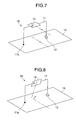
- the impedance element 14 of a lumped capacitance or inductance element may be located on the antenna element 11 with the impedance element 14 being parallel to a principal surface of the conductive plate 13, as illustrated in Fig. 7.
- the impedance element 14 of a lumped capacitance or inductance element may be located on the antenna element 11 with the impedance element 14 being inclined to a principal surface of the conductive plate 13 at a predetermined angle ⁇ , that is, between 0° and 90° (0[° ] ⁇ ⁇ [° ] ⁇ 90[° ]), as illustrated in Fig. 8.
- Figs. 9A through 9D show a relation between the frequency (f[GHz]) and the return loss (RL[dB]), when a distance (Sl), namely, a distance from the feed point 12 to a loading position of the impedance element 14 is varied.
- the second resonant frequency (f2) can be adjustable by loading the reactance element (X1) capacitive (X1 ⁇ 0) between the central position (B)[b/2] and the position (C)[3b/4] near the ground portion 11a.
- Fig. 10 is a perspective view for schematically showing an antenna device according to the third embodiment of the present invention.
- the antenna device 30 comprises an antenna element (first conductor) 31, a feed point 32, a conductive plate (second conductor) 33, an impedance element 34, and a dielectric block 35.
- the antenna element 31 is formed to have a shape of a semi-rectangular line, similarly to the antenna element 11 of the first embodiment.
- the antenna element 31 also includes a ground portion 31a, a feeding side perpendicular portion 31b, a grounding side perpendicular portion 31c, and a parallel portion 31d.
- the feed point 32 is located an end of the conductive plate 33.
- the impedance element 34 is similar to the impedance element 14 of the first embodiment, namely, a capacitance, an inductance, or the like used in an electronic circuit or a lumped capacitance or inductance element composed of an element having certain size and configuration.
- the dielectric block 35 is formed to have a hexahedron shape.
- the antenna element 31 is formed on an upper surface and side surfaces opposite to each other of the dielectric block 35. Namely, the parallel portion 31d of the antenna element 31 is formed on an upper surface of the dielectric block 35 while the feeding side perpendicular portion 31b and the grounding side perpendicular portion 31c are formed on side surfaces of the dielectric block 35.
- the impedance element 34 is formed on the upper surface of the dielectric block 35 to be located halfway on the antenna element 31.
- the dielectric block 35 is mounted on the conductive plate 33.
- the feeding side perpendicular portion 31b is connected to the feed point 32 by way of a feed line formed on the conductive plate 33, for example a microstrip line 33a.
- the grounding side perpendicular portion 31c is grounded on the conductive plate 33 through the ground portion 31a.
- Fig. 11 is a perspective view for schematically showing an antenna device according to the fourth embodiment of the present invention.
- the antenna device 40 according to the fourth embodiment illustrated in Fig. 11 has a structure basically similar to that of the antenna device 30 illustrated in Fig. 10 except that, in spite of the above-mentioned dielectric block 35, the antenna device 40 has a rectangular dielectric substrate 45 having both ends folded substantially perpendicular thereto and that an antenna element (first conductor) 41 and an impedance element 44 are formed on an upper surface and side surfaces opposite to each other of the rectangular dielectric substrate 45. With the structure, the rectangular dielectric substrate 45 is mounted on the conductive plate 43.
- the feeding side perpendicular portion 41b is connected to the feed point 42 by way of a feed line formed on the conductive plate 43, for example a microstrip line 43a.
- the grounding side perpendicular portion 41c is grounded on the conductive plate 43 through the ground portion 41a.
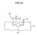
- Fig. 12 is a view for schematically showing an antenna device according to the fifth embodiment of the present invention.
- the antenna device 50 according to the fifth embodiment illustrated in Fig. 12 has, what is called, a complement pair structure.
- the antenna device 50 comprises a conductive plate 53, an antenna element 51 which is composed of a slit having a shape of a semi-rectangular line formed in the conductive plate 53, and the impedance element 54 which is composed of a cut portion formed in the conductive plate 53, as illustrated in Fig. 12.
- the antenna device 50 further comprises a feed point 52.
- the antenna element 51 of a slit includes three slit portions which function as a feeding side perpendicular portion 51b, a grounding side perpendicular portion 51c, and a parallel portion 51d, respectively. Further, the feed point 52 is connected to both edges of the slit portion functioning as the feeding side perpendicular portion 51b.
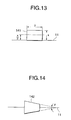
- the impedance element 14 basically has a rectangular configuration having length(x) ⁇ width(y).
- variations of the configuration illustrated in Figs. 13 through 20 can be applied to the impedance element 14 (24, 34, 44, and 54) of a lumped capacitance or inductance element.
- an impedance element 141 has a rectangular configuration which has length(x) ⁇ width(y) and which is offset from the antenna element 11 by a predetermined length (x/2).
- an impedance element 142 illustrated in Fig. 14 has a trapezoidal configuration which has a taper of an angle ( ⁇ ).
- an impedance element 143 illustrated in Fig. 15 has a circular configuration which has a radius of (r).
- an impedance element 144 illustrated in Fig. 16 has a configuration which has a bump including width (w1) and width (w2) as well as length (l1) and length (l2).
- an impedance element 145 illustrated in Fig. 17 is composed of an antenna element 11 itself having a bump including width (w3) and width (w4).
- an impedance element 146 illustrated in Fig. 18 is composed of an antenna element 11 itself cut halfway thereon and having a gap (g) between both the cut portions thereof.
- an impedance element 147 illustrated in Fig. 19A (a plan view) and Fig. 19B (a side view) is composed of an antenna element 11 itself cut halfway thereon and both the cut portions thereof are partially overlapped on each other.
- the impedance element 147 can therefore be realized, for example, by a substrate of a stacked-layer structure.
- an impedance element 148 illustrated in Fig. 20 has a box-like three-dimensional configuration.
- the impedance element 148 can be realized, for example, by folding both ends of a rectangular substrate so that the both ends may be perpendicular to the rectangular substrate.
- the antenna element 11 stands on the principal surface of the conductive plate 13.
- variations of the location illustrated in Figs. 21 through 29 can be applied to the antenna device 10 (20, 30, 40, and 50).
- the antenna element 11 is located on an end of the conductive plate 13 to be elongated horizontally to the principal surface of the conductive plate 13.
- the antenna element 11 is located on the end of the conductive plate 13 to be inclined to the principal surface of the conductive plate 13 at a predetermined angle ⁇ 1, that is, between 0° and 180° (0[° ] ⁇ 1 [° ] ⁇ 180[° ]). Further, in the antenna device 10 illustrated in Fig. 23, the antenna element 11 is located on a corner of the conductive plate 13 to be elongated horizontally to the principal surface of the conductive plate 13 with the antenna element 11 being folded as depicted in Fig. 23. Moreover, in the antenna device 10 illustrated in Fig.
- the antenna element 11 is located on the corner of the conductive plate 13 to be inclined to the principal surface of the conductive plate 13 at a predetermined angle ⁇ 2, that is, between 0° and 180° (0[° ] ⁇ 2 [° ] ⁇ 180[° ]). Furthermore, in the antenna device 10 illustrated in Fig. 25A (a perspective view) and Fig. 25B (a side view), the antenna element 11 is located on the conductive plate 13 to be once elongated therefrom horizontally and then folded perpendicularly to the principal surface of the conductive plate 13.
- the conductive plate 13 further comprises two conductive plates 13A and 13B which are perpendicular to each other.
- the antenna element 11 is located obliquely between ends of the two conductive plates 13A and 13B, as illustrated in Fig. 26.
- the conductive plate 13 further comprises two conductive plates 13A and 13B which are perpendicular to each other, similarly to the antenna device 10 illustrated in Fig. 26.
- the antenna element 11 is located between ends of the two conductive plates 13A and 13B with a center of the antenna element 11 being substantially folded vertically, as illustrated in Fig. 27.
- a plurality of antenna devices 10 may be located in parallel on the principal surface of the conductive plate 13 at predetermined pitches, as illustrated in Fig. 28. Furthermore, a plurality of antenna devices 10 may be located in series on the principal surface of the conductive plate 13 at predetermined pitches, as illustrated in Fig. 29.
- the antenna element 11 is formed on a condition that an added value of length (h) of the feeding side perpendicular portion 11b, length (h) of the grounding side perpendicular portion 11c, and length (b) of the parallel portion 11d is electrically a half length (0.5 ⁇ 1 ) of a wave-length of the first resonant frequency (f1).
- variations of the configuration illustrated in Figs. 30 through 34 can be applied to the antenna element 11 (21, 31, 41, and 51).
- the antenna element 111 illustrated in Fig. 30 is formed to include an inclined portion.
- the antenna element 111 comprises the feeding side perpendicular portion 111b having a length (h1), the grounding side perpendicular portion 111c having a length (h2,[ h2 ⁇ h1]), and the inclined portion 111d having a length (b1).
- the antenna element 112 illustrated in Fig. 31 is formed to be arc-shaped. Namely, the antenna element 112 comprises the feeding side arc portion 112b and the grounding side arc portion 112c. With the structure, the antenna element 112 illustrated in Fig.
- the antenna element 113 is formed to have a bump, as illustrated in Fig. 32.
- the antenna element 113 includes the feeding side perpendicular portion 113b having a length (h3), the grounding side bump portion 113c which includes an upper stage having a length (h4) and a lower stage having a length (h5), the parallel portion 113d which includes an upper stage having a length (b2) and a lower 5 stage having a length (b3).
- length (h3) of the feeding side perpendicular portion 113b is formed on a condition that an added value of length (h3) of the feeding side perpendicular portion 113b, length (h4) of the upper stage of the grounding side bump portion 113c, length (h5) of the lower stage of the grounding side bump portion 113c, length (b2) of the upper stage of the parallel portion 113d, and length (b3) of the lower stage of the parallel portion 113d is electrically a half length (0.5 ⁇ 1 ) of a wave-length of the first resonant frequency (f1).
- the impedance element 14 is loaded on the upper stage of the parallel portion 113d.
- the antenna element 114 illustrated in Fig. 33 has a structure similar to that of the antenna element 113 illustrated in Fig. 32 except that the impedance element 14 is loaded on the lower stage of the parallel portion 114d.
- the antenna element 115 illustrated in Fig. 34 has a structure similar to that of the antenna element 113 illustrated in Fig. 32 except that the impedance elements 14 are loaded on the upper and the lower stages of the parallel portion 115d, respectively.
- Figs. 35A and 35B show a relation between the frequency (f[GHz]) and the return loss (RL[dB]), when the length (h2) of the grounding side perpendicular portion 111c of the antenna element 111 illustrated in Fig. 30, and the length (b1) of the inclined portion 111d of the antenna element 111 illustrated in Fig. 30 are varied, respectively.
- an input impedance can be adjusted by changing the length (h2) of the grounding side perpendicular portion 111c and the length (b1) of the inclined portion 111d.
- Figs. 36A and 36B show a relation between the frequency (f[GHz]) and the return loss (RL[dB]), when the length (b2) of the upper stage, the length (b3) of the lower stage of the parallel portion 113d of the antenna element 113 illustrated in Fig. 32 are varied, respectively.
- an input impedance can be adjusted by changing the length (b2) of the upper stage of the parallel portion 113d and the length (b3) of the lower stage thereof.
- the antenna element 11 (first conductor) located on the conductive plate 13 (second conductor) can be picked up its electrical image at a symmetrical position with respect to the conductive plate 13 (second conductor).
- a loop antenna 1 is composed of both the antenna element 11 (first conductor) and the electrical image thereof to have the perimeter of a wave-length (1 ⁇ ) of the first resonant frequency (f1).
- the antenna element 11(first conductor) can be resonated at a desirable second resonant frequency (f2) by loading a predetermined impedance element halfway on the antenna element 11(first conductor).
- a compact antenna device 10 can therefore be constituted so that an impedance matching between the antenna element 11 (first conductor) and the feed point 12 may be readily obtained.
- the antenna device 10 can be commonly used with respect to a plurality of frequencies.
Landscapes
- Details Of Aerials (AREA)
- Support Of Aerials (AREA)
Applications Claiming Priority (2)
| Application Number | Priority Date | Filing Date | Title |
|---|---|---|---|
| JP2001227115 | 2001-07-27 | ||
| JP2001227115A JP3629448B2 (ja) | 2001-07-27 | 2001-07-27 | アンテナ装置及びそれを備えた電子機器 |
Publications (1)
| Publication Number | Publication Date |
|---|---|
| EP1280232A1 true EP1280232A1 (de) | 2003-01-29 |
Family
ID=19059824
Family Applications (1)
| Application Number | Title | Priority Date | Filing Date |
|---|---|---|---|
| EP02016766A Ceased EP1280232A1 (de) | 2001-07-27 | 2002-07-26 | Zur gemeinsamen Nutzung bei mehreren Frequenzen geeignete Antennenvorrichtung und elektronisches Gerät mit dieser |
Country Status (3)
| Country | Link |
|---|---|
| US (1) | US6864844B2 (de) |
| EP (1) | EP1280232A1 (de) |
| JP (1) | JP3629448B2 (de) |
Cited By (84)
| Publication number | Priority date | Publication date | Assignee | Title |
|---|---|---|---|---|
| GB2384367A (en) * | 2002-01-22 | 2003-07-23 | Benjamin Edginton | Multi-band small loop antenna |
| EP1555714A1 (de) * | 2004-01-13 | 2005-07-20 | Kabushiki Kaisha Toshiba | Schleifenantenne und Funkgerät mit einer derartigen Antenne |
| WO2008075156A1 (en) * | 2006-12-19 | 2008-06-26 | Nokia Corporation | Antenna for a portable device |
| WO2009008296A1 (ja) | 2007-07-09 | 2009-01-15 | Murata Manufacturing Co., Ltd. | 無線icデバイス |
| US7630685B2 (en) | 2006-01-19 | 2009-12-08 | Murata Manufacturing Co., Ltd. | Wireless IC device and component for wireless IC device |
| US7629942B2 (en) | 2006-04-14 | 2009-12-08 | Murata Manufacturing Co., Ltd. | Antenna |
| EP2166614A1 (de) * | 2008-09-17 | 2010-03-24 | Laird Technologies AB | Antennenvorrichtung und tragbare Funkkommunikationsvorrichtung, die eine solche Antennenvorrichtung umfasst |
| US7857230B2 (en) | 2007-07-18 | 2010-12-28 | Murata Manufacturing Co., Ltd. | Wireless IC device and manufacturing method thereof |
| US7967216B2 (en) | 2008-05-22 | 2011-06-28 | Murata Manufacturing Co., Ltd. | Wireless IC device |
| US8011589B2 (en) | 2008-06-25 | 2011-09-06 | Murata Manufacturing Co., Ltd. | Wireless IC device and manufacturing method thereof |
| US8179329B2 (en) | 2008-03-03 | 2012-05-15 | Murata Manufacturing Co., Ltd. | Composite antenna |
| US8177138B2 (en) | 2008-10-29 | 2012-05-15 | Murata Manufacturing Co., Ltd. | Radio IC device |
| US8191791B2 (en) | 2007-07-17 | 2012-06-05 | Murata Manufacturing Co., Ltd. | Wireless IC device and electronic apparatus |
| US8228765B2 (en) | 2006-06-30 | 2012-07-24 | Murata Manufacturing Co., Ltd. | Optical disc |
| US8299929B2 (en) | 2006-09-26 | 2012-10-30 | Murata Manufacturing Co., Ltd. | Inductively coupled module and item with inductively coupled module |
| US8299968B2 (en) | 2007-02-06 | 2012-10-30 | Murata Manufacturing Co., Ltd. | Packaging material with electromagnetic coupling module |
| US8336786B2 (en) | 2010-03-12 | 2012-12-25 | Murata Manufacturing Co., Ltd. | Wireless communication device and metal article |
| US8342416B2 (en) | 2009-01-09 | 2013-01-01 | Murata Manufacturing Co., Ltd. | Wireless IC device, wireless IC module and method of manufacturing wireless IC module |
| US8360330B2 (en) | 2007-12-26 | 2013-01-29 | Murata Manufacturing Co., Ltd. | Antenna device and radio frequency IC device |
| US8360324B2 (en) | 2007-04-09 | 2013-01-29 | Murata Manufacturing Co., Ltd. | Wireless IC device |
| US8360325B2 (en) | 2008-04-14 | 2013-01-29 | Murata Manufacturing Co., Ltd. | Wireless IC device, electronic apparatus, and method for adjusting resonant frequency of wireless IC device |
| US8381997B2 (en) | 2009-06-03 | 2013-02-26 | Murata Manufacturing Co., Ltd. | Radio frequency IC device and method of manufacturing the same |
| US8400365B2 (en) | 2009-11-20 | 2013-03-19 | Murata Manufacturing Co., Ltd. | Antenna device and mobile communication terminal |
| US8400307B2 (en) | 2007-07-18 | 2013-03-19 | Murata Manufacturing Co., Ltd. | Radio frequency IC device and electronic apparatus |
| US8418928B2 (en) | 2009-04-14 | 2013-04-16 | Murata Manufacturing Co., Ltd. | Wireless IC device component and wireless IC device |
| US8424762B2 (en) | 2007-04-14 | 2013-04-23 | Murata Manufacturing Co., Ltd. | Wireless IC device and component for wireless IC device |
| US8424769B2 (en) | 2010-07-08 | 2013-04-23 | Murata Manufacturing Co., Ltd. | Antenna and RFID device |
| US8531346B2 (en) | 2007-04-26 | 2013-09-10 | Murata Manufacturing Co., Ltd. | Wireless IC device |
| US8546927B2 (en) | 2010-09-03 | 2013-10-01 | Murata Manufacturing Co., Ltd. | RFIC chip mounting structure |
| US8583043B2 (en) | 2009-01-16 | 2013-11-12 | Murata Manufacturing Co., Ltd. | High-frequency device and wireless IC device |
| US8590797B2 (en) | 2008-05-21 | 2013-11-26 | Murata Manufacturing Co., Ltd. | Wireless IC device |
| US8596545B2 (en) | 2008-05-28 | 2013-12-03 | Murata Manufacturing Co., Ltd. | Component of wireless IC device and wireless IC device |
| US8602310B2 (en) | 2010-03-03 | 2013-12-10 | Murata Manufacturing Co., Ltd. | Radio communication device and radio communication terminal |
| US8610636B2 (en) | 2007-12-20 | 2013-12-17 | Murata Manufacturing Co., Ltd. | Radio frequency IC device |
| US8613395B2 (en) | 2011-02-28 | 2013-12-24 | Murata Manufacturing Co., Ltd. | Wireless communication device |
| US8668151B2 (en) | 2008-03-26 | 2014-03-11 | Murata Manufacturing Co., Ltd. | Wireless IC device |
| US8680971B2 (en) | 2009-09-28 | 2014-03-25 | Murata Manufacturing Co., Ltd. | Wireless IC device and method of detecting environmental state using the device |
| US8692718B2 (en) | 2008-11-17 | 2014-04-08 | Murata Manufacturing Co., Ltd. | Antenna and wireless IC device |
| US8718727B2 (en) | 2009-12-24 | 2014-05-06 | Murata Manufacturing Co., Ltd. | Antenna having structure for multi-angled reception and mobile terminal including the antenna |
| US8720789B2 (en) | 2012-01-30 | 2014-05-13 | Murata Manufacturing Co., Ltd. | Wireless IC device |
| US8740093B2 (en) | 2011-04-13 | 2014-06-03 | Murata Manufacturing Co., Ltd. | Radio IC device and radio communication terminal |
| US8757500B2 (en) | 2007-05-11 | 2014-06-24 | Murata Manufacturing Co., Ltd. | Wireless IC device |
| US8770489B2 (en) | 2011-07-15 | 2014-07-08 | Murata Manufacturing Co., Ltd. | Radio communication device |
| US8797225B2 (en) | 2011-03-08 | 2014-08-05 | Murata Manufacturing Co., Ltd. | Antenna device and communication terminal apparatus |
| US8797148B2 (en) | 2008-03-03 | 2014-08-05 | Murata Manufacturing Co., Ltd. | Radio frequency IC device and radio communication system |
| US8810456B2 (en) | 2009-06-19 | 2014-08-19 | Murata Manufacturing Co., Ltd. | Wireless IC device and coupling method for power feeding circuit and radiation plate |
| US8814056B2 (en) | 2011-07-19 | 2014-08-26 | Murata Manufacturing Co., Ltd. | Antenna device, RFID tag, and communication terminal apparatus |
| US8853549B2 (en) | 2009-09-30 | 2014-10-07 | Murata Manufacturing Co., Ltd. | Circuit substrate and method of manufacturing same |
| US8870077B2 (en) | 2008-08-19 | 2014-10-28 | Murata Manufacturing Co., Ltd. | Wireless IC device and method for manufacturing same |
| US8878739B2 (en) | 2011-07-14 | 2014-11-04 | Murata Manufacturing Co., Ltd. | Wireless communication device |
| US8905296B2 (en) | 2011-12-01 | 2014-12-09 | Murata Manufacturing Co., Ltd. | Wireless integrated circuit device and method of manufacturing the same |
| US8905316B2 (en) | 2010-05-14 | 2014-12-09 | Murata Manufacturing Co., Ltd. | Wireless IC device |
| US8937576B2 (en) | 2011-04-05 | 2015-01-20 | Murata Manufacturing Co., Ltd. | Wireless communication device |
| US8944335B2 (en) | 2010-09-30 | 2015-02-03 | Murata Manufacturing Co., Ltd. | Wireless IC device |
| US8976075B2 (en) | 2009-04-21 | 2015-03-10 | Murata Manufacturing Co., Ltd. | Antenna device and method of setting resonant frequency of antenna device |
| US8981906B2 (en) | 2010-08-10 | 2015-03-17 | Murata Manufacturing Co., Ltd. | Printed wiring board and wireless communication system |
| US8994605B2 (en) | 2009-10-02 | 2015-03-31 | Murata Manufacturing Co., Ltd. | Wireless IC device and electromagnetic coupling module |
| US8991713B2 (en) | 2011-01-14 | 2015-03-31 | Murata Manufacturing Co., Ltd. | RFID chip package and RFID tag |
| CN104538749A (zh) * | 2014-12-30 | 2015-04-22 | 深圳市共进电子股份有限公司 | 外置天线及其阻抗匹配网络参数的调试方法、天线 |
| US9024837B2 (en) | 2010-03-31 | 2015-05-05 | Murata Manufacturing Co., Ltd. | Antenna and wireless communication device |
| US9024725B2 (en) | 2009-11-04 | 2015-05-05 | Murata Manufacturing Co., Ltd. | Communication terminal and information processing system |
| US9077067B2 (en) | 2008-07-04 | 2015-07-07 | Murata Manufacturing Co., Ltd. | Radio IC device |
| US9104950B2 (en) | 2009-01-30 | 2015-08-11 | Murata Manufacturing Co., Ltd. | Antenna and wireless IC device |
| US9123996B2 (en) | 2010-05-14 | 2015-09-01 | Murata Manufacturing Co., Ltd. | Wireless IC device |
| US9166291B2 (en) | 2010-10-12 | 2015-10-20 | Murata Manufacturing Co., Ltd. | Antenna device and communication terminal apparatus |
| US9165239B2 (en) | 2006-04-26 | 2015-10-20 | Murata Manufacturing Co., Ltd. | Electromagnetic-coupling-module-attached article |
| US9178279B2 (en) | 2009-11-04 | 2015-11-03 | Murata Manufacturing Co., Ltd. | Wireless IC tag, reader-writer, and information processing system |
| US9231305B2 (en) | 2008-10-24 | 2016-01-05 | Murata Manufacturing Co., Ltd. | Wireless IC device |
| EP2846402A4 (de) * | 2012-06-01 | 2016-01-06 | Emw Co Ltd | Antenne und kommunikationsvorrichtung damit |
| US9236651B2 (en) | 2010-10-21 | 2016-01-12 | Murata Manufacturing Co., Ltd. | Communication terminal device |
| US9281873B2 (en) | 2008-05-26 | 2016-03-08 | Murata Manufacturing Co., Ltd. | Wireless IC device system and method of determining authenticity of wireless IC device |
| US9378452B2 (en) | 2011-05-16 | 2016-06-28 | Murata Manufacturing Co., Ltd. | Radio IC device |
| US9444143B2 (en) | 2009-10-16 | 2016-09-13 | Murata Manufacturing Co., Ltd. | Antenna and wireless IC device |
| US9461363B2 (en) | 2009-11-04 | 2016-10-04 | Murata Manufacturing Co., Ltd. | Communication terminal and information processing system |
| US9460320B2 (en) | 2009-10-27 | 2016-10-04 | Murata Manufacturing Co., Ltd. | Transceiver and radio frequency identification tag reader |
| US9460376B2 (en) | 2007-07-18 | 2016-10-04 | Murata Manufacturing Co., Ltd. | Radio IC device |
| US9543642B2 (en) | 2011-09-09 | 2017-01-10 | Murata Manufacturing Co., Ltd. | Antenna device and wireless device |
| US9558384B2 (en) | 2010-07-28 | 2017-01-31 | Murata Manufacturing Co., Ltd. | Antenna apparatus and communication terminal instrument |
| US9692128B2 (en) | 2012-02-24 | 2017-06-27 | Murata Manufacturing Co., Ltd. | Antenna device and wireless communication device |
| US9727765B2 (en) | 2010-03-24 | 2017-08-08 | Murata Manufacturing Co., Ltd. | RFID system including a reader/writer and RFID tag |
| US9761923B2 (en) | 2011-01-05 | 2017-09-12 | Murata Manufacturing Co., Ltd. | Wireless communication device |
| US10013650B2 (en) | 2010-03-03 | 2018-07-03 | Murata Manufacturing Co., Ltd. | Wireless communication module and wireless communication device |
| US10235544B2 (en) | 2012-04-13 | 2019-03-19 | Murata Manufacturing Co., Ltd. | Inspection method and inspection device for RFID tag |
| CN112909506A (zh) * | 2021-01-16 | 2021-06-04 | 深圳市睿德通讯科技有限公司 | 天线结构及天线阵列 |
Families Citing this family (31)
| Publication number | Priority date | Publication date | Assignee | Title |
|---|---|---|---|---|
| JP2005538623A (ja) | 2002-09-10 | 2005-12-15 | フラクトゥス・ソシエダッド・アノニマ | 結合されたマルチバンドアンテナ |
| JP4297012B2 (ja) * | 2003-12-10 | 2009-07-15 | パナソニック株式会社 | アンテナ |
| KR100643414B1 (ko) * | 2004-07-06 | 2006-11-10 | 엘지전자 주식회사 | 무선 통신을 위한 내장형 안테나 |
| JP4707495B2 (ja) | 2005-08-09 | 2011-06-22 | 株式会社東芝 | アンテナ装置および無線装置 |
| US7710327B2 (en) * | 2005-11-14 | 2010-05-04 | Mobile Access Networks Ltd. | Multi band indoor antenna |
| JP2007180757A (ja) * | 2005-12-27 | 2007-07-12 | Yokowo Co Ltd | 複数周波数帯用アンテナ |
| JP2007243282A (ja) * | 2006-03-06 | 2007-09-20 | Matsushita Electric Ind Co Ltd | アンテナ装置及びそれを用いた電子機器 |
| CN101523750B (zh) | 2006-10-27 | 2016-08-31 | 株式会社村田制作所 | 带电磁耦合模块的物品 |
| US7764241B2 (en) * | 2006-11-30 | 2010-07-27 | Wemtec, Inc. | Electromagnetic reactive edge treatment |
| WO2008090943A1 (ja) | 2007-01-26 | 2008-07-31 | Murata Manufacturing Co., Ltd. | 電磁結合モジュール付き容器 |
| JP5024372B2 (ja) | 2007-04-06 | 2012-09-12 | 株式会社村田製作所 | 無線icデバイス |
| EP2141769A4 (de) | 2007-04-27 | 2010-08-11 | Murata Manufacturing Co | Drahtlose ic-vorrichtung |
| EP2141636B1 (de) | 2007-04-27 | 2012-02-01 | Murata Manufacturing Co. Ltd. | Drahtlose ic-vorrichtung |
| JP4525859B2 (ja) | 2007-05-10 | 2010-08-18 | 株式会社村田製作所 | 無線icデバイス |
| EP2077602B1 (de) | 2007-06-27 | 2012-02-08 | Murata Manufacturing Co. Ltd. | Kabelloses ic-gerät |
| CN101578736B (zh) * | 2007-07-18 | 2013-02-27 | 株式会社村田制作所 | 无线ic器件 |
| JP5358134B2 (ja) * | 2008-07-22 | 2013-12-04 | 三星電子株式会社 | アンテナ装置 |
| US8115688B2 (en) * | 2008-10-24 | 2012-02-14 | Intelleflex Corporation | RF conduit and systems implementing same |
| JP2010119067A (ja) * | 2008-11-14 | 2010-05-27 | Toyota Central R&D Labs Inc | アンテナ装置 |
| US20100289701A1 (en) * | 2009-05-15 | 2010-11-18 | Microsoft Corporation | Antenna configured for bandwidth improvement on a small substrate. |
| JP4788850B2 (ja) | 2009-07-03 | 2011-10-05 | 株式会社村田製作所 | アンテナモジュール |
| US20130285863A1 (en) * | 2012-04-26 | 2013-10-31 | Microsoft Corporation | Reconfigurable Multi-band Antenna |
| JP5853883B2 (ja) * | 2012-06-28 | 2016-02-09 | 株式会社デンソー | アンテナ装置 |
| KR101335652B1 (ko) * | 2013-02-26 | 2013-12-03 | 충남대학교산학협력단 | 곡선형 테이퍼 급전구조를 갖는 태극형 광대역 안테나 |
| JP6054827B2 (ja) * | 2013-08-07 | 2016-12-27 | 株式会社日本自動車部品総合研究所 | アンテナ装置 |
| JP6321413B2 (ja) * | 2014-03-14 | 2018-05-09 | Necプラットフォームズ株式会社 | アンテナ装置、無線通信機能付き装置およびアンテナ特性調整方法 |
| CN209329151U (zh) * | 2019-01-28 | 2019-08-30 | 杭州海康威视数字技术股份有限公司 | 一种双频天线 |
| JP6962346B2 (ja) * | 2019-03-26 | 2021-11-05 | 株式会社Soken | アンテナ装置 |
| US20220238999A1 (en) * | 2021-01-26 | 2022-07-28 | Cypress Semiconductor Corporation | Close-range communication systems for high-density wireless networks |
| US20250038576A1 (en) * | 2021-12-21 | 2025-01-30 | Nippon Telegraph And Telephone Corporation | Antenna apparatus, wireless power transmission apparatus, and wireless power transmission system |
| CN115939763A (zh) * | 2022-11-30 | 2023-04-07 | 珠海市海米软件技术有限公司 | 一种加载阻抗的天线 |
Citations (6)
| Publication number | Priority date | Publication date | Assignee | Title |
|---|---|---|---|---|
| US2615134A (en) * | 1946-01-09 | 1952-10-21 | Rca Corp | Antenna |
| DE973146C (de) * | 1953-07-23 | 1959-12-10 | Telefunken Gmbh | Antennenanordnung fuer einen weiten Frequenzbereich |
| US3268900A (en) * | 1964-08-31 | 1966-08-23 | Langine R Waszkiewicz | Image loop antenna |
| US4518965A (en) * | 1981-02-27 | 1985-05-21 | Tokyo Shibaura Denki Kabushiki Kaisha | Tuned small loop antenna and method for designing thereof |
| EP0332139A2 (de) | 1988-03-10 | 1989-09-13 | Kabushiki Kaisha Toyota Chuo Kenkyusho | Breitbandige Antenne für bewegliche Funkverbindungen |
| GB2279505A (en) * | 1993-06-29 | 1995-01-04 | Roke Manor Research | Antenna tuning unit |
Family Cites Families (6)
| Publication number | Priority date | Publication date | Assignee | Title |
|---|---|---|---|---|
| JPS62191207A (ja) | 1986-02-17 | 1987-08-21 | Toyota Motor Corp | 自動車の後輪懸架装置 |
| JPH0644687B2 (ja) | 1987-01-09 | 1994-06-08 | 日本電信電話株式会社 | 2周波共用プリントダイポ−ルアンテナ |
| JP2706719B2 (ja) | 1988-08-23 | 1998-01-28 | 電気興業株式会社 | 反射板付プリントアンテナ |
| FR2783115B1 (fr) * | 1998-09-09 | 2000-12-01 | Centre Nat Rech Scient | Antenne perfectionnee |
| US6690331B2 (en) * | 2000-05-24 | 2004-02-10 | Bae Systems Information And Electronic Systems Integration Inc | Beamforming quad meanderline loaded antenna |
| US6480158B2 (en) * | 2000-05-31 | 2002-11-12 | Bae Systems Information And Electronic Systems Integration Inc. | Narrow-band, crossed-element, offset-tuned dual band, dual mode meander line loaded antenna |
-
2001
- 2001-07-27 JP JP2001227115A patent/JP3629448B2/ja not_active Expired - Fee Related
-
2002
- 2002-07-26 EP EP02016766A patent/EP1280232A1/de not_active Ceased
- 2002-07-26 US US10/205,364 patent/US6864844B2/en not_active Expired - Fee Related
Patent Citations (6)
| Publication number | Priority date | Publication date | Assignee | Title |
|---|---|---|---|---|
| US2615134A (en) * | 1946-01-09 | 1952-10-21 | Rca Corp | Antenna |
| DE973146C (de) * | 1953-07-23 | 1959-12-10 | Telefunken Gmbh | Antennenanordnung fuer einen weiten Frequenzbereich |
| US3268900A (en) * | 1964-08-31 | 1966-08-23 | Langine R Waszkiewicz | Image loop antenna |
| US4518965A (en) * | 1981-02-27 | 1985-05-21 | Tokyo Shibaura Denki Kabushiki Kaisha | Tuned small loop antenna and method for designing thereof |
| EP0332139A2 (de) | 1988-03-10 | 1989-09-13 | Kabushiki Kaisha Toyota Chuo Kenkyusho | Breitbandige Antenne für bewegliche Funkverbindungen |
| GB2279505A (en) * | 1993-06-29 | 1995-01-04 | Roke Manor Research | Antenna tuning unit |
Cited By (117)
| Publication number | Priority date | Publication date | Assignee | Title |
|---|---|---|---|---|
| GB2384367A (en) * | 2002-01-22 | 2003-07-23 | Benjamin Edginton | Multi-band small loop antenna |
| EP1555714A1 (de) * | 2004-01-13 | 2005-07-20 | Kabushiki Kaisha Toshiba | Schleifenantenne und Funkgerät mit einer derartigen Antenne |
| US7113143B2 (en) | 2004-01-13 | 2006-09-26 | Kabushiki Kaisha Toshiba | Loop antenna and radio communication device having the same |
| US8078106B2 (en) | 2006-01-19 | 2011-12-13 | Murata Manufacturing Co., Ltd. | Wireless IC device and component for wireless IC device |
| US8676117B2 (en) | 2006-01-19 | 2014-03-18 | Murata Manufacturing Co., Ltd. | Wireless IC device and component for wireless IC device |
| US7630685B2 (en) | 2006-01-19 | 2009-12-08 | Murata Manufacturing Co., Ltd. | Wireless IC device and component for wireless IC device |
| US8326223B2 (en) | 2006-01-19 | 2012-12-04 | Murata Manufacturing Co., Ltd. | Wireless IC device and component for wireless IC device |
| US8725071B2 (en) | 2006-01-19 | 2014-05-13 | Murata Manufacturing Co., Ltd. | Wireless IC device and component for wireless IC device |
| US7629942B2 (en) | 2006-04-14 | 2009-12-08 | Murata Manufacturing Co., Ltd. | Antenna |
| US9165239B2 (en) | 2006-04-26 | 2015-10-20 | Murata Manufacturing Co., Ltd. | Electromagnetic-coupling-module-attached article |
| US8228765B2 (en) | 2006-06-30 | 2012-07-24 | Murata Manufacturing Co., Ltd. | Optical disc |
| US8299929B2 (en) | 2006-09-26 | 2012-10-30 | Murata Manufacturing Co., Ltd. | Inductively coupled module and item with inductively coupled module |
| WO2008075156A1 (en) * | 2006-12-19 | 2008-06-26 | Nokia Corporation | Antenna for a portable device |
| US7439922B2 (en) | 2006-12-19 | 2008-10-21 | Nokia Corporation | Antenna for a portable device |
| US8299968B2 (en) | 2007-02-06 | 2012-10-30 | Murata Manufacturing Co., Ltd. | Packaging material with electromagnetic coupling module |
| US8360324B2 (en) | 2007-04-09 | 2013-01-29 | Murata Manufacturing Co., Ltd. | Wireless IC device |
| US8424762B2 (en) | 2007-04-14 | 2013-04-23 | Murata Manufacturing Co., Ltd. | Wireless IC device and component for wireless IC device |
| US8531346B2 (en) | 2007-04-26 | 2013-09-10 | Murata Manufacturing Co., Ltd. | Wireless IC device |
| US8757500B2 (en) | 2007-05-11 | 2014-06-24 | Murata Manufacturing Co., Ltd. | Wireless IC device |
| US8662403B2 (en) | 2007-07-04 | 2014-03-04 | Murata Manufacturing Co., Ltd. | Wireless IC device and component for wireless IC device |
| CN104078767B (zh) * | 2007-07-09 | 2015-12-09 | 株式会社村田制作所 | 无线ic器件 |
| US8193939B2 (en) | 2007-07-09 | 2012-06-05 | Murata Manufacturing Co., Ltd. | Wireless IC device |
| WO2009008296A1 (ja) | 2007-07-09 | 2009-01-15 | Murata Manufacturing Co., Ltd. | 無線icデバイス |
| CN101542831B (zh) * | 2007-07-09 | 2014-06-25 | 株式会社村田制作所 | 无线ic器件 |
| US8552870B2 (en) | 2007-07-09 | 2013-10-08 | Murata Manufacturing Co., Ltd. | Wireless IC device |
| CN104078767A (zh) * | 2007-07-09 | 2014-10-01 | 株式会社村田制作所 | 无线ic器件 |
| EP2166617A4 (de) * | 2007-07-09 | 2010-03-24 | Murata Manufacturing Co | Drahtlose ic-vorrichtung |
| US8413907B2 (en) | 2007-07-17 | 2013-04-09 | Murata Manufacturing Co., Ltd. | Wireless IC device and electronic apparatus |
| US8191791B2 (en) | 2007-07-17 | 2012-06-05 | Murata Manufacturing Co., Ltd. | Wireless IC device and electronic apparatus |
| US7857230B2 (en) | 2007-07-18 | 2010-12-28 | Murata Manufacturing Co., Ltd. | Wireless IC device and manufacturing method thereof |
| US9460376B2 (en) | 2007-07-18 | 2016-10-04 | Murata Manufacturing Co., Ltd. | Radio IC device |
| US9830552B2 (en) | 2007-07-18 | 2017-11-28 | Murata Manufacturing Co., Ltd. | Radio IC device |
| US8400307B2 (en) | 2007-07-18 | 2013-03-19 | Murata Manufacturing Co., Ltd. | Radio frequency IC device and electronic apparatus |
| US8610636B2 (en) | 2007-12-20 | 2013-12-17 | Murata Manufacturing Co., Ltd. | Radio frequency IC device |
| US8360330B2 (en) | 2007-12-26 | 2013-01-29 | Murata Manufacturing Co., Ltd. | Antenna device and radio frequency IC device |
| US8915448B2 (en) | 2007-12-26 | 2014-12-23 | Murata Manufacturing Co., Ltd. | Antenna device and radio frequency IC device |
| US8179329B2 (en) | 2008-03-03 | 2012-05-15 | Murata Manufacturing Co., Ltd. | Composite antenna |
| US8797148B2 (en) | 2008-03-03 | 2014-08-05 | Murata Manufacturing Co., Ltd. | Radio frequency IC device and radio communication system |
| US8668151B2 (en) | 2008-03-26 | 2014-03-11 | Murata Manufacturing Co., Ltd. | Wireless IC device |
| US8360325B2 (en) | 2008-04-14 | 2013-01-29 | Murata Manufacturing Co., Ltd. | Wireless IC device, electronic apparatus, and method for adjusting resonant frequency of wireless IC device |
| US8960557B2 (en) | 2008-05-21 | 2015-02-24 | Murata Manufacturing Co., Ltd. | Wireless IC device |
| US8973841B2 (en) | 2008-05-21 | 2015-03-10 | Murata Manufacturing Co., Ltd. | Wireless IC device |
| US8590797B2 (en) | 2008-05-21 | 2013-11-26 | Murata Manufacturing Co., Ltd. | Wireless IC device |
| US9022295B2 (en) | 2008-05-21 | 2015-05-05 | Murata Manufacturing Co., Ltd. | Wireless IC device |
| US8047445B2 (en) | 2008-05-22 | 2011-11-01 | Murata Manufacturing Co., Ltd. | Wireless IC device and method of manufacturing the same |
| US7967216B2 (en) | 2008-05-22 | 2011-06-28 | Murata Manufacturing Co., Ltd. | Wireless IC device |
| US9281873B2 (en) | 2008-05-26 | 2016-03-08 | Murata Manufacturing Co., Ltd. | Wireless IC device system and method of determining authenticity of wireless IC device |
| US8596545B2 (en) | 2008-05-28 | 2013-12-03 | Murata Manufacturing Co., Ltd. | Component of wireless IC device and wireless IC device |
| US8011589B2 (en) | 2008-06-25 | 2011-09-06 | Murata Manufacturing Co., Ltd. | Wireless IC device and manufacturing method thereof |
| US9077067B2 (en) | 2008-07-04 | 2015-07-07 | Murata Manufacturing Co., Ltd. | Radio IC device |
| US8870077B2 (en) | 2008-08-19 | 2014-10-28 | Murata Manufacturing Co., Ltd. | Wireless IC device and method for manufacturing same |
| EP2166614A1 (de) * | 2008-09-17 | 2010-03-24 | Laird Technologies AB | Antennenvorrichtung und tragbare Funkkommunikationsvorrichtung, die eine solche Antennenvorrichtung umfasst |
| US9231305B2 (en) | 2008-10-24 | 2016-01-05 | Murata Manufacturing Co., Ltd. | Wireless IC device |
| US8177138B2 (en) | 2008-10-29 | 2012-05-15 | Murata Manufacturing Co., Ltd. | Radio IC device |
| US8917211B2 (en) | 2008-11-17 | 2014-12-23 | Murata Manufacturing Co., Ltd. | Antenna and wireless IC device |
| US8692718B2 (en) | 2008-11-17 | 2014-04-08 | Murata Manufacturing Co., Ltd. | Antenna and wireless IC device |
| US8342416B2 (en) | 2009-01-09 | 2013-01-01 | Murata Manufacturing Co., Ltd. | Wireless IC device, wireless IC module and method of manufacturing wireless IC module |
| US8544759B2 (en) | 2009-01-09 | 2013-10-01 | Murata Manufacturing., Ltd. | Wireless IC device, wireless IC module and method of manufacturing wireless IC module |
| US8583043B2 (en) | 2009-01-16 | 2013-11-12 | Murata Manufacturing Co., Ltd. | High-frequency device and wireless IC device |
| US9104950B2 (en) | 2009-01-30 | 2015-08-11 | Murata Manufacturing Co., Ltd. | Antenna and wireless IC device |
| US8690070B2 (en) | 2009-04-14 | 2014-04-08 | Murata Manufacturing Co., Ltd. | Wireless IC device component and wireless IC device |
| US8876010B2 (en) | 2009-04-14 | 2014-11-04 | Murata Manufacturing Co., Ltd | Wireless IC device component and wireless IC device |
| US8418928B2 (en) | 2009-04-14 | 2013-04-16 | Murata Manufacturing Co., Ltd. | Wireless IC device component and wireless IC device |
| US9564678B2 (en) | 2009-04-21 | 2017-02-07 | Murata Manufacturing Co., Ltd. | Antenna device and method of setting resonant frequency of antenna device |
| US8976075B2 (en) | 2009-04-21 | 2015-03-10 | Murata Manufacturing Co., Ltd. | Antenna device and method of setting resonant frequency of antenna device |
| US9203157B2 (en) | 2009-04-21 | 2015-12-01 | Murata Manufacturing Co., Ltd. | Antenna device and method of setting resonant frequency of antenna device |
| US8381997B2 (en) | 2009-06-03 | 2013-02-26 | Murata Manufacturing Co., Ltd. | Radio frequency IC device and method of manufacturing the same |
| US8810456B2 (en) | 2009-06-19 | 2014-08-19 | Murata Manufacturing Co., Ltd. | Wireless IC device and coupling method for power feeding circuit and radiation plate |
| US8680971B2 (en) | 2009-09-28 | 2014-03-25 | Murata Manufacturing Co., Ltd. | Wireless IC device and method of detecting environmental state using the device |
| US8853549B2 (en) | 2009-09-30 | 2014-10-07 | Murata Manufacturing Co., Ltd. | Circuit substrate and method of manufacturing same |
| US9117157B2 (en) | 2009-10-02 | 2015-08-25 | Murata Manufacturing Co., Ltd. | Wireless IC device and electromagnetic coupling module |
| US8994605B2 (en) | 2009-10-02 | 2015-03-31 | Murata Manufacturing Co., Ltd. | Wireless IC device and electromagnetic coupling module |
| US9444143B2 (en) | 2009-10-16 | 2016-09-13 | Murata Manufacturing Co., Ltd. | Antenna and wireless IC device |
| US9460320B2 (en) | 2009-10-27 | 2016-10-04 | Murata Manufacturing Co., Ltd. | Transceiver and radio frequency identification tag reader |
| US9178279B2 (en) | 2009-11-04 | 2015-11-03 | Murata Manufacturing Co., Ltd. | Wireless IC tag, reader-writer, and information processing system |
| US9461363B2 (en) | 2009-11-04 | 2016-10-04 | Murata Manufacturing Co., Ltd. | Communication terminal and information processing system |
| US9024725B2 (en) | 2009-11-04 | 2015-05-05 | Murata Manufacturing Co., Ltd. | Communication terminal and information processing system |
| US8704716B2 (en) | 2009-11-20 | 2014-04-22 | Murata Manufacturing Co., Ltd. | Antenna device and mobile communication terminal |
| US8400365B2 (en) | 2009-11-20 | 2013-03-19 | Murata Manufacturing Co., Ltd. | Antenna device and mobile communication terminal |
| US8718727B2 (en) | 2009-12-24 | 2014-05-06 | Murata Manufacturing Co., Ltd. | Antenna having structure for multi-angled reception and mobile terminal including the antenna |
| US8602310B2 (en) | 2010-03-03 | 2013-12-10 | Murata Manufacturing Co., Ltd. | Radio communication device and radio communication terminal |
| US10013650B2 (en) | 2010-03-03 | 2018-07-03 | Murata Manufacturing Co., Ltd. | Wireless communication module and wireless communication device |
| US8336786B2 (en) | 2010-03-12 | 2012-12-25 | Murata Manufacturing Co., Ltd. | Wireless communication device and metal article |
| US8528829B2 (en) | 2010-03-12 | 2013-09-10 | Murata Manufacturing Co., Ltd. | Wireless communication device and metal article |
| US9727765B2 (en) | 2010-03-24 | 2017-08-08 | Murata Manufacturing Co., Ltd. | RFID system including a reader/writer and RFID tag |
| US9024837B2 (en) | 2010-03-31 | 2015-05-05 | Murata Manufacturing Co., Ltd. | Antenna and wireless communication device |
| US8905316B2 (en) | 2010-05-14 | 2014-12-09 | Murata Manufacturing Co., Ltd. | Wireless IC device |
| US9123996B2 (en) | 2010-05-14 | 2015-09-01 | Murata Manufacturing Co., Ltd. | Wireless IC device |
| US8424769B2 (en) | 2010-07-08 | 2013-04-23 | Murata Manufacturing Co., Ltd. | Antenna and RFID device |
| US9558384B2 (en) | 2010-07-28 | 2017-01-31 | Murata Manufacturing Co., Ltd. | Antenna apparatus and communication terminal instrument |
| US8981906B2 (en) | 2010-08-10 | 2015-03-17 | Murata Manufacturing Co., Ltd. | Printed wiring board and wireless communication system |
| US8546927B2 (en) | 2010-09-03 | 2013-10-01 | Murata Manufacturing Co., Ltd. | RFIC chip mounting structure |
| US8944335B2 (en) | 2010-09-30 | 2015-02-03 | Murata Manufacturing Co., Ltd. | Wireless IC device |
| US9166291B2 (en) | 2010-10-12 | 2015-10-20 | Murata Manufacturing Co., Ltd. | Antenna device and communication terminal apparatus |
| US9236651B2 (en) | 2010-10-21 | 2016-01-12 | Murata Manufacturing Co., Ltd. | Communication terminal device |
| US9761923B2 (en) | 2011-01-05 | 2017-09-12 | Murata Manufacturing Co., Ltd. | Wireless communication device |
| US8991713B2 (en) | 2011-01-14 | 2015-03-31 | Murata Manufacturing Co., Ltd. | RFID chip package and RFID tag |
| US8960561B2 (en) | 2011-02-28 | 2015-02-24 | Murata Manufacturing Co., Ltd. | Wireless communication device |
| US8757502B2 (en) | 2011-02-28 | 2014-06-24 | Murata Manufacturing Co., Ltd. | Wireless communication device |
| US8613395B2 (en) | 2011-02-28 | 2013-12-24 | Murata Manufacturing Co., Ltd. | Wireless communication device |
| US8797225B2 (en) | 2011-03-08 | 2014-08-05 | Murata Manufacturing Co., Ltd. | Antenna device and communication terminal apparatus |
| US8937576B2 (en) | 2011-04-05 | 2015-01-20 | Murata Manufacturing Co., Ltd. | Wireless communication device |
| US8740093B2 (en) | 2011-04-13 | 2014-06-03 | Murata Manufacturing Co., Ltd. | Radio IC device and radio communication terminal |
| US9378452B2 (en) | 2011-05-16 | 2016-06-28 | Murata Manufacturing Co., Ltd. | Radio IC device |
| US8878739B2 (en) | 2011-07-14 | 2014-11-04 | Murata Manufacturing Co., Ltd. | Wireless communication device |
| US8770489B2 (en) | 2011-07-15 | 2014-07-08 | Murata Manufacturing Co., Ltd. | Radio communication device |
| US8814056B2 (en) | 2011-07-19 | 2014-08-26 | Murata Manufacturing Co., Ltd. | Antenna device, RFID tag, and communication terminal apparatus |
| US9543642B2 (en) | 2011-09-09 | 2017-01-10 | Murata Manufacturing Co., Ltd. | Antenna device and wireless device |
| US8905296B2 (en) | 2011-12-01 | 2014-12-09 | Murata Manufacturing Co., Ltd. | Wireless integrated circuit device and method of manufacturing the same |
| US8720789B2 (en) | 2012-01-30 | 2014-05-13 | Murata Manufacturing Co., Ltd. | Wireless IC device |
| US9692128B2 (en) | 2012-02-24 | 2017-06-27 | Murata Manufacturing Co., Ltd. | Antenna device and wireless communication device |
| US10235544B2 (en) | 2012-04-13 | 2019-03-19 | Murata Manufacturing Co., Ltd. | Inspection method and inspection device for RFID tag |
| US9660343B2 (en) | 2012-06-01 | 2017-05-23 | Emw Co., Ltd. | Antenna and communication device comprising same |
| EP2846402A4 (de) * | 2012-06-01 | 2016-01-06 | Emw Co Ltd | Antenne und kommunikationsvorrichtung damit |
| CN104538749A (zh) * | 2014-12-30 | 2015-04-22 | 深圳市共进电子股份有限公司 | 外置天线及其阻抗匹配网络参数的调试方法、天线 |
| CN104538749B (zh) * | 2014-12-30 | 2018-06-05 | 深圳市共进电子股份有限公司 | 外置天线及其阻抗匹配网络参数的调试方法、天线 |
| CN112909506A (zh) * | 2021-01-16 | 2021-06-04 | 深圳市睿德通讯科技有限公司 | 天线结构及天线阵列 |
Also Published As
| Publication number | Publication date |
|---|---|
| JP3629448B2 (ja) | 2005-03-16 |
| US6864844B2 (en) | 2005-03-08 |
| JP2003046318A (ja) | 2003-02-14 |
| US20030020661A1 (en) | 2003-01-30 |
Similar Documents
| Publication | Publication Date | Title |
|---|---|---|
| EP1280232A1 (de) | Zur gemeinsamen Nutzung bei mehreren Frequenzen geeignete Antennenvorrichtung und elektronisches Gerät mit dieser | |
| US6922172B2 (en) | Broad-band antenna for mobile communication | |
| EP0630069B1 (de) | Antennenvorrichtung | |
| EP1368855B1 (de) | Antennenanordnung | |
| EP1113524B1 (de) | Antennenstruktur, Verfahren zur Kopplung eines Signals an die Antennenstruktur, Antenneneinheit und Mobilstation mit einer derartigen Antennenstruktur | |
| US6714162B1 (en) | Narrow width dual/tri ISM band PIFA for wireless applications | |
| US6407710B2 (en) | Compact dual frequency antenna with multiple polarization | |
| US6218992B1 (en) | Compact, broadband inverted-F antennas with conductive elements and wireless communicators incorporating same | |
| US7705791B2 (en) | Antenna having a plurality of resonant frequencies | |
| US7333067B2 (en) | Multi-band antenna with wide bandwidth | |
| US6337667B1 (en) | Multiband, single feed antenna | |
| EP1209759B1 (de) | Antenne und drahtloses Gerät mit einer solchen Antenne | |
| KR100616545B1 (ko) | 이중 커플링 급전을 이용한 다중밴드용 적층형 칩 안테나 | |
| WO1996027219A1 (en) | Meandering inverted-f antenna | |
| WO2007107101A1 (en) | Single feed internal antenna with multi-band for mobile communication terminals | |
| GB2320816A (en) | Antenna system | |
| WO2001082412A2 (en) | Wideband, compact planar inverted-f antenna | |
| EP2019448A1 (de) | Antennenvorrichtung | |
| US7068228B2 (en) | Antenna element and mobile telephone device | |
| US8081136B2 (en) | Dual-band antenna | |
| JPH09232854A (ja) | 移動無線機用小型平面アンテナ装置 | |
| WO2006134402A1 (en) | Resonant devices to improve antenna performance in handsets and data terminals | |
| EP1253667B1 (de) | Streifenleitungsantenne | |
| EP1364428B1 (de) | Schnurloses terminal | |
| CN111226350A (zh) | 广带天线 |
Legal Events
| Date | Code | Title | Description |
|---|---|---|---|
| PUAI | Public reference made under article 153(3) epc to a published international application that has entered the european phase |
Free format text: ORIGINAL CODE: 0009012 |
|
| AK | Designated contracting states |
Designated state(s): AT BE BG CH CY CZ DE DK EE ES FI FR GB GR IE IT LI LU MC NL PT SE SK TR |
|
| AX | Request for extension of the european patent |
Extension state: AL LT LV MK RO SI |
|
| 17P | Request for examination filed |
Effective date: 20030313 |
|
| AKX | Designation fees paid |
Designated state(s): DE GB |
|
| 17Q | First examination report despatched |
Effective date: 20031016 |
|
| STAA | Information on the status of an ep patent application or granted ep patent |
Free format text: STATUS: THE APPLICATION HAS BEEN REFUSED |
|
| 18R | Application refused |
Effective date: 20120119 |