EP1280332A2 - Bildeingabegerät mit Edelgas-Entladungslampe - Google Patents
Bildeingabegerät mit Edelgas-Entladungslampe Download PDFInfo
- Publication number
- EP1280332A2 EP1280332A2 EP02015489A EP02015489A EP1280332A2 EP 1280332 A2 EP1280332 A2 EP 1280332A2 EP 02015489 A EP02015489 A EP 02015489A EP 02015489 A EP02015489 A EP 02015489A EP 1280332 A2 EP1280332 A2 EP 1280332A2
- Authority
- EP
- European Patent Office
- Prior art keywords
- circuit
- turn
- lamp
- terminal
- image
- Prior art date
- Legal status (The legal status is an assumption and is not a legal conclusion. Google has not performed a legal analysis and makes no representation as to the accuracy of the status listed.)
- Withdrawn
Links
- 229910052724 xenon Inorganic materials 0.000 abstract description 24
- FHNFHKCVQCLJFQ-UHFFFAOYSA-N xenon atom Chemical compound [Xe] FHNFHKCVQCLJFQ-UHFFFAOYSA-N 0.000 abstract description 24
- 230000015654 memory Effects 0.000 description 12
- 239000003990 capacitor Substances 0.000 description 6
- 239000013256 coordination polymer Substances 0.000 description 6
- 238000002834 transmittance Methods 0.000 description 6
- 230000035945 sensitivity Effects 0.000 description 5
- 238000004804 winding Methods 0.000 description 5
- 238000010586 diagram Methods 0.000 description 4
- 239000005304 optical glass Substances 0.000 description 4
- 238000000034 method Methods 0.000 description 3
- 230000003287 optical effect Effects 0.000 description 3
- 238000000926 separation method Methods 0.000 description 3
- 239000003086 colorant Substances 0.000 description 2
- 239000000470 constituent Substances 0.000 description 2
- 230000001360 synchronised effect Effects 0.000 description 2
- 230000002159 abnormal effect Effects 0.000 description 1
- 238000009825 accumulation Methods 0.000 description 1
- 230000015556 catabolic process Effects 0.000 description 1
- 238000010276 construction Methods 0.000 description 1
- 230000007423 decrease Effects 0.000 description 1
- 230000006866 deterioration Effects 0.000 description 1
- 230000007246 mechanism Effects 0.000 description 1
- 230000002265 prevention Effects 0.000 description 1
- 230000003595 spectral effect Effects 0.000 description 1
Images


Classifications
-
- H—ELECTRICITY
- H04—ELECTRIC COMMUNICATION TECHNIQUE
- H04N—PICTORIAL COMMUNICATION, e.g. TELEVISION
- H04N1/00—Scanning, transmission or reproduction of documents or the like, e.g. facsimile transmission; Details thereof
- H04N1/40—Picture signal circuits
- H04N1/40056—Circuits for driving or energising particular reading heads or original illumination means
Definitions
- the present invention relates to an image input device and particularly to an image input device in which an image sensor output is not affected by fluctuations in frequency when a rare gas discharge lamp is turned on.
- a photoelectric converting unit which sheds light on an object and converts light reflected at the object into an electrical signal, includes a light source for shedding light on the object, an optical system for focusing the reflected light from the object, and image sensors for receiving the light focused and converting it into an electrical signal.
- the image input device uses one-dimensional image sensors and two-dimensional image sensors according to the shape of the object, speed, and resolution, and also uses various transferring mechanisms for transferring the object.
- the optical system uses color filters for color separation.
- An output I( ⁇ ) of each image sensor varies with the illuminance of light shed on an object, namely, an output L( ⁇ ) of a light source, the reflectance K of an object, the brightness (transmittance) U of a lens, the accumulating time T of each image sensor, the sensitivity S( ⁇ ) of a wavelength of each image sensor, and the transmittance F( ⁇ ) of each color separation filter.
- the reflectance K of an object varies with the wavelength of light.
- the reflectance K of an object and the brightness U of a lens are set to respective constant values independently of the wavelength of light.
- the description hereinbelow will be made on the assumption that the reflectance K of an object and the brightness U of a lens are each set to 1 and that the amount P( ⁇ ) of light incident on each image sensor is proportional to the output L( ⁇ ) of a light source.
- a xenon lamp which is one kind of rare gas discharge lamp and affects the incident light amount P( ⁇ )
- the color image input device because it generates an output L( ⁇ ) which has lumination characteristics similar to the wavelength characteristics of natural daylight, and which has high luminance.
- the spectral sensitivity of a CCD line sensor which is generally used as a color image sensor and which affects the sensitivity S( ⁇ ) of an image sensor, is low for short-wavelength light.
- a blue-base optical glass filter has a high transmittance and gentle characteristics, and gets mixed therein light having a wavelength other than the blue-base wavelength
- a green-base optical glass filter has a low transmittance
- a red-base optical glass filter gets light of an infrared range mixed therein.
- the output I( ⁇ ) of each image sensor is deteriorated due to the influence of the wavelength characteristics of the constituent members.
- the output is low in the sensor sensitivity, the filter transmittance and the light output, and the output of the image sensor influenced thereby is reduced compared with the red-base sensor and is most strongly affected by fluctuations in the amount of light from the lamp.
- the above mentioned parameters are determined in consideration of the characteristics of the constituent members so that respective outputs of the image sensors for generating colors are as equal to one another as possible.
- the S( ⁇ ) and the F( ⁇ ) do not vary once determined, while the P( ⁇ ) to be inputted and the T fluctuate by a turn-on circuit in such a manner that the P( ⁇ ) varies with fluctuation in a lamp-driving voltage and the T varies to a driving frequency of the image sensor.
- the invention includes image sensors having optical filters corresponding to respective wavelengths of three colors of red, blue and green, and scans one same image three times corresponding to the three color sensors. Since the sensitivities of the image sensors differ for the wavelength of a light source, the voltage of the light source is varied for each image sensor in the three-time scanning operation to control the outputs of the image sensors at a predetermined value.
- Fig. 4 shows a conventional circuit using a xenon lamp as a light source.
- the circuit has a turn-on circuit 6 and a converting circuit 10, as described below.
- the turn-on circuit 6 includes an oscillator 1a, a frequency divider 2a, a waveform converting unit 3a, a lamp turn-on circuit 4 and a xenon lamp 5.
- the xenon lamp 5 is generally driven by an AC pulse voltage.
- the converting circuit 10 which receives light reflected at an object and converts it into an electrical signal, includes an oscillator 1b, a system control unit 7 having a microprocessor to control the whole image input device, and image sensors 8B, 8G and 8R. When the converting circuit 10 is combined with a laser device 9, the system control unit 7 is connected to the laser device 9.
- the turn-on circuit 6 operates as follows.
- a clock having a frequency f1 is supplied from the oscillator 1a to the frequency divider 2a.
- the clock with the frequency f1 is frequency-divided by the frequency divider 2a and then supplied to the waveform converting unit 3a.
- the waveform converting unit 3a which includes a triangular wave generator and a pulse width modulator (they are not shown), generates a conventionally-known two-phase rectangular wave and supplies it to the lamp turn-on circuit 4.
- the lamp turn-on circuit 4 generates a predetermined voltage with a predetermined frequency.
- the xenon lamp 5 is turned on at the predetermined frequency by the applied voltage.
- the converting circuit 10 operates as follows.
- a clock CP having a frequency f2 is supplied from the oscillator 1b independent of the oscillator 1a to the system control unit 7.
- a microprocessor (not shown) starts a predetermined operation.
- the system control unit 7 outputs from a terminal CPI a clock ICP to drive each image sensor and from a terminal I1 a reset signal R to read an electrical signal stored in each image sensor, and supplies the clock ICP and the reset signal R respectively to a clock terminal C and a reset terminal RE of each of the image sensors 8B, 8G and 8R, and each image sensor performs conventionally-known operation.
- each of the image sensors 8B, 8G and 8R has a buffer memory (not shown) for one line therein and transfers the electrical signals stored by the previous scanning to the buffer memory for one line on the basis of the signal R. Synchronizing with the scanning for next one line, each image sensor outputs the contents of the buffer memory for the one line from respective terminals IO. Signals 8BS, 8GS and 8RS of the image sensors 8B, 8G and 8R outputted from the respective terminals IO are supplied respectively to terminals IB, IG and IR of the system control unit 7, and stored in buffer memories (not shown) located in the system control unit 7.
- the signals of the image sensors stored in the buffer memories (not shown) in the system control unit 7 are transferred to the laser device 9 as necessary and outputted therefrom by a conventional laser printer.
- the image sensor output can be inhibited from fluctuating due to variations in the lamp-driving voltage.
- the invention cannot solve the problem that the output varies with fluctuation in the accumulating time T of light incident on each image sensor.
- the turn-on circuit 6 and the converting circuit 10 have the oscillator 1a and the oscillator 1b, respectively. Accordingly, it can happen that due to the difference between the frequency of the accumulating time T of light incident on each image sensor and the turn-on frequency FL, the number of turning-on of the lamp during the light accumulating time T includes a fraction. Consequently, when the image sensors are operated at high speed, the following problem occurs.
- the number of pulses for turning on the lamp during the scanning time TS includes a fraction, namely, 364 or 365.
- the number of pulses for turning on the lamp during the scanning time TS is 43 or 44.
- the fraction included in the number of pulses to turn on the lamp is caused by the fluctuation in the frequency of the oscillator 1a or fluctuation in the lamp turn-on timing. Accordingly, in case of the image sensor operating at high speed, the influence is large when the pulse to turn on the lamp is shifted by one pulse.
- the lamp turn-on frequency may be increased.
- the xenon lamp and other lamps have an upper limit on the turn-on frequency.
- various problems are caused such as deterioration in luminance, partial turn-on, and reduction in life. Accordingly, it is difficult to increase the lamp turn-on frequency for solving the problem.
- the accumulating time varies with the turn-on frequency of the image sensor.
- a rare gas discharge lamp sheds light on an object and light reflected thereat is converted into an electrical signal through an image sensor
- the rare gas discharge lamp is turned on by a high AC pulse voltage, and the image sensor and the rare gas discharge lamp are driven synchronously with each other.
- the image sensor and the rare gas discharge lamp are driven synchronously by controlling a turn-on circuit for the rare gas discharge lamp through an image transfer signal from the image sensor.
- Fig. 1 shows a turn-on circuit 6, a converting circuit 10 adapted to receive light reflected at an object and convert the light into an electrical signal, both the circuits constituting an image input device, and a laser device 9 as an output device.
- the turn-on circuit 6 includes a triangular wave generating circuit 1, an error amplifier 2, a pulse width modulator (PWM) 3, a lamp turn-on circuit 4, a xenon lamp 5, and a protection circuit 12.
- the converting circuit 10, which receives light reflected at the object and converts the light into an electrical signal includes an oscillator 19, a system control unit 7 having a microprocessor to control the whole image input device, and image sensors 8B, 8G and 8R.
- a clock 1S having a frequency f1 is supplied from a terminal CP of the system control unit 7 in the converting circuit 10 to the triangular wave generating circuit 1 in the turn-on circuit 6.
- the system control unit 7 is connected to the laser device 9 through signal lines 7a and 7b such that the signal line 7a connects a terminal CPL of the system control unit 7 to a terminal CP of the laser device 9, and the signal line 7b connects a terminal ID of the system control unit 7 to a terminal I of the laser device 9.
- the components in the turn-on circuit 6 are connected as follows.
- An output terminal B of the triangular wave generating circuit 1 is connected to an input terminal C of the PWM 3.
- An output of the protection circuit 12 is connected to another input terminal BI of the PWM 3.
- An output of the error amplifier 2 is connected to still another input terminal D of the PWM 3.
- An output terminal E of the PWM 3 is connected to an input terminal I of the lamp turn-on circuit 4.
- the protection circuit 12, which prevents an unnecessary driving pulse from being supplied to the lamp when the lamp is not turned on, and the xenon lamp 5 are connected to an output terminal G of the lamp turn-on circuit 4.
- An input terminal of the error amplifier 2 is connected to another output terminal H of the lamp turn-on circuit 4.
- the components in the converting circuit 10 are connected as follows.
- the system control unit 7 includes a microprocessor (not shown).
- the terminal CP of the system control unit 7 is connected to an input terminal A of the triangular wave generating circuit 1 in the turn-on circuit 6.
- Clock terminals C and reset signal terminals RE of the image sensors 8B, 8G and 8R are connected respectively to output terminals CPI and I1 of the system control unit 7.
- the system control unit 7 is connected to the laser device 9 such that the output terminal CPL and the output terminal ID of the system control unit 7 are connected respectively to the clock terminal CP and the data input terminal I of the laser device 9.
- Output terminals IO of the image sensors 8B, 8G and 8R are connected to respective input terminals IB, IG, and IR of the system control unit 7.
- the turn-on circuit 6 operates as follows. A triangular-wave voltage corresponding to the frequency f1 is applied from the output terminal B of the triangular wave generating circuit 1 to the input terminal C of the PWM 3. On the other hand, a voltage from the output terminal H of the lamp turn-on circuit 4 is amplified/compared by the error amplifier 2, and outputted to the input terminal D of the PWM 3. The PWM 3 compares the triangular-wave voltage corresponding to the frequency f1 with the output of the error amplifier 2 and outputs a pulse width modulation signal (PWM signal) having the same frequency as the frequency f1.
- PWM signal pulse width modulation signal
- the lamp turn-on circuit 4 When the output is supplied to the lamp turn-on circuit 4, the lamp turn-on circuit 4 generates a voltage having the predetermined frequency f1 and applies the voltage to the xenon lamp 5.
- the xenon lamp 5 is turned on at the predetermined frequency f1 by the applied voltage.
- the converting circuit 10 operates as follows.
- the clock IS with the frequency f1 is supplied from the terminal CP of the system control unit 7 to the terminal A of the triangular wave generating circuit 1.
- the turn-on circuit 6 and the converting circuit 10 receive the clocks from the same oscillator 19. Accordingly, the accumulating time T of light incident on the image sensor has an integer multiple relation with the turn-on frequency f1 so that no fraction is included in the number of turn-on times of the lamp turned-on during the light accumulating time T.
- the microprocessor (not shown) starts the predetermined operation.
- the system control unit 7 outputs, from the terminal CPI to each image sensor, a clock ICP to drive each of the image sensors 8B, 8G and 8R.
- the system control unit 7 also outputs, from the terminal I1 to each image sensor, a reset signal R to read out signals stored in each image sensor.
- the clock ICP and the reset signal R are supplied respectively to the clock terminal C and the reset terminal RE of each image sensor, whereby each image sensor performs conventionally-known operation.
- each of the image sensors 8B, 8G and 8R has a buffer memory (not shown) for one line therein and transfers signals stored by the previous scanning to the buffer memory for one line on the basis of the reset signal R. Synchronizing with the scanning of next one line, each of the image sensors outputs the contents of the buffer memory for the one line from the terminal IO.
- Signals 8BS, 8GS and 8RS of the image sensors 8B, 8G and 8R outputted from the respective terminals IO are supplied respectively to the terminals IB, IG and IR of the system control unit 7 and stored in buffer memories (not shown) located in the system control unit 7.
- the signals 8BS, 8GS and 8RS stored in the buffer memories (not shown) in the system control unit 7 are transferred to the laser device 9 as necessary and outputted by a conventional laser printer at a predetermined timing, such that an image, which is stored in the buffer memories (not shown) in the system control unit 7, is outputted when accumulated for an amount of one line or one page.
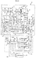
- Fig. 2 representing the circuit diagram of the embodiment shown in Fig. 1.
- Fig. 2 representing the circuit diagram of the embodiment shown in Fig. 1.
- the same components as those in Fig. 1 are designated by the same reference numerals and symbols.
- the connection, etc. between the turn-on unit 6, the control unit 7 and the laser device 9 remain same and therefore the explanation thereof is not repeated here.
- the converting circuit 10 and the laser device 9 in Fig. 2 are similar to those in Fig. 1, the description thereof is omitted, and only the turn-on circuit 6 will now be described hereinbelow.
- the turn-on circuit 6 includes the triangular wave generating circuit 1, the error amplifier 2, the PWM3, the lamp turn-on circuit 4, the xenon lamp 5 and the protection circuit 12, as described above.
- a triangular-wave voltage output having the same frequency as the frequency f1 of the triangular wave generating circuit 1 and a lamp driving voltage obtained from the lamp turn-on circuit 4 are commutated to obtain a voltage VD divided into a predetermined value.
- the voltage VD is amplified by the error amplifier 2 and applied to the PWM 3.
- the PWM 3 generates a signal subjected to pulse width modulation according to the voltage VD.
- the lamp turn-on circuit 4 has the following construction.
- An output CH of a chopper circuit 11 is connected to a central terminal TN of an input winding in a step-up transformer 25 and an anode terminal of a diode 41.
- An output of a lamp driving circuit 47 is connected to one terminal T1 of the input winding in the step-up transformer 25 and an output of a lamp driving circuit 48 is connected to the other terminal T2 of the input winding.
- a cathode terminal of the diode 41 is connected to a resistor 43 and capacitors 42 and 46.
- the resistor 43 and the capacitor 42 are connected in parallel to each other and are connected to a variable resistor 44.
- the variable resistor 44 is connected to a resistor 45.
- the resistor 45 and the capacitor 46 are grounded at the other terminal.
- a connection point between the resistor 43 and the variable resistor 44 is connected via a resistor R21 to an input terminal a of an amplifier 30 constituting the error amplifier 2.
- the resistors 43 and 45 and the variable resistor 44 constitute a voltage dividing circuit to adjust the variable resistor 44, thereby adjusting a voltage applied to the input terminal a of the amplifier 30.
- One terminal T3 of an output winding in the step-up transformer 25 is connected to one terminal of the xenon lamp 5, and the other terminal T4 of the output winding is grounded.
- the other terminal of the xenon lamp 5 is connected to a resistor 26, then grounded, and also connected to a resistor 49 as an input terminal of the protection circuit 12.
- the protection circuit 12 detects an overvoltage applied to the xenon lamp 5 and an overcurrent flowing into the xenon lamp 5, thereby preventing electric breakdown of the transformer due to the overvoltage and burning of the step-up transformer 25 due to the overcurrent.
- An anode terminal of a diode 50 is connected to the input resistor 49 of the protection circuit 12.
- One terminal of a resistor 52 and one terminal of a capacitor 51 are connected in parallel to a cathode terminal of the diode 50.
- the other terminal of the resistor 52 and the other terminal of the capacitor 51 are grounded.
- An overcurrent detecting circuit 53 and an overvoltage detecting circuit 54 which are conventionally-known, are connected in parallel to the cathode terminal of the diode 50.
- An output of the overcurrent detecting circuit 53 and an output of the overvoltage detecting circuit 54 are connected to an input of an OR circuit 55.
- An output of the OR circuit 55 is supplied to the terminal BI of the PWM 3.
- the output of the PWM 3 is connected to a clock terminal T of a toggle flip-flop 33 via an inverter circuit 32.
- Outputs Q1 and Q2 of the toggle flip-flop 33 are connected to inputs of the lamp driving circuits 47 and 48, respectively, and also connected to one input terminals I2, I2 of an AND gates 34 and 35, respectively.
- the other input terminals I1, I1 of the AND gates 34 and 35 are connected to the output of the PWM 3.
- Respective outputs of the AND gates 34 and 35 are connected to base terminals of transistors 36 and 37. Emitter terminals of the transistors 36 and 37 are grounded, and respective collector terminals thereof are connected to anode terminals of diodes 38 and 39.
- a cathode terminal of the diode 38 is connected to a cathode terminal of the diode 39.
- Cathode terminals of the diodes 38 and 39 are connected to each other, and then connected to one terminal of a resistor 56 and a driving terminal C1 of a switching circuit 24 in the chopper circuit 11.
- a plus power supply is connected to the other terminal of the resistor 56.
- the diodes 38 and 39 and the resistor 56 constitute an OR circuit.
- the chopper circuit 11 for converting a DC voltage into an AC voltage has the following configuration.
- a DC voltage C is applied to a reactor 23 via a fuse 20.
- a resistor 21 and a capacitor 22 are connected in parallel to an input of the reactor 23.
- An output terminal of the reactor 23 is connected to input terminals C and D of the switching circuit 24.
- the triangular wave generating circuit 1 generates a signal S, when receiving the clock with the frequency f1.
- a reference voltage VR is applied to the input terminal b of the amplifier 30.
- an AC output voltage is generated in the switching circuit 24 in the chopper circuit 11, rectified by the diode 41, divided by the dividing circuit constituted by the resistors 43 and 45 and the variable resistor 44, and applied to the input terminal a of the amplifier 30 as a voltage VD according to the reference voltage VR.
- the PWM 3 compares the output of the amplifier 30 with the output of the triangular wave generating circuit 1 (triangular-wave voltage) to adjust the luminance of the xenon lamp 5 at the turn-on time. Specifically, the PWM 3 increases gradually a pulse width through a conventionally-known method until the output of the amplifier 30 is obtained, and generates a PWM signal with a predetermined constant pulse width when the output of the amplifier 30 is obtained.
- Signals QT1 and QT2 are obtained such that the PWM signal is made into 1/2 by the inverter circuit 32 and the toggle flip-flop 33.
- the PMW signal and the signals QT1 and QT2 are supplied to the AND gates 34 and 35 to obtain signals G1 and G2.
- An OR signal G3 by the signals G1 and G2 is obtained by the diodes 38 and 39 and the resistor 56.
- the signal G3 is supplied to the driving terminal C1 of the switching circuit 24 in the chopper circuit 11.
- the signals QT1 and QT2 are supplied respectively to the input terminals T1 and T2 of the step-up transformer 25, and, together with the signal supplied to the driving terminal C1 of the switching circuit 24 in the chopper circuit, increased by the step-up transformer 25 up to a pulse voltage required to turn on the xenon lamp 5.
- the pulse voltage is synchronized with the signals QT1 and QT2, that is, with the reset signal R adapted to store signals in the system control unit 7, whereby no fraction is included in the pulse voltage, which is applied to the lamp between the reset signals R.
- a rare gas discharge lamp is turned on by a high AC pulse voltage and the image sensors are driven synchronously with the rare gas discharge lamp, whereby even when a lamp such as a xenon lamp is turned on at a high frequency affecting the accumulating time of each image sensor, it does not happen that the output of each image sensor fluctuates due to the fraction between the turn-on frequency and the accumulating time of each image sensor. Consequently, a stable image input device can be provided.
- the image sensor and the rare gas discharge lamp are driven synchronously with each other by controlling the turn-on circuit for the rare gas discharge lamp through an image transfer signal from each image sensor, whereby the lamp can be turned on synchronously with the timing to input the image into the system control unit.
- the lamp is not turned off during the accumulation of images and stable images can be inputted.
Landscapes
- Engineering & Computer Science (AREA)
- Multimedia (AREA)
- Signal Processing (AREA)
- Facsimile Scanning Arrangements (AREA)
- Lasers (AREA)
Applications Claiming Priority (2)
| Application Number | Priority Date | Filing Date | Title |
|---|---|---|---|
| JP2001215695A JP2003032444A (ja) | 2001-07-16 | 2001-07-16 | イメージ入力装置 |
| JP2001215695 | 2001-07-16 |
Publications (2)
| Publication Number | Publication Date |
|---|---|
| EP1280332A2 true EP1280332A2 (de) | 2003-01-29 |
| EP1280332A3 EP1280332A3 (de) | 2004-03-10 |
Family
ID=19050288
Family Applications (1)
| Application Number | Title | Priority Date | Filing Date |
|---|---|---|---|
| EP02015489A Withdrawn EP1280332A3 (de) | 2001-07-16 | 2002-07-12 | Bildeingabegerät mit Edelgas-Entladungslampe |
Country Status (3)
| Country | Link |
|---|---|
| US (1) | US6670769B2 (de) |
| EP (1) | EP1280332A3 (de) |
| JP (1) | JP2003032444A (de) |
Families Citing this family (5)
| Publication number | Priority date | Publication date | Assignee | Title |
|---|---|---|---|---|
| JP3800415B2 (ja) * | 2002-07-30 | 2006-07-26 | ミネベア株式会社 | パルス幅変調回路及びそれを用いた照明装置 |
| TW200525437A (en) * | 2004-01-28 | 2005-08-01 | Sunplus Technology Co Ltd | Device using pulse width modulation to control light source of optical mouse |
| KR100837397B1 (ko) * | 2006-01-05 | 2008-06-17 | 삼성전자주식회사 | 탄소나노튜브를 이용한 개스 센서 및 그 측정방법 |
| JP5081865B2 (ja) * | 2009-05-22 | 2012-11-28 | 京セラドキュメントソリューションズ株式会社 | 画像読取装置及び画像形成装置 |
| JP5087590B2 (ja) * | 2009-05-22 | 2012-12-05 | 京セラドキュメントソリューションズ株式会社 | 画像読取装置及び画像形成装置 |
Family Cites Families (6)
| Publication number | Priority date | Publication date | Assignee | Title |
|---|---|---|---|---|
| WO1980000647A1 (en) * | 1978-09-05 | 1980-04-03 | Thorn Electric Ind Ltd | Improvements in lamp drive circuits,and cine film projectors or cameras incorporating the same |
| JPS5953865A (ja) | 1982-09-22 | 1984-03-28 | Canon Inc | 画像読取装置 |
| US5495361A (en) * | 1995-05-08 | 1996-02-27 | Agfa Division, Bayer Corporation | Method and apparatus for synchronizing the polarization control signal of an AC-polarized arc-discharge lamp with the exposure timing signals of a CCD line sensor |
| JP2000004332A (ja) * | 1998-03-02 | 2000-01-07 | Fuji Xerox Co Ltd | 画像読取装置 |
| KR100356940B1 (ko) * | 1998-03-27 | 2002-10-18 | 황갑우 | 고압방전등용 전자식 안정기 |
| JP4018315B2 (ja) * | 2000-03-10 | 2007-12-05 | キヤノン株式会社 | 画像入力システム、光源制御方法及び記憶媒体 |
-
2001
- 2001-07-16 JP JP2001215695A patent/JP2003032444A/ja active Pending
-
2002
- 2002-07-12 EP EP02015489A patent/EP1280332A3/de not_active Withdrawn
- 2002-07-15 US US10/193,997 patent/US6670769B2/en not_active Expired - Fee Related
Non-Patent Citations (1)
| Title |
|---|
| None * |
Also Published As
| Publication number | Publication date |
|---|---|
| EP1280332A3 (de) | 2004-03-10 |
| US6670769B2 (en) | 2003-12-30 |
| JP2003032444A (ja) | 2003-01-31 |
| US20030011312A1 (en) | 2003-01-16 |
Similar Documents
| Publication | Publication Date | Title |
|---|---|---|
| US4642679A (en) | Color image reading apparatus | |
| US7173234B2 (en) | Method reading apparatus and control method thereof having an illumination unit | |
| US5296944A (en) | Image scanner and dynamic range adjusting method thereof | |
| US6386452B1 (en) | Image reading device with improved controller | |
| US5748460A (en) | Power supply apparatus | |
| US6670769B2 (en) | Image input device | |
| US20080290811A1 (en) | Power source unit for discharge lamp and method of controlling the same | |
| US5757631A (en) | Converter apparatus with reversible driving of a switching transistor | |
| US4839739A (en) | Image signal binary circuit with a variable-frequency clock signal generator for driving an image sensor | |
| EP0150847B1 (de) | Beleuchtungssteuerausstattung | |
| US5402480A (en) | Call signal generating circuit | |
| US5612857A (en) | Power supply apparatus | |
| JPS6041875A (ja) | カラ−画像読取装置 | |
| JP3881276B2 (ja) | 画像読取り装置 | |
| US4947086A (en) | System for lighting fluorescent lamps | |
| US6735000B2 (en) | Image reading apparatus and method | |
| US5010394A (en) | Automatic white balance circuit capable of effectively adjusting white balance under a flashing light source | |
| EP0499636B1 (de) | Sequentieller farbabtaster mit synchronisiertem variablen verschluss | |
| JP3625382B2 (ja) | 画像読取り装置 | |
| KR100248226B1 (ko) | 화상독취기의 밝기조정방법 및 그 장치 | |
| US7091674B2 (en) | Rare gas fluorescent lamp device | |
| CN119225098A (zh) | 激光投影设备及其控制方法 | |
| WO2025031050A1 (zh) | 光源系统及激光投影设备 | |
| CN119225100A (zh) | 激光投影设备及其控制方法 | |
| JP3474999B2 (ja) | ビデオカメラ |
Legal Events
| Date | Code | Title | Description |
|---|---|---|---|
| PUAI | Public reference made under article 153(3) epc to a published international application that has entered the european phase |
Free format text: ORIGINAL CODE: 0009012 |
|
| AK | Designated contracting states |
Designated state(s): AT BE BG CH CY CZ DE DK EE ES FI FR GB GR IE IT LI LU MC NL PT SE SK TR |
|
| AX | Request for extension of the european patent |
Extension state: AL LT LV MK RO SI |
|
| PUAL | Search report despatched |
Free format text: ORIGINAL CODE: 0009013 |
|
| AK | Designated contracting states |
Kind code of ref document: A3 Designated state(s): AT BE BG CH CY CZ DE DK EE ES FI FR GB GR IE IT LI LU MC NL PT SE SK TR |
|
| AX | Request for extension of the european patent |
Extension state: AL LT LV MK RO SI |
|
| 17P | Request for examination filed |
Effective date: 20040823 |
|
| AKX | Designation fees paid |
Designated state(s): DE FR GB IT NL |
|
| 17Q | First examination report despatched |
Effective date: 20070320 |
|
| STAA | Information on the status of an ep patent application or granted ep patent |
Free format text: STATUS: THE APPLICATION IS DEEMED TO BE WITHDRAWN |
|
| 18D | Application deemed to be withdrawn |
Effective date: 20100202 |