EP1281439A1 - Vorrichtung zur Aufnahme eines chipförmigen Trägers und Verfahren zum Zusammenbau mehrerer solcher Vorrichtungen - Google Patents
Vorrichtung zur Aufnahme eines chipförmigen Trägers und Verfahren zum Zusammenbau mehrerer solcher Vorrichtungen Download PDFInfo
- Publication number
- EP1281439A1 EP1281439A1 EP01118247A EP01118247A EP1281439A1 EP 1281439 A1 EP1281439 A1 EP 1281439A1 EP 01118247 A EP01118247 A EP 01118247A EP 01118247 A EP01118247 A EP 01118247A EP 1281439 A1 EP1281439 A1 EP 1281439A1
- Authority
- EP
- European Patent Office
- Prior art keywords
- chip
- cavity
- shaped carrier
- sealing material
- chip shaped
- Prior art date
- Legal status (The legal status is an assumption and is not a legal conclusion. Google has not performed a legal analysis and makes no representation as to the accuracy of the status listed.)
- Withdrawn
Links
Images


Classifications
-
- H—ELECTRICITY
- H10—SEMICONDUCTOR DEVICES; ELECTRIC SOLID-STATE DEVICES NOT OTHERWISE PROVIDED FOR
- H10P—GENERIC PROCESSES OR APPARATUS FOR THE MANUFACTURE OR TREATMENT OF DEVICES COVERED BY CLASS H10
- H10P72/00—Handling or holding of wafers, substrates or devices during manufacture or treatment thereof
- H10P72/04—Apparatus for manufacture or treatment
- H10P72/0446—Apparatus for mounting on conductive members, e.g. leadframes or conductors on insulating substrates
-
- B—PERFORMING OPERATIONS; TRANSPORTING
- B01—PHYSICAL OR CHEMICAL PROCESSES OR APPARATUS IN GENERAL
- B01L—CHEMICAL OR PHYSICAL LABORATORY APPARATUS FOR GENERAL USE
- B01L3/00—Containers or dishes for laboratory use, e.g. laboratory glassware; Droppers
- B01L3/50—Containers for the purpose of retaining a material to be analysed, e.g. test tubes
- B01L3/508—Rigid containers without fluid transport within
-
- B—PERFORMING OPERATIONS; TRANSPORTING
- B01—PHYSICAL OR CHEMICAL PROCESSES OR APPARATUS IN GENERAL
- B01L—CHEMICAL OR PHYSICAL LABORATORY APPARATUS FOR GENERAL USE
- B01L9/00—Supporting devices; Holding devices
- B01L9/52—Supports specially adapted for flat sample carriers, e.g. for plates, slides, chips
- B01L9/527—Supports specially adapted for flat sample carriers, e.g. for plates, slides, chips for microfluidic devices, e.g. used for lab-on-a-chip
-
- H—ELECTRICITY
- H10—SEMICONDUCTOR DEVICES; ELECTRIC SOLID-STATE DEVICES NOT OTHERWISE PROVIDED FOR
- H10P—GENERIC PROCESSES OR APPARATUS FOR THE MANUFACTURE OR TREATMENT OF DEVICES COVERED BY CLASS H10
- H10P72/00—Handling or holding of wafers, substrates or devices during manufacture or treatment thereof
- H10P72/04—Apparatus for manufacture or treatment
- H10P72/0438—Apparatus for making assemblies not otherwise provided for, e.g. package constructions
-
- B—PERFORMING OPERATIONS; TRANSPORTING
- B01—PHYSICAL OR CHEMICAL PROCESSES OR APPARATUS IN GENERAL
- B01J—CHEMICAL OR PHYSICAL PROCESSES, e.g. CATALYSIS OR COLLOID CHEMISTRY; THEIR RELEVANT APPARATUS
- B01J2219/00—Chemical, physical or physico-chemical processes in general; Their relevant apparatus
- B01J2219/00274—Sequential or parallel reactions; Apparatus and devices for combinatorial chemistry or for making arrays; Chemical library technology
-
- B—PERFORMING OPERATIONS; TRANSPORTING
- B01—PHYSICAL OR CHEMICAL PROCESSES OR APPARATUS IN GENERAL
- B01J—CHEMICAL OR PHYSICAL PROCESSES, e.g. CATALYSIS OR COLLOID CHEMISTRY; THEIR RELEVANT APPARATUS
- B01J2219/00—Chemical, physical or physico-chemical processes in general; Their relevant apparatus
- B01J2219/00274—Sequential or parallel reactions; Apparatus and devices for combinatorial chemistry or for making arrays; Chemical library technology
- B01J2219/00277—Apparatus
- B01J2219/00497—Features relating to the solid phase supports
- B01J2219/00527—Sheets
- B01J2219/00529—DNA chips
-
- B—PERFORMING OPERATIONS; TRANSPORTING
- B01—PHYSICAL OR CHEMICAL PROCESSES OR APPARATUS IN GENERAL
- B01J—CHEMICAL OR PHYSICAL PROCESSES, e.g. CATALYSIS OR COLLOID CHEMISTRY; THEIR RELEVANT APPARATUS
- B01J2219/00—Chemical, physical or physico-chemical processes in general; Their relevant apparatus
- B01J2219/00274—Sequential or parallel reactions; Apparatus and devices for combinatorial chemistry or for making arrays; Chemical library technology
- B01J2219/00583—Features relative to the processes being carried out
- B01J2219/00596—Solid-phase processes
-
- B—PERFORMING OPERATIONS; TRANSPORTING
- B01—PHYSICAL OR CHEMICAL PROCESSES OR APPARATUS IN GENERAL
- B01J—CHEMICAL OR PHYSICAL PROCESSES, e.g. CATALYSIS OR COLLOID CHEMISTRY; THEIR RELEVANT APPARATUS
- B01J2219/00—Chemical, physical or physico-chemical processes in general; Their relevant apparatus
- B01J2219/00274—Sequential or parallel reactions; Apparatus and devices for combinatorial chemistry or for making arrays; Chemical library technology
- B01J2219/00583—Features relative to the processes being carried out
- B01J2219/00603—Making arrays on substantially continuous surfaces
- B01J2219/00605—Making arrays on substantially continuous surfaces the compounds being directly bound or immobilised to solid supports
- B01J2219/00608—DNA chips
-
- B—PERFORMING OPERATIONS; TRANSPORTING
- B01—PHYSICAL OR CHEMICAL PROCESSES OR APPARATUS IN GENERAL
- B01J—CHEMICAL OR PHYSICAL PROCESSES, e.g. CATALYSIS OR COLLOID CHEMISTRY; THEIR RELEVANT APPARATUS
- B01J2219/00—Chemical, physical or physico-chemical processes in general; Their relevant apparatus
- B01J2219/00274—Sequential or parallel reactions; Apparatus and devices for combinatorial chemistry or for making arrays; Chemical library technology
- B01J2219/00583—Features relative to the processes being carried out
- B01J2219/00603—Making arrays on substantially continuous surfaces
- B01J2219/00605—Making arrays on substantially continuous surfaces the compounds being directly bound or immobilised to solid supports
- B01J2219/00612—Making arrays on substantially continuous surfaces the compounds being directly bound or immobilised to solid supports the surface being inorganic
-
- B—PERFORMING OPERATIONS; TRANSPORTING
- B01—PHYSICAL OR CHEMICAL PROCESSES OR APPARATUS IN GENERAL
- B01J—CHEMICAL OR PHYSICAL PROCESSES, e.g. CATALYSIS OR COLLOID CHEMISTRY; THEIR RELEVANT APPARATUS
- B01J2219/00—Chemical, physical or physico-chemical processes in general; Their relevant apparatus
- B01J2219/00274—Sequential or parallel reactions; Apparatus and devices for combinatorial chemistry or for making arrays; Chemical library technology
- B01J2219/00583—Features relative to the processes being carried out
- B01J2219/00603—Making arrays on substantially continuous surfaces
- B01J2219/00605—Making arrays on substantially continuous surfaces the compounds being directly bound or immobilised to solid supports
- B01J2219/00632—Introduction of reactive groups to the surface
- B01J2219/00637—Introduction of reactive groups to the surface by coating it with another layer
-
- B—PERFORMING OPERATIONS; TRANSPORTING
- B01—PHYSICAL OR CHEMICAL PROCESSES OR APPARATUS IN GENERAL
- B01J—CHEMICAL OR PHYSICAL PROCESSES, e.g. CATALYSIS OR COLLOID CHEMISTRY; THEIR RELEVANT APPARATUS
- B01J2219/00—Chemical, physical or physico-chemical processes in general; Their relevant apparatus
- B01J2219/00274—Sequential or parallel reactions; Apparatus and devices for combinatorial chemistry or for making arrays; Chemical library technology
- B01J2219/00583—Features relative to the processes being carried out
- B01J2219/00603—Making arrays on substantially continuous surfaces
- B01J2219/00659—Two-dimensional arrays
-
- B—PERFORMING OPERATIONS; TRANSPORTING
- B01—PHYSICAL OR CHEMICAL PROCESSES OR APPARATUS IN GENERAL
- B01J—CHEMICAL OR PHYSICAL PROCESSES, e.g. CATALYSIS OR COLLOID CHEMISTRY; THEIR RELEVANT APPARATUS
- B01J2219/00—Chemical, physical or physico-chemical processes in general; Their relevant apparatus
- B01J2219/00274—Sequential or parallel reactions; Apparatus and devices for combinatorial chemistry or for making arrays; Chemical library technology
- B01J2219/0068—Means for controlling the apparatus of the process
- B01J2219/00702—Processes involving means for analysing and characterising the products
- B01J2219/00707—Processes involving means for analysing and characterising the products separated from the reactor apparatus
-
- B—PERFORMING OPERATIONS; TRANSPORTING
- B01—PHYSICAL OR CHEMICAL PROCESSES OR APPARATUS IN GENERAL
- B01J—CHEMICAL OR PHYSICAL PROCESSES, e.g. CATALYSIS OR COLLOID CHEMISTRY; THEIR RELEVANT APPARATUS
- B01J2219/00—Chemical, physical or physico-chemical processes in general; Their relevant apparatus
- B01J2219/00274—Sequential or parallel reactions; Apparatus and devices for combinatorial chemistry or for making arrays; Chemical library technology
- B01J2219/00718—Type of compounds synthesised
- B01J2219/0072—Organic compounds
- B01J2219/00722—Nucleotides
-
- B—PERFORMING OPERATIONS; TRANSPORTING
- B01—PHYSICAL OR CHEMICAL PROCESSES OR APPARATUS IN GENERAL
- B01L—CHEMICAL OR PHYSICAL LABORATORY APPARATUS FOR GENERAL USE
- B01L2200/00—Solutions for specific problems relating to chemical or physical laboratory apparatus
- B01L2200/06—Fluid handling related problems
- B01L2200/0689—Sealing
-
- B—PERFORMING OPERATIONS; TRANSPORTING
- B01—PHYSICAL OR CHEMICAL PROCESSES OR APPARATUS IN GENERAL
- B01L—CHEMICAL OR PHYSICAL LABORATORY APPARATUS FOR GENERAL USE
- B01L2300/00—Additional constructional details
- B01L2300/06—Auxiliary integrated devices, integrated components
- B01L2300/0627—Sensor or part of a sensor is integrated
- B01L2300/0636—Integrated biosensor, microarrays
-
- B—PERFORMING OPERATIONS; TRANSPORTING
- B01—PHYSICAL OR CHEMICAL PROCESSES OR APPARATUS IN GENERAL
- B01L—CHEMICAL OR PHYSICAL LABORATORY APPARATUS FOR GENERAL USE
- B01L2300/00—Additional constructional details
- B01L2300/08—Geometry, shape and general structure
- B01L2300/0809—Geometry, shape and general structure rectangular shaped
-
- B—PERFORMING OPERATIONS; TRANSPORTING
- B01—PHYSICAL OR CHEMICAL PROCESSES OR APPARATUS IN GENERAL
- B01L—CHEMICAL OR PHYSICAL LABORATORY APPARATUS FOR GENERAL USE
- B01L2400/00—Moving or stopping fluids
- B01L2400/06—Valves, specific forms thereof
- B01L2400/0677—Valves, specific forms thereof phase change valves; Meltable, freezing, dissolvable plugs; Destructible barriers
-
- B—PERFORMING OPERATIONS; TRANSPORTING
- B01—PHYSICAL OR CHEMICAL PROCESSES OR APPARATUS IN GENERAL
- B01L—CHEMICAL OR PHYSICAL LABORATORY APPARATUS FOR GENERAL USE
- B01L9/00—Supporting devices; Holding devices
- B01L9/52—Supports specially adapted for flat sample carriers, e.g. for plates, slides, chips
-
- C—CHEMISTRY; METALLURGY
- C40—COMBINATORIAL TECHNOLOGY
- C40B—COMBINATORIAL CHEMISTRY; LIBRARIES, e.g. CHEMICAL LIBRARIES
- C40B40/00—Libraries per se, e.g. arrays, mixtures
- C40B40/04—Libraries containing only organic compounds
- C40B40/06—Libraries containing nucleotides or polynucleotides, or derivatives thereof
-
- Y—GENERAL TAGGING OF NEW TECHNOLOGICAL DEVELOPMENTS; GENERAL TAGGING OF CROSS-SECTIONAL TECHNOLOGIES SPANNING OVER SEVERAL SECTIONS OF THE IPC; TECHNICAL SUBJECTS COVERED BY FORMER USPC CROSS-REFERENCE ART COLLECTIONS [XRACs] AND DIGESTS
- Y10—TECHNICAL SUBJECTS COVERED BY FORMER USPC
- Y10S—TECHNICAL SUBJECTS COVERED BY FORMER USPC CROSS-REFERENCE ART COLLECTIONS [XRACs] AND DIGESTS
- Y10S435/00—Chemistry: molecular biology and microbiology
- Y10S435/809—Incubators or racks or holders for culture plates or containers
Definitions
- the present invention relates to a device for receiving a chip shaped carrier having an active surface which is adapted to be read by an electro-optical reading device.
- the invention further relates to a process for assembling a plurality of such chip receiving devices.
- the invention further relates to a system for carrying out evaluation and/or monitoring methods involving electro-optical reading of an active surface of a chip shaped carrier.
- a chip shaped carrier is a substrate, in particular a glass chip of e.g. squared shape having a thickness of e.g. 0.7 or 1.0 millimeter and a so called active surface, which is a surface coated with an array of different snippets of DNA, e.g. DNA oligonucleotide probes, located at known positions on that surface. Those snippets of DNA serve as probes for detecting DNA fragments with a complementary DNA sequence.
- a receiving device for receiving such a DNA chip is in particular a one-way cartridge made of a plastic material, and a cartridge hosting a DNA chip is called an analytical cartridge.
- DNA chips contained in such cartridges have a wide range of applications. For example, they may be used for understanding the structure-activity relationship between different biological materials or determining the DNA-sequence of an unknown biological material. For instance, the DNA-sequence of such unknown material may be determined by, for example, a process known as sequencing by hybridization.
- sequencing by hybridization a sequences of diverse materials are formed at known locations on a surface of a chip, and a solution containing one or more targets to be sequenced is applied to that surface. The targets will bind or hybridize with only complementary sequences on the substrate.
- the locations at which hybridization occurs are detected with appropriate detection systems by labeling the targets with a fluorescent dye, radioactive isotope, enzyme, or other marker. Information about target sequences can be extracted from the data obtained by such detection systems.
- the active coating of the chip that is the surface thereof which is coated with the above mentioned diverse sequences, has to be accessible e.g. to optical detection means, e.g. in the case of fluorescence measurements, the chip has to be inserted into the outer wall of a one-way cartridge, and its active coating faces the interior of the so-called process chamber within the cartridge.
- processing of the active coating of the chip includes flooding of the process chamber of the cartridge with a solution containing one or more targets to be sequenced. Therefore, a liquid-tight connection between the chip and the one-way cartridge is necessary.
- this has been achieved under clean-room conditions by attaching the chip to a cavity of the cartridge by means of an adhesive, that is by gluing it into the cartridge.
- This known method for connecting the chip to the cartridge has serious disadvantages.
- the fluorescence of the adhesives used is so high that it substantially interferes and perturbates fluorescence measurements performed on the active coating of the chips and can even have saturating effect on a photomultiplier used for performing the fluorescence measurements.
- the adhesive has to be applied by a dispenser, which is not possible with any adhesive.
- the known adhesives are prone to develop or contain gases, which when freed would disturb the reactions.
- Another problem is occasioned by solvent present in the adhesive because the solvent may react with the DNA samples on the active surface. It has even be found that solvent negatively influence the properties of the glass surface of a chip shaped carrier, e.g. blurs it.
- a further disadvantage of the known method for connecting the chip to the cartridge is that it is performed manually and is not suitable for being performed by automated means, because a very careful positioning within the receiving window of the cartridge is necessary. Furthermore, as the adhesive is applied thereafter, a second control, if the DNA chip is still in place, has to be performed. These operations are aggravated by the relatively large tolerances of the dimensions of the chips and their rather uneven edges.
- a first aim of the invention is therefore to provide a device for receiving a chip of the above mentioned kind which avoids at least one of the above-given disadvantages, and preferably all of it.
- a second aim of the invention is to provide a process for assembling a plurality of chip receiving devices according to the invention with a high throughput.
- a third aim of the invention is to provide a system for carrying out evaluation and/or monitoring methods involving electro-optical reading of an active surface of a chip shaped carrier with avoiding at least one of the above mentioned disadvantages of prior art embodiments.
- a fourth aim of the present invention consist in proposing a method for more conveniently placing a first object in a second object and to fasten it there.
- a device, by which the first aim is attained, is defined in claim 1.
- the subsequent claims propose preferred embodiments.
- the main advantages of a chip receiving device are due to the fact that the required liquid-tight connection of the chip to the cartridge is achieved in providing a sealing material which can be fluidized.
- the sealing material constitutes a substantial part of the wall of the socket for a chip in the cartridge, thereby defining more exactly the position of the chip when it is set in the socket.
- the sealing material closes the space between the solid walls of the socket and the chip. Due to its liquid state, any irregularity of the edges of the chip do not impair the sealing.
- the chip remains fluid-tight even if a sensible overpressure is applied, e.g. exerted by a liquid filled in the chamber of the cartridge.
- sealing material a material which can be molten in applying heat and resolidifies in cooling down.
- a hotmelt material particularly a hotmelt adhesive, i.e. an adhesive fusible by heat, also known as "thermoplastic adhesive”.
- the above mentioned second aim is attained with a process for assembling a plurality of chip receiving devices according to the invention, according to claim 11.
- the claims depending thereon define preferred manners of execution.
- the above mentioned third aim is attained with a system for carrying out evaluation and/or monitoring methods involving electro-optical reading of an active surface of a chip shaped carrier, according to claim 15.
- the further dependent claims define preferred embodiments thereof.
- the main advantage of a system according to the invention is that it makes possible to carry out evaluation and/or monitoring methods involving electro-optical readings of an active surface of a chip shaped carrier of the above mentioned type with suppressing the above mentioned drawbacks of prior art equipment.
- the fourth aim is specifically attained by the method according to claim 17.
- the rim of the seat is constituted at least to a sufficient part by a hot melt material.
- the hot melt is solid under normal conditions, it can be quite exactly adapted to the geometry of the second object(s), and the latter when placed into the seat, are exactly registered therein. Thereby, an additional control of exact position of the second object may be waived.
- the hotmelt is locally heated in order to render it liquid and to fasten the second object(s) in their seat.
- the first object including the parts made of hot melt may be manufactured long time before the second objects are added and fastened.
- the hot melt or more generally, the material which is liquidifiable and resolidifies again afterwards, constitutes a solid, integral part of the first object and may be reactivated, e.g. by irradiation using laser light, to behave as a glue and/or a fluid sealing material.
- a chip receiving device comprises a cartridge 12.
- Cartridge 12 comprises a first casing part 14 and a second casing part 15.
- Casing part 15 has an opening 13 for introducing a liquid sample into cartridge 12.
- Casing part 15 is preferably made of an optically non-transparent material.
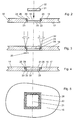
- casing part 14 has an outer surface 16 and inner surface 17, a first cavity 18 for receiving a chip shaped carrier 21 - called for simplicity chip 21 hereinafter- and a second cavity 22 which forms a window providing access to said first cavity 18 and thereby to the active surface of chip shaped carrier 21.
- the just described structure is just one example of means which provide visual access to that active surface.
- chip 21 is made of glass, has a thickness of 0.7 or 1.0 millimeter, and has substantially the shape of a square. Since the size of chip 21 has a relatively high dimensional tolerance of e.g. 0.0762 millimeter of length and width, in the embodiment described hereinafter the space available in cavity 18 for receiving and positioning chip 21 has a corresponding joint clearance 20 (cf. Fig. 6).
- Chip 21 has an active surface 28 which is covered by oligonucleotide probes 32 and which must not be touched at all to avoid any damage of the probes 32.
- Cavity 18 has a flat bottom surface 23 and side wall surfaces 24 which extend between outer surface 16 of casing 14 and bottom surface 23.
- the side walls 24 are provided with a layer of a sealing hotmelt material 26.
- the hotmelt is fusible by heating, specifically by insolating laser light, and solidifies again when cooling down.
- the hotmelt material is one of the adhesive.
- the inner surfaces 29 of the hotmelt material 26 may be inclined so that an opening tapering to the bottom surface 23 is obtained. For this purpose, the tapering caused by injection moulding of this piece may suffice.
- the bottom surface 23 has an opening 25 which opens into second cavity 22.
- chip 21 is positioned in cavity 18 of casing part 14.
- the hotmelt 26 is heated by insolating laser light 30 from a suitable light source.
- the laser light is directed sequentially or simultaneously to the whole hotmelt material 26.
- the heated hotmelt gets fluid and fills the clearance 20 between walls 24 and the edge of the chip 21.
- irregularities in the shape of the edge 31 of the chip 21 do not have any sensible influence on this process, neither on the quality of the bond between the hotmelt 26 and the chip 21.
- Figs. 4 and 5 show the fixed state in a cross-sectional and a top view, respectively. Particularly in Fig. 4, it is evident that the hotmelt 26 has filled up the clearance 20 from the bottom.
- chip 21 has a first surface 61 which is coated with a so called probe array 32, i.e. an array of diverse sequences, e.g. DNA oligonucleotides, located at known positions on that first surface, and a second surface 62 opposite to said first surface.
- a third surface 63 which extends between said first and second surfaces, is normal to these surfaces, and is the outer surface of the lateral periphery of chip 21.
- chip 21 Since the probe array 32 of chip 21 has to be accessible e.g. to optical detection means, e.g. for performing fluorescence measurements, chip 21 is inserted into the outer wall of cartridge 12, and its first surface 61 with the probe array 32 faces the interior of a so-called process chamber 33 within cartridge 12.
- a chip 21 may usually have three sizes designated by numbers 100, 169 and 400 and is substantially quadratic in shape.
- Chip size 100 has a side length 70 of 10.92 millimeters.
- Chip size 169 has a side length 70 of 8.153 millimeters.
- Chip size 400 has a side length 70 of 5.384 millimeters.
- the active surface of chip size 100 has a side length 71 of 9.5 millimeters.
- the active surface of chip 21 size 169 has a side length 71 of 6.73 millimeters.
- the active surface of chip size 400 has a side length 71 of 3.96 millimeters. Thickness 73 of the chip 21 is about 0,7 mm.
- a further aspect of the invention relates to a process for an automated assembly of a plurality of chip receiving devices according to the invention.
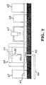
- Fig. 7 schematically shows the structure of an completely automatic assembly line for carrying out such a process.
- This assembly line comprises a stock 41 of casing parts 14, 15 of cartridges 12, a first conveyor 42, a die bonder 43, a second conveyor 44 for conveying blue tapes which come from a diamond saw cutting machine and which carry a plurality of chip shaped carriers 21, a laser welding machine 47, an automatic packaging apparatus 48, and a stock of completely assembled chip receiving devices 49.
- Assembly line components 42 to 48 are all standard apparatuses and devices suitable for automated operation.
- Die bonder 43 comprises a blue tape support 45 having an expansion mechanism, a working frame 52 movable in x- and y-direction and a tool holder 53 which holds a die collet 46.
- Tool holder 53 is connected to working frame 52 and is thereby movable in x-and y-direction.
- Tool holder 53 has a means, e.g. a spindle, which enables to move die collet 46 in z-direction.
- a process for assembling a plurality of analytical cartridges comprising cartridges 12 comprises the following steps:
- casings 14 are preferably transferred one-by-one via first conveyor 42 from the stock of parts 41 to die bonder 43 and from there successively to the other parts of the assembly line where a processing step has to be carried out.
- chip shaped carriers 21 are also transferred one-by-one via second conveyor 44 and blue tape support 45 to the die bonder 43.
- the active surface 28 of chip 21 and particularly the probes 32 thereon are not touched at all, and this ensures that no damage of that active surface can take place during the assembling process.
- the above defined process ensures that the quality of the cutting of chip 21 remains basically unchanged.
- this casing part and a complementary casing part 15 are forwarded to an automatic packaging apparatus 48, where they are put together to form a complete chip receiving device, that is a cartridge 12 containing a chip shaped carrier 21.
- An outstanding advantage of the device and the assembling process according to the invention is that they allow adjustment of the lateral insertion clearance when inserting the chip in cavity 18 of casing part 14. This adjustment possibility eliminates on the one hand the need for a highly accurate positioning of chip 21 in its mounting and the need for relatively large forces for effecting that mounting, and on the other hand allows the use of commercially available standard appliances for the automated manufacture of integrated circuits.
- An example of such a standard appliance is e.g. a die bonder which can supply a maximum joining force of 10 Newton.
- a die bonder is typically used for bonding an electronic silicon chip on a so-called lead frame.
- a system for carrying out evaluation and/or monitoring methods involving electro-optical reading of an active surface of a chip shaped carrier comprises
- Electro-optical reading means 51 can be e.g. a fluorometer, that is an apparatus comprising a light source for irradiating active surface 28 with an excitation beam, light detection means for detecting fluorescent light emitted by the probe array 32 on the active surface 28 and providing a corresponding output signal and means for evaluating and/or monitoring that output signal.
- a fluorometer that is an apparatus comprising a light source for irradiating active surface 28 with an excitation beam, light detection means for detecting fluorescent light emitted by the probe array 32 on the active surface 28 and providing a corresponding output signal and means for evaluating and/or monitoring that output signal.
Landscapes
- Chemical & Material Sciences (AREA)
- Health & Medical Sciences (AREA)
- Chemical Kinetics & Catalysis (AREA)
- Analytical Chemistry (AREA)
- Clinical Laboratory Science (AREA)
- General Health & Medical Sciences (AREA)
- Dispersion Chemistry (AREA)
- Hematology (AREA)
- Apparatus Associated With Microorganisms And Enzymes (AREA)
- Measuring Or Testing Involving Enzymes Or Micro-Organisms (AREA)
- Pressure Welding/Diffusion-Bonding (AREA)
- Investigating, Analyzing Materials By Fluorescence Or Luminescence (AREA)
- Container, Conveyance, Adherence, Positioning, Of Wafer (AREA)
- Optical Measuring Cells (AREA)
Priority Applications (10)
| Application Number | Priority Date | Filing Date | Title |
|---|---|---|---|
| EP01118247A EP1281439A1 (de) | 2001-07-30 | 2001-07-30 | Vorrichtung zur Aufnahme eines chipförmigen Trägers und Verfahren zum Zusammenbau mehrerer solcher Vorrichtungen |
| CA2391045A CA2391045C (en) | 2001-07-30 | 2002-06-20 | Device for receiving a chip shaped carrier and process for assembling a plurality of such devices |
| EP08003958A EP1955769B1 (de) | 2001-07-30 | 2002-07-09 | Verfahren zur Positionierung und Befestigung eines Objekts in einem anderen Objekt |
| DE60225976T DE60225976T2 (de) | 2001-07-30 | 2002-07-09 | Vorrichtung zur Aufnahme eines chipförmigen Trägers und Verfahren zum Zusammenbau mehrerer solcher Vorrichtungen |
| AT02077768T ATE391555T1 (de) | 2001-07-30 | 2002-07-09 | Vorrichtung zur aufnahme eines chipförmigen trägers und verfahren zum zusammenbau mehrerer solcher vorrichtungen |
| EP02077768A EP1281440B1 (de) | 2001-07-30 | 2002-07-09 | Vorrichtung zur Aufnahme eines chipförmigen Trägers und Verfahren zum Zusammenbau mehrerer solcher Vorrichtungen |
| AT08003958T ATE523253T1 (de) | 2001-07-30 | 2002-07-09 | Verfahren zur positionierung und befestigung eines objekts in einem anderen objekt |
| US10/205,734 US6756224B2 (en) | 2001-07-30 | 2002-07-26 | Device for receiving a chip shaped carrier and process for assembling a plurality of such devices |
| JP2002219013A JP2003130876A (ja) | 2001-07-30 | 2002-07-29 | チップ状キャリヤを受け取るためのデバイス及び複数の同デバイスを組み立てるための方法 |
| US10/870,350 US20040229383A1 (en) | 2001-07-30 | 2004-06-16 | Device for receiving a chip shaped carrier and process for assembling a plurality of such devices |
Applications Claiming Priority (1)
| Application Number | Priority Date | Filing Date | Title |
|---|---|---|---|
| EP01118247A EP1281439A1 (de) | 2001-07-30 | 2001-07-30 | Vorrichtung zur Aufnahme eines chipförmigen Trägers und Verfahren zum Zusammenbau mehrerer solcher Vorrichtungen |
Publications (1)
| Publication Number | Publication Date |
|---|---|
| EP1281439A1 true EP1281439A1 (de) | 2003-02-05 |
Family
ID=8178166
Family Applications (3)
| Application Number | Title | Priority Date | Filing Date |
|---|---|---|---|
| EP01118247A Withdrawn EP1281439A1 (de) | 2001-07-30 | 2001-07-30 | Vorrichtung zur Aufnahme eines chipförmigen Trägers und Verfahren zum Zusammenbau mehrerer solcher Vorrichtungen |
| EP02077768A Expired - Lifetime EP1281440B1 (de) | 2001-07-30 | 2002-07-09 | Vorrichtung zur Aufnahme eines chipförmigen Trägers und Verfahren zum Zusammenbau mehrerer solcher Vorrichtungen |
| EP08003958A Expired - Lifetime EP1955769B1 (de) | 2001-07-30 | 2002-07-09 | Verfahren zur Positionierung und Befestigung eines Objekts in einem anderen Objekt |
Family Applications After (2)
| Application Number | Title | Priority Date | Filing Date |
|---|---|---|---|
| EP02077768A Expired - Lifetime EP1281440B1 (de) | 2001-07-30 | 2002-07-09 | Vorrichtung zur Aufnahme eines chipförmigen Trägers und Verfahren zum Zusammenbau mehrerer solcher Vorrichtungen |
| EP08003958A Expired - Lifetime EP1955769B1 (de) | 2001-07-30 | 2002-07-09 | Verfahren zur Positionierung und Befestigung eines Objekts in einem anderen Objekt |
Country Status (6)
| Country | Link |
|---|---|
| US (2) | US6756224B2 (de) |
| EP (3) | EP1281439A1 (de) |
| JP (1) | JP2003130876A (de) |
| AT (2) | ATE391555T1 (de) |
| CA (1) | CA2391045C (de) |
| DE (1) | DE60225976T2 (de) |
Cited By (5)
| Publication number | Priority date | Publication date | Assignee | Title |
|---|---|---|---|---|
| DE10318219A1 (de) * | 2003-04-22 | 2004-11-11 | Febit Ag | Handhabungs- und Schutzgehäuse für einen Biochip, insbesondere für einen mikrofluidischen Reaktionsträger |
| DE10316723A1 (de) * | 2003-04-09 | 2004-11-18 | Siemens Ag | Probenplatte zum Einbau in eine Gehäusestruktur |
| DE10336849A1 (de) * | 2003-08-11 | 2005-03-10 | Thinxxs Gmbh | Flusszelle |
| EP3127148A4 (de) * | 2014-03-31 | 2017-11-15 | Multerra Bio, Inc. | Kostengünstige verpackung für eine flüssigkeits- und vorrichtungs-cointegration |
| CN109794308A (zh) * | 2017-11-17 | 2019-05-24 | 长光华大基因测序设备(长春)有限公司 | 一种生物芯片承载架 |
Families Citing this family (20)
| Publication number | Priority date | Publication date | Assignee | Title |
|---|---|---|---|---|
| GB2377402B (en) * | 2001-07-12 | 2004-05-12 | Agilent Technologies Inc | Improved diebond strip |
| ES2298424T3 (es) * | 2001-09-20 | 2008-05-16 | Ricoh Company, Ltd. | Procedimiento de impresion con chorro de tinta, dispositivo de impresion, juego de tinta/medio de impresion, material de impresion. |
| DE10201463B4 (de) * | 2002-01-16 | 2005-07-21 | Clondiag Chip Technologies Gmbh | Reaktionsgefäß zur Durchführung von Array-Verfahren |
| DE10323197B4 (de) * | 2003-05-22 | 2008-10-02 | Clondiag Chip Technologies Gmbh | Vorrichtung zur Halterung und Detektion von Substanzbibliotheken |
| DE10336375A1 (de) * | 2003-08-06 | 2004-12-02 | Infineon Technologies Ag | Verfahren zum Bestücken von Probenhaltern mit Biochips und Vorrichtungen zur Durchführung des Verfahrens |
| DE602004009775T2 (de) | 2004-07-02 | 2008-08-28 | Roche Diagnostics Gmbh | Vorrichtung zur zuverlässige Analyse |
| FR2889591B1 (fr) * | 2005-08-02 | 2008-04-25 | Biolumine Sa | Biocapteur en phase immobilisee |
| KR101414232B1 (ko) * | 2007-08-02 | 2014-08-06 | 삼성전자 주식회사 | 바이오 칩 패키지 및 바이오 칩 패키지 기판 |
| JP5274798B2 (ja) * | 2007-08-20 | 2013-08-28 | 東洋ゴム工業株式会社 | 研磨パッド及びその製造方法 |
| US20090286692A1 (en) * | 2008-04-15 | 2009-11-19 | Wainwright Norman R | Cartridge and Method for Sample Analysis |
| FR3084204B1 (fr) * | 2018-07-18 | 2021-05-14 | Commissariat Energie Atomique | Procede d'integration de structures dans un support et dispositif associe |
| TWI671399B (zh) * | 2018-10-22 | 2019-09-11 | 國立清華大學 | 細胞培養裝置及細胞培養系統 |
| KR20220092857A (ko) * | 2019-08-29 | 2022-07-04 | 아스트라베우스 | 마이크로유체 디바이스를 클램핑하기 위한 장치 및 방법 |
| CN214606597U (zh) * | 2020-04-24 | 2021-11-05 | 珠海艾派克微电子有限公司 | 一种耗材容器的包装件以及耗材容器 |
| CN112156819B (zh) * | 2020-08-25 | 2022-05-10 | 华东师范大学重庆研究院 | 一种大幅面阵列飞秒激光微流控芯片直印方法及其设备 |
| CN113604345B (zh) * | 2021-08-12 | 2024-04-12 | 东南大学 | 基于磁镊系统中纳米孔检测芯片的便携式装夹装置 |
| CN113953271B (zh) * | 2021-09-01 | 2022-08-19 | 国家能源集团宝庆发电有限公司 | 一种激光清洗和无损检测系统及方法 |
| CN115360128B (zh) * | 2022-10-24 | 2023-01-24 | 高能瑞泰(山东)电子科技有限公司 | 一种可辅助安装的芯片封装装置 |
| CN117334644B (zh) * | 2023-11-29 | 2024-02-13 | 四川弘智远大科技有限公司 | 一种集成电路封装的实时固化结构 |
| CN119500296B (zh) * | 2024-11-04 | 2025-10-03 | 浙江大学 | 一种集成偶联活性膜的数字微流控芯片及其制备方法和应用 |
Citations (8)
| Publication number | Priority date | Publication date | Assignee | Title |
|---|---|---|---|---|
| US3654688A (en) * | 1969-12-11 | 1972-04-11 | Heli Coil Corp | System for insertion tool control |
| US3918146A (en) * | 1974-08-30 | 1975-11-11 | Gen Motors Corp | Magnetic semiconductor device bonding apparatus with vacuum-biased probes |
| EP0420413A1 (de) * | 1989-08-31 | 1991-04-03 | The Whitaker Corporation | Mittel und Verfahren zum Sichern eines Einsatzstückes in einer Steckhülse |
| EP0541229A1 (de) * | 1991-11-04 | 1993-05-12 | Gec-Marconi Limited | Verfahren zum Verbindung von Bauelementen durch Laserlöten |
| DE29721359U1 (de) * | 1997-12-03 | 1998-02-12 | Deutsche Itt Industries Gmbh, 79108 Freiburg | Vorrichtung zum Messen physiologischer Parameter |
| US5945334A (en) * | 1994-06-08 | 1999-08-31 | Affymetrix, Inc. | Apparatus for packaging a chip |
| WO2000066268A2 (en) * | 1999-05-05 | 2000-11-09 | Millipore Corporation | Well(s) containing filtration devices |
| WO2001002094A1 (de) * | 1999-07-02 | 2001-01-11 | Clondiag Chip Technologies Gmbh | Microchip-matrix-vorrichtung zur vervielfältigung und charakterisierung von nukleinsäuren |
Family Cites Families (5)
| Publication number | Priority date | Publication date | Assignee | Title |
|---|---|---|---|---|
| US5298267A (en) * | 1991-07-05 | 1994-03-29 | The Procter & Gamble Company | Coffee filter pack |
| US5458716A (en) * | 1994-05-25 | 1995-10-17 | Texas Instruments Incorporated | Methods for manufacturing a thermally enhanced molded cavity package having a parallel lid |
| US6410309B1 (en) * | 1999-03-23 | 2002-06-25 | Biocrystal Ltd | Cell culture apparatus and methods of use |
| EP1161984A1 (de) * | 2000-06-08 | 2001-12-12 | F. Hoffmann-La Roche Ag | Vorrichtung zum Verpacken eines chipförmigen Trägers und Verfahren zum Zusammenbau einer Vielzahl derartiger Träger |
| US6443179B1 (en) * | 2001-02-21 | 2002-09-03 | Sandia Corporation | Packaging of electro-microfluidic devices |
-
2001
- 2001-07-30 EP EP01118247A patent/EP1281439A1/de not_active Withdrawn
-
2002
- 2002-06-20 CA CA2391045A patent/CA2391045C/en not_active Expired - Fee Related
- 2002-07-09 AT AT02077768T patent/ATE391555T1/de not_active IP Right Cessation
- 2002-07-09 EP EP02077768A patent/EP1281440B1/de not_active Expired - Lifetime
- 2002-07-09 DE DE60225976T patent/DE60225976T2/de not_active Expired - Lifetime
- 2002-07-09 EP EP08003958A patent/EP1955769B1/de not_active Expired - Lifetime
- 2002-07-09 AT AT08003958T patent/ATE523253T1/de not_active IP Right Cessation
- 2002-07-26 US US10/205,734 patent/US6756224B2/en not_active Expired - Lifetime
- 2002-07-29 JP JP2002219013A patent/JP2003130876A/ja active Pending
-
2004
- 2004-06-16 US US10/870,350 patent/US20040229383A1/en not_active Abandoned
Patent Citations (8)
| Publication number | Priority date | Publication date | Assignee | Title |
|---|---|---|---|---|
| US3654688A (en) * | 1969-12-11 | 1972-04-11 | Heli Coil Corp | System for insertion tool control |
| US3918146A (en) * | 1974-08-30 | 1975-11-11 | Gen Motors Corp | Magnetic semiconductor device bonding apparatus with vacuum-biased probes |
| EP0420413A1 (de) * | 1989-08-31 | 1991-04-03 | The Whitaker Corporation | Mittel und Verfahren zum Sichern eines Einsatzstückes in einer Steckhülse |
| EP0541229A1 (de) * | 1991-11-04 | 1993-05-12 | Gec-Marconi Limited | Verfahren zum Verbindung von Bauelementen durch Laserlöten |
| US5945334A (en) * | 1994-06-08 | 1999-08-31 | Affymetrix, Inc. | Apparatus for packaging a chip |
| DE29721359U1 (de) * | 1997-12-03 | 1998-02-12 | Deutsche Itt Industries Gmbh, 79108 Freiburg | Vorrichtung zum Messen physiologischer Parameter |
| WO2000066268A2 (en) * | 1999-05-05 | 2000-11-09 | Millipore Corporation | Well(s) containing filtration devices |
| WO2001002094A1 (de) * | 1999-07-02 | 2001-01-11 | Clondiag Chip Technologies Gmbh | Microchip-matrix-vorrichtung zur vervielfältigung und charakterisierung von nukleinsäuren |
Cited By (7)
| Publication number | Priority date | Publication date | Assignee | Title |
|---|---|---|---|---|
| DE10316723A1 (de) * | 2003-04-09 | 2004-11-18 | Siemens Ag | Probenplatte zum Einbau in eine Gehäusestruktur |
| DE10318219A1 (de) * | 2003-04-22 | 2004-11-11 | Febit Ag | Handhabungs- und Schutzgehäuse für einen Biochip, insbesondere für einen mikrofluidischen Reaktionsträger |
| DE10336849A1 (de) * | 2003-08-11 | 2005-03-10 | Thinxxs Gmbh | Flusszelle |
| US7595871B2 (en) | 2003-08-11 | 2009-09-29 | Thinxxs Microtechnology Ag | Flow cell consisting of layer and connection means |
| EP3127148A4 (de) * | 2014-03-31 | 2017-11-15 | Multerra Bio, Inc. | Kostengünstige verpackung für eine flüssigkeits- und vorrichtungs-cointegration |
| US9929065B2 (en) | 2014-03-31 | 2018-03-27 | Multerra Bio, Inc. | Low-cost packaging for fluidic and device co-integration |
| CN109794308A (zh) * | 2017-11-17 | 2019-05-24 | 长光华大基因测序设备(长春)有限公司 | 一种生物芯片承载架 |
Also Published As
| Publication number | Publication date |
|---|---|
| US20040229383A1 (en) | 2004-11-18 |
| CA2391045A1 (en) | 2003-01-30 |
| DE60225976D1 (de) | 2008-05-21 |
| ATE523253T1 (de) | 2011-09-15 |
| EP1955769A2 (de) | 2008-08-13 |
| EP1955769A3 (de) | 2008-08-20 |
| DE60225976T2 (de) | 2009-07-09 |
| US6756224B2 (en) | 2004-06-29 |
| US20030064506A1 (en) | 2003-04-03 |
| JP2003130876A (ja) | 2003-05-08 |
| ATE391555T1 (de) | 2008-04-15 |
| EP1281440B1 (de) | 2008-04-09 |
| CA2391045C (en) | 2011-07-26 |
| EP1281440A1 (de) | 2003-02-05 |
| EP1955769B1 (de) | 2011-09-07 |
Similar Documents
| Publication | Publication Date | Title |
|---|---|---|
| US6756224B2 (en) | Device for receiving a chip shaped carrier and process for assembling a plurality of such devices | |
| TWI582425B (zh) | 樣本分析晶片、樣本分析方法及基因解析方法 | |
| EP1520620B1 (de) | Mikrofluidische Vorrichtung, Verfahren zur Herstellung und Verwendung desselben | |
| JP4351028B2 (ja) | 液体に含まれている生物学的試料を処理する方法、システム及び反応容器 | |
| JP7423626B2 (ja) | 一体化センサカートリッジのための装置及び方法 | |
| KR101680185B1 (ko) | 시료분석용 분석장치 | |
| US20050106617A1 (en) | Bioarray chip reaction apparatus and its manufacture | |
| US20030180191A1 (en) | Micro well array and method of sealing liquid using the micro well array | |
| KR20130048200A (ko) | 일체화된 샘플 제조, 반응 및 검출을 위한 장치 및 방법 | |
| KR20080028906A (ko) | 모듈형 샘플 처리 장치 키트 및 모듈 | |
| US6682926B2 (en) | Device for packaging a chip shaped carrier and process for assembling a plurality of such carriers | |
| US8491853B2 (en) | Substrate and device for bioassay and method for making the substrate | |
| JP2009036771A (ja) | バイオチップパッケージおよびバイオチップパッケージ基板 | |
| EP1161989B1 (de) | Vorrichtung zum Verpacken eines chipförmigen Trägers und Montageverfahren für eine Vielzahl solcher Träger | |
| EP1628137A1 (de) | Probenanalysator und plattenähnliches probenanalysemedium | |
| EP3450958B1 (de) | Reaktionsbehälter und biochemisches analyseverfahren | |
| EP1419821A1 (de) | Verfahren, Vorrichtung und Reaktionsbehälter zur Bearbeitung von biologischen Proben | |
| HK1063023A (en) | Method, system and reaction vessel for processing a biological sample contained in a liquid | |
| CN121195162A (zh) | 毛细管阵列制造方法 | |
| KR20050115466A (ko) | 융용실리카 모세관을 이용한 다중 채널 전기영동칩과 그제조방법 | |
| HK1083126A (en) | Sample analyzer and disk-like sample analyzing medium |
Legal Events
| Date | Code | Title | Description |
|---|---|---|---|
| PUAI | Public reference made under article 153(3) epc to a published international application that has entered the european phase |
Free format text: ORIGINAL CODE: 0009012 |
|
| AK | Designated contracting states |
Designated state(s): AT BE CH CY DE DK ES FI FR GB GR IE IT LI LU MC NL PT SE TR |
|
| AX | Request for extension of the european patent |
Extension state: AL LT LV MK RO SI |
|
| STAA | Information on the status of an ep patent application or granted ep patent |
Free format text: STATUS: THE APPLICATION HAS BEEN WITHDRAWN |
|
| 17P | Request for examination filed |
Effective date: 20030805 |
|
| 18W | Application withdrawn |
Effective date: 20030818 |