EP1281665A2 - Systemes avec empaquetage à haute densité de microdispositifs - Google Patents
Systemes avec empaquetage à haute densité de microdispositifs Download PDFInfo
- Publication number
- EP1281665A2 EP1281665A2 EP02255271A EP02255271A EP1281665A2 EP 1281665 A2 EP1281665 A2 EP 1281665A2 EP 02255271 A EP02255271 A EP 02255271A EP 02255271 A EP02255271 A EP 02255271A EP 1281665 A2 EP1281665 A2 EP 1281665A2
- Authority
- EP
- European Patent Office
- Prior art keywords
- microelectromechanical device
- micromachines
- flexure
- substrate
- trench
- Prior art date
- Legal status (The legal status is an assumption and is not a legal conclusion. Google has not performed a legal analysis and makes no representation as to the accuracy of the status listed.)
- Withdrawn
Links
Images


Classifications
-
- B—PERFORMING OPERATIONS; TRANSPORTING
- B81—MICROSTRUCTURAL TECHNOLOGY
- B81B—MICROSTRUCTURAL DEVICES OR SYSTEMS, e.g. MICROMECHANICAL DEVICES
- B81B7/00—Microstructural systems ; Auxiliary parts of microstructural devices or systems
- B81B7/04—Networks or arrays of similar microstructural devices
-
- B—PERFORMING OPERATIONS; TRANSPORTING
- B81—MICROSTRUCTURAL TECHNOLOGY
- B81B—MICROSTRUCTURAL DEVICES OR SYSTEMS, e.g. MICROMECHANICAL DEVICES
- B81B2201/00—Specific applications of microelectromechanical systems
- B81B2201/03—Microengines and actuators
- B81B2201/038—Microengines and actuators not provided for in B81B2201/031 - B81B2201/037
Definitions
- the present invention generally relates to micromachines and, more specifically, to systems and methods that provide high density packing of micromachines on a substrate.
- Micromachines such as microelectromechanical system (MEMS) devices, are becoming prevalent in numerous applications. These devices are able to provide mechanical functionality on an extremely small scale. For example, a typical micromachine can be formed on the scale of tens of nanometers to millimeters.
- MEMS microelectromechanical system
- micromachines are formed on substrates, e.g. , a semi-conductor wafer.
- a single substrate can include hundreds of micromachines or more.
- the number of micromachines that are able to be provided per unit area of substrate, i.e. , the packing density of the micromachines, is influenced by several factors. For example, the size of the micromachines and spacing provided between adjacent micromachines affect the packing density of the micromachines.
- micromachines relates to micromachines.
- embodiments of the invention may be construed as micromachine systems.
- An embodiment of such a micromachine system includes a substrate that defines a trench.
- First and second microelectromechanical devices are arranged at least partially within the trench.
- Each of the microelectromechanical devices incorporates a first portion that is configured to move relative to the substrate.
- an embodiment includes the steps of providing a substrate and forming a trench in the substrate.
- First and second microelectromechanical devices are arranged at least partially within the trench.
- Each of the microelectromechanical devices includes a first portion that is configured to move relative to the substrate.
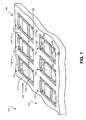
- FIG. 1 is a schematic diagram depicting a portion of a substrate including a representative arrangement of micromachines.
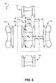
- FIG. 2 is a schematic diagram depicting the micromachines of FIG. 1.
- FIG. 3 is a schematic diagram depicting a representative arrangement of micromachines.
- FIG. 4 is a schematic diagram depicting a representative arrangement of micromachines.
- FIG. 5 is a schematic diagram depicting a portion of a substrate including an representative arrangement of micromachines.
- FIG. 1 depicts an embodiment of a micromachine system 100.
- embodiments of the micromachine system of the present invention can employ various techniques for providing high density packing of micromachines.
- micromachine system 100 includes multiple micromachines 110 that are provided on a substrate 111.
- substrate 111 can be a semiconductor wafer.
- Each micromachine 110 incorporates a micromover component ("micromover") 112.
- Micromovers 112 are adapted to move relative to at least a portion of substrate 111.
- various types of micromachines other than micromovers can be used.
- embodiments of the invention will be described with reference to micromovers. This is done merely for ease of description and not for the purpose of limitation.
- Micromovers 112 preferably are spaced from each other so that adjacent micromovers 112 do not interfere with each other. More specifically, if adjacent micromovers were permitted to contact each other, either or both of the micromovers could be inhibited from performing their intended functions and/or could be damaged. Spacing between adjacent micromachines is accommodated by arranging each micromover within a corresponding trench 116.
- each trench is defined by material of substrate 111. More specifically, the material of the substrate forms a longitudinal barrier 118 between adjacently disposed micromovers of a row 120 of micromovers. A transverse barrier 122 is formed between adjacently disposed micromovers of a column 124 of micromovers.
- Trenches 116 can be formed by either removing material of the substrate in the desired area of the trench, such as by etching, and/or by forming a raised area about the desired area of the trench, such as by deposition of material.
- micromovers 112 are substantially retained within their respective trenches by flexures 130.
- Multiple flexures 130 engage each micromover 112.
- the flexures tend to maintain a micromover within its trench while permitting the micromover to move, e.g. , micromover 112 moves relative to substrate 111.
- Representative examples of flexures include springs and micro-fabricated beams.
- Each flexure 130 is affixed to an anchor 132.
- Anchor 132 can be formed as a component affixed to the substrate or as a portion of the material of the substrate.
- Micromachines can be fabricated by a variety of micromachining processes.
- the device material is silicon that is provided in the form of a wafer.
- the micromover, flexure, and anchor system are defined in the silicon wafer by a masking layer, which can be formed of a photoresist, for example.
- a deep silicon reactive ion etch may be used to transfer the mask shape into the silicon wafer.
- a typical etch depth may be 10 to 100 ⁇ m.
- the etch depth is often set by an etch-stop layer that is provided in the silicon wafer before micromachining fabrication is begun.
- the etch-stop layer can be formed of silicon dioxide, for example.
- the etch-stop layer is used as a sacrificial layer to facilitate the release of the micromover from the substrate.
- Release refers to a process by which constraints on the MEMS part, e.g., the micromover, are removed. This allows the micromover to move freely relative to the substrate.
- flexures and anchors serve to constrain the motion of the released micromover to the desired degrees of freedom.
- An isotropic etch of the sacrificial layer is performed to remove the sacrificial material from about the micromachine components in desired areas.
- the sacrificial layer may be 1 ⁇ m thick, for example.
- the duration of the etch step will determine which structures are released from the substrate. For instance, the longer the etch time, the more sacrificial material typically is removed during the etch. By removing more material during the etch, typically a larger structure, i.e., the structure defined in the masking step, can be released. Given sufficient time, the release etch can completely remove sacrificial material formed underneath a micromover and its flexures. In contrast, anchors are not released by the etch. To prevent release of the anchors, the anchors are formed sufficiently wide so that they are not undercut by the etch to a degree that permits release.
- each micromachine 110 exhibits a length (M X ) and a width (M Y ), with M X and M Y including both the dimensions of the physical device and its operating range.
- M X and M Y including both the dimensions of the physical device and its operating range.
- Each micromachine 110 is spaced from an adjacent micromachine by a length (S X ), i.e. , S X is the distance between adjacent micromachines of the same row, and a width (S Y ), i.e. , S Y is the distance between adjacent micromachines of the same column.
- S X length
- S Y width
- the total area associated with a micromachine 110 is defined by: M X + (2)(1/2 S X ), in the X dimension; and M Y + (2)(1/2 S Y ), in the Y dimension.
- FIG. 3 An alternative embodiment of micromachine system 100 is depicted in FIG. 3. As shown in FIG. 3, longitudinal barriers, which are shown in the embodiment of FIGs. 1 and 2, are not provided between adjacent micromovers 110. In this configuration, an increased packing density of the micromachines is achieved compared to the embodiment of FIGs. 1 and 2. More specifically, each micromachine 110 of FIG. 3 requires a length of M X1 , i.e. , in some embodiments, M X1 ⁇ M X + (2)(1/2 S X ).
- separators 410 are provided between adjacently disposed micromachines.
- the separators 410 are adapted to prevent direct contact of adjacent micromovers.
- each separator 410 is formed as a distinct component, i.e. , the separator is not formed entirely of the material of the substrate.
- separator 410 could be a micro-fabricated beam that is similar to that of flexure 130.
- anchors 420 are used to secure multiple flexures 130.
- each anchor 420 is arranged between an adjacent pair of micromovers and is used to affix at least one flexure from each of the pair of micromovers.
- Each anchor 420 also can secure one or more separators 410.
- an increased packing density can be achieved. More specifically, in some embodiments, M X2 ⁇ M X1 ⁇ M X + (2)(1/2 S X ).
- micromachine system 100 includes multiple micromachines 502 that are provided on a substrate 504.
- Micromachines 502 preferably are spaced from each other so that adjacent micromovers 506 do not interfere with each other.
- Flexures 508 of the micromachines are affixed to anchors.
- the anchors being raised from a surface 510 of the substrate, define a trench 512 that is arranged about the anchors.
- anchors 514 are depicted, i.e. , anchors 514, 516, 518 and 520. More specifically, anchors 514 are adapted to affix a flexure from a single micromover. Typically, such a micromover is arranged at a corner of the array of micromachines. In regard to anchors 516, these anchors are adapted to affix flexures from at least two micromachines. Since micromachine system 100 of FIG. 5 includes columns 522 of micromachines, anchors 516 typically are provided only along the outer edge of a column of micromachines.
- Anchors 518 also are adapted to affix flexures from at least two micromovers. Anchors 518 typically are provided only along the outer edge of a row 524 of micromachines. Similar to anchors 516, anchors 518 are adapted to affix flexures from at least two micromachines. However, unlike anchors 516, each of which engages flexures on opposing sides of the anchor, each anchor 518 typically engages the flexures along one side of the anchor.
- Anchors 520 typically are provided at locations other than the outer periphery of an array of micromachines. As shown in FIG. 5, anchors 520 are adapted to affix flexures from at least four micromovers. In particular, one side of an anchor is adapted to affix flexures of adjacently disposed micromovers of a first row, and the other side of the anchor is adapted to affix flexures of adjacently disposed micromovers of a second row.
- separators also can be provided between at least some of the adjacently disposed micromovers of the micromachine system 100 depicted therein.
- spacing between adjacently disposed micromachines may not be required for micromachines that are intended to move together.
- a further increase in packing density can be achieved by configuring these micromachines so that they engage each other. All such modifications and variations are within the scope of the invention as determined by the appended claims when interpreted in accordance with the breadth to which they are fairly and legally entitled.
Landscapes
- Engineering & Computer Science (AREA)
- Computer Hardware Design (AREA)
- Microelectronics & Electronic Packaging (AREA)
- Micromachines (AREA)
Applications Claiming Priority (2)
| Application Number | Priority Date | Filing Date | Title |
|---|---|---|---|
| US923000 | 1992-07-29 | ||
| US09/923,000 US6600201B2 (en) | 2001-08-03 | 2001-08-03 | Systems with high density packing of micromachines |
Publications (2)
| Publication Number | Publication Date |
|---|---|
| EP1281665A2 true EP1281665A2 (fr) | 2003-02-05 |
| EP1281665A3 EP1281665A3 (fr) | 2005-02-16 |
Family
ID=25447947
Family Applications (1)
| Application Number | Title | Priority Date | Filing Date |
|---|---|---|---|
| EP02255271A Withdrawn EP1281665A3 (fr) | 2001-08-03 | 2002-07-29 | Systemes avec empaquetage à haute densité de microdispositifs |
Country Status (4)
| Country | Link |
|---|---|
| US (1) | US6600201B2 (fr) |
| EP (1) | EP1281665A3 (fr) |
| JP (1) | JP2003117898A (fr) |
| TW (1) | TW548776B (fr) |
Families Citing this family (167)
| Publication number | Priority date | Publication date | Assignee | Title |
|---|---|---|---|---|
| US6674562B1 (en) | 1994-05-05 | 2004-01-06 | Iridigm Display Corporation | Interferometric modulation of radiation |
| US7550794B2 (en) | 2002-09-20 | 2009-06-23 | Idc, Llc | Micromechanical systems device comprising a displaceable electrode and a charge-trapping layer |
| US7297471B1 (en) | 2003-04-15 | 2007-11-20 | Idc, Llc | Method for manufacturing an array of interferometric modulators |
| US7123216B1 (en) | 1994-05-05 | 2006-10-17 | Idc, Llc | Photonic MEMS and structures |
| US8014059B2 (en) | 1994-05-05 | 2011-09-06 | Qualcomm Mems Technologies, Inc. | System and method for charge control in a MEMS device |
| US7138984B1 (en) | 2001-06-05 | 2006-11-21 | Idc, Llc | Directly laminated touch sensitive screen |
| US7460291B2 (en) | 1994-05-05 | 2008-12-02 | Idc, Llc | Separable modulator |
| US6680792B2 (en) | 1994-05-05 | 2004-01-20 | Iridigm Display Corporation | Interferometric modulation of radiation |
| US7471444B2 (en) | 1996-12-19 | 2008-12-30 | Idc, Llc | Interferometric modulation of radiation |
| US8928967B2 (en) | 1998-04-08 | 2015-01-06 | Qualcomm Mems Technologies, Inc. | Method and device for modulating light |
| US7532377B2 (en) | 1998-04-08 | 2009-05-12 | Idc, Llc | Movable micro-electromechanical device |
| WO1999052006A2 (fr) | 1998-04-08 | 1999-10-14 | Etalon, Inc. | Modulation interferometrique de rayonnement |
| WO2003007049A1 (fr) | 1999-10-05 | 2003-01-23 | Iridigm Display Corporation | Mems et structures photoniques |
| US6962771B1 (en) * | 2000-10-13 | 2005-11-08 | Taiwan Semiconductor Manufacturing Company, Ltd. | Dual damascene process |
| US6589625B1 (en) * | 2001-08-01 | 2003-07-08 | Iridigm Display Corporation | Hermetic seal and method to create the same |
| US6794119B2 (en) | 2002-02-12 | 2004-09-21 | Iridigm Display Corporation | Method for fabricating a structure for a microelectromechanical systems (MEMS) device |
| US6574033B1 (en) | 2002-02-27 | 2003-06-03 | Iridigm Display Corporation | Microelectromechanical systems device and method for fabricating same |
| US7781850B2 (en) | 2002-09-20 | 2010-08-24 | Qualcomm Mems Technologies, Inc. | Controlling electromechanical behavior of structures within a microelectromechanical systems device |
| TW200413810A (en) | 2003-01-29 | 2004-08-01 | Prime View Int Co Ltd | Light interference display panel and its manufacturing method |
| TW594360B (en) | 2003-04-21 | 2004-06-21 | Prime View Int Corp Ltd | A method for fabricating an interference display cell |
| TW570896B (en) | 2003-05-26 | 2004-01-11 | Prime View Int Co Ltd | A method for fabricating an interference display cell |
| US7221495B2 (en) | 2003-06-24 | 2007-05-22 | Idc Llc | Thin film precursor stack for MEMS manufacturing |
| TWI231865B (en) | 2003-08-26 | 2005-05-01 | Prime View Int Co Ltd | An interference display cell and fabrication method thereof |
| TW593126B (en) | 2003-09-30 | 2004-06-21 | Prime View Int Co Ltd | A structure of a micro electro mechanical system and manufacturing the same |
| US7012726B1 (en) | 2003-11-03 | 2006-03-14 | Idc, Llc | MEMS devices with unreleased thin film components |
| US7161728B2 (en) | 2003-12-09 | 2007-01-09 | Idc, Llc | Area array modulation and lead reduction in interferometric modulators |
| US7142346B2 (en) | 2003-12-09 | 2006-11-28 | Idc, Llc | System and method for addressing a MEMS display |
| US7532194B2 (en) | 2004-02-03 | 2009-05-12 | Idc, Llc | Driver voltage adjuster |
| US7026189B2 (en) * | 2004-02-11 | 2006-04-11 | Hewlett-Packard Development Company, L.P. | Wafer packaging and singulation method |
| US7119945B2 (en) | 2004-03-03 | 2006-10-10 | Idc, Llc | Altering temporal response of microelectromechanical elements |
| US7706050B2 (en) | 2004-03-05 | 2010-04-27 | Qualcomm Mems Technologies, Inc. | Integrated modulator illumination |
| US7476327B2 (en) | 2004-05-04 | 2009-01-13 | Idc, Llc | Method of manufacture for microelectromechanical devices |
| US7060895B2 (en) | 2004-05-04 | 2006-06-13 | Idc, Llc | Modifying the electro-mechanical behavior of devices |
| US7164520B2 (en) | 2004-05-12 | 2007-01-16 | Idc, Llc | Packaging for an interferometric modulator |
| US7256922B2 (en) | 2004-07-02 | 2007-08-14 | Idc, Llc | Interferometric modulators with thin film transistors |
| WO2006014929A1 (fr) | 2004-07-29 | 2006-02-09 | Idc, Llc | Systeme et procede pour le fonctionnement micro-electromecanique d'un modulateur interferometrique |
| US7551159B2 (en) | 2004-08-27 | 2009-06-23 | Idc, Llc | System and method of sensing actuation and release voltages of an interferometric modulator |
| US7560299B2 (en) | 2004-08-27 | 2009-07-14 | Idc, Llc | Systems and methods of actuating MEMS display elements |
| US7515147B2 (en) | 2004-08-27 | 2009-04-07 | Idc, Llc | Staggered column drive circuit systems and methods |
| US7889163B2 (en) | 2004-08-27 | 2011-02-15 | Qualcomm Mems Technologies, Inc. | Drive method for MEMS devices |
| US7499208B2 (en) | 2004-08-27 | 2009-03-03 | Udc, Llc | Current mode display driver circuit realization feature |
| US7602375B2 (en) | 2004-09-27 | 2009-10-13 | Idc, Llc | Method and system for writing data to MEMS display elements |
| US7369294B2 (en) | 2004-09-27 | 2008-05-06 | Idc, Llc | Ornamental display device |
| US7369296B2 (en) | 2004-09-27 | 2008-05-06 | Idc, Llc | Device and method for modifying actuation voltage thresholds of a deformable membrane in an interferometric modulator |
| US7545550B2 (en) | 2004-09-27 | 2009-06-09 | Idc, Llc | Systems and methods of actuating MEMS display elements |
| US7564612B2 (en) | 2004-09-27 | 2009-07-21 | Idc, Llc | Photonic MEMS and structures |
| US7372613B2 (en) | 2004-09-27 | 2008-05-13 | Idc, Llc | Method and device for multistate interferometric light modulation |
| US7936497B2 (en) | 2004-09-27 | 2011-05-03 | Qualcomm Mems Technologies, Inc. | MEMS device having deformable membrane characterized by mechanical persistence |
| US7368803B2 (en) | 2004-09-27 | 2008-05-06 | Idc, Llc | System and method for protecting microelectromechanical systems array using back-plate with non-flat portion |
| CN100439967C (zh) | 2004-09-27 | 2008-12-03 | Idc公司 | 用于多状态干涉光调制的方法和设备 |
| US7527995B2 (en) | 2004-09-27 | 2009-05-05 | Qualcomm Mems Technologies, Inc. | Method of making prestructure for MEMS systems |
| US8008736B2 (en) | 2004-09-27 | 2011-08-30 | Qualcomm Mems Technologies, Inc. | Analog interferometric modulator device |
| US7304784B2 (en) | 2004-09-27 | 2007-12-04 | Idc, Llc | Reflective display device having viewable display on both sides |
| US7583429B2 (en) | 2004-09-27 | 2009-09-01 | Idc, Llc | Ornamental display device |
| US7532195B2 (en) | 2004-09-27 | 2009-05-12 | Idc, Llc | Method and system for reducing power consumption in a display |
| US7259449B2 (en) | 2004-09-27 | 2007-08-21 | Idc, Llc | Method and system for sealing a substrate |
| US7327510B2 (en) | 2004-09-27 | 2008-02-05 | Idc, Llc | Process for modifying offset voltage characteristics of an interferometric modulator |
| US7321456B2 (en) | 2004-09-27 | 2008-01-22 | Idc, Llc | Method and device for corner interferometric modulation |
| US7349136B2 (en) | 2004-09-27 | 2008-03-25 | Idc, Llc | Method and device for a display having transparent components integrated therein |
| US7668415B2 (en) | 2004-09-27 | 2010-02-23 | Qualcomm Mems Technologies, Inc. | Method and device for providing electronic circuitry on a backplate |
| US7355780B2 (en) | 2004-09-27 | 2008-04-08 | Idc, Llc | System and method of illuminating interferometric modulators using backlighting |
| US8878825B2 (en) | 2004-09-27 | 2014-11-04 | Qualcomm Mems Technologies, Inc. | System and method for providing a variable refresh rate of an interferometric modulator display |
| US7424198B2 (en) | 2004-09-27 | 2008-09-09 | Idc, Llc | Method and device for packaging a substrate |
| US8124434B2 (en) | 2004-09-27 | 2012-02-28 | Qualcomm Mems Technologies, Inc. | Method and system for packaging a display |
| US7808703B2 (en) | 2004-09-27 | 2010-10-05 | Qualcomm Mems Technologies, Inc. | System and method for implementation of interferometric modulator displays |
| US7630119B2 (en) | 2004-09-27 | 2009-12-08 | Qualcomm Mems Technologies, Inc. | Apparatus and method for reducing slippage between structures in an interferometric modulator |
| US7553684B2 (en) | 2004-09-27 | 2009-06-30 | Idc, Llc | Method of fabricating interferometric devices using lift-off processing techniques |
| US7944599B2 (en) | 2004-09-27 | 2011-05-17 | Qualcomm Mems Technologies, Inc. | Electromechanical device with optical function separated from mechanical and electrical function |
| US7710629B2 (en) | 2004-09-27 | 2010-05-04 | Qualcomm Mems Technologies, Inc. | System and method for display device with reinforcing substance |
| US7317568B2 (en) | 2004-09-27 | 2008-01-08 | Idc, Llc | System and method of implementation of interferometric modulators for display mirrors |
| US7692839B2 (en) | 2004-09-27 | 2010-04-06 | Qualcomm Mems Technologies, Inc. | System and method of providing MEMS device with anti-stiction coating |
| US7130104B2 (en) | 2004-09-27 | 2006-10-31 | Idc, Llc | Methods and devices for inhibiting tilting of a mirror in an interferometric modulator |
| US7405924B2 (en) | 2004-09-27 | 2008-07-29 | Idc, Llc | System and method for protecting microelectromechanical systems array using structurally reinforced back-plate |
| US7373026B2 (en) * | 2004-09-27 | 2008-05-13 | Idc, Llc | MEMS device fabricated on a pre-patterned substrate |
| US7302157B2 (en) | 2004-09-27 | 2007-11-27 | Idc, Llc | System and method for multi-level brightness in interferometric modulation |
| US7343080B2 (en) | 2004-09-27 | 2008-03-11 | Idc, Llc | System and method of testing humidity in a sealed MEMS device |
| US7161730B2 (en) | 2004-09-27 | 2007-01-09 | Idc, Llc | System and method for providing thermal compensation for an interferometric modulator display |
| US7626581B2 (en) | 2004-09-27 | 2009-12-01 | Idc, Llc | Device and method for display memory using manipulation of mechanical response |
| US20060176487A1 (en) | 2004-09-27 | 2006-08-10 | William Cummings | Process control monitors for interferometric modulators |
| US7420725B2 (en) | 2004-09-27 | 2008-09-02 | Idc, Llc | Device having a conductive light absorbing mask and method for fabricating same |
| US7289259B2 (en) | 2004-09-27 | 2007-10-30 | Idc, Llc | Conductive bus structure for interferometric modulator array |
| US7417735B2 (en) | 2004-09-27 | 2008-08-26 | Idc, Llc | Systems and methods for measuring color and contrast in specular reflective devices |
| US7429334B2 (en) | 2004-09-27 | 2008-09-30 | Idc, Llc | Methods of fabricating interferometric modulators by selectively removing a material |
| US7345805B2 (en) | 2004-09-27 | 2008-03-18 | Idc, Llc | Interferometric modulator array with integrated MEMS electrical switches |
| US7843410B2 (en) | 2004-09-27 | 2010-11-30 | Qualcomm Mems Technologies, Inc. | Method and device for electrically programmable display |
| US7289256B2 (en) | 2004-09-27 | 2007-10-30 | Idc, Llc | Electrical characterization of interferometric modulators |
| US7893919B2 (en) | 2004-09-27 | 2011-02-22 | Qualcomm Mems Technologies, Inc. | Display region architectures |
| US7136213B2 (en) | 2004-09-27 | 2006-11-14 | Idc, Llc | Interferometric modulators having charge persistence |
| US7701631B2 (en) | 2004-09-27 | 2010-04-20 | Qualcomm Mems Technologies, Inc. | Device having patterned spacers for backplates and method of making the same |
| US7679627B2 (en) | 2004-09-27 | 2010-03-16 | Qualcomm Mems Technologies, Inc. | Controller and driver features for bi-stable display |
| US7359066B2 (en) | 2004-09-27 | 2008-04-15 | Idc, Llc | Electro-optical measurement of hysteresis in interferometric modulators |
| US7653371B2 (en) | 2004-09-27 | 2010-01-26 | Qualcomm Mems Technologies, Inc. | Selectable capacitance circuit |
| US7684104B2 (en) | 2004-09-27 | 2010-03-23 | Idc, Llc | MEMS using filler material and method |
| US8310441B2 (en) | 2004-09-27 | 2012-11-13 | Qualcomm Mems Technologies, Inc. | Method and system for writing data to MEMS display elements |
| US20060076634A1 (en) | 2004-09-27 | 2006-04-13 | Lauren Palmateer | Method and system for packaging MEMS devices with incorporated getter |
| US7492502B2 (en) | 2004-09-27 | 2009-02-17 | Idc, Llc | Method of fabricating a free-standing microstructure |
| US7415186B2 (en) | 2004-09-27 | 2008-08-19 | Idc, Llc | Methods for visually inspecting interferometric modulators for defects |
| US7417783B2 (en) | 2004-09-27 | 2008-08-26 | Idc, Llc | Mirror and mirror layer for optical modulator and method |
| US7446927B2 (en) | 2004-09-27 | 2008-11-04 | Idc, Llc | MEMS switch with set and latch electrodes |
| US7813026B2 (en) | 2004-09-27 | 2010-10-12 | Qualcomm Mems Technologies, Inc. | System and method of reducing color shift in a display |
| US7920135B2 (en) | 2004-09-27 | 2011-04-05 | Qualcomm Mems Technologies, Inc. | Method and system for driving a bi-stable display |
| US7586484B2 (en) | 2004-09-27 | 2009-09-08 | Idc, Llc | Controller and driver features for bi-stable display |
| US7675669B2 (en) | 2004-09-27 | 2010-03-09 | Qualcomm Mems Technologies, Inc. | Method and system for driving interferometric modulators |
| US7724993B2 (en) | 2004-09-27 | 2010-05-25 | Qualcomm Mems Technologies, Inc. | MEMS switches with deforming membranes |
| US7719500B2 (en) | 2004-09-27 | 2010-05-18 | Qualcomm Mems Technologies, Inc. | Reflective display pixels arranged in non-rectangular arrays |
| US7299681B2 (en) | 2004-09-27 | 2007-11-27 | Idc, Llc | Method and system for detecting leak in electronic devices |
| US7916103B2 (en) | 2004-09-27 | 2011-03-29 | Qualcomm Mems Technologies, Inc. | System and method for display device with end-of-life phenomena |
| US7310179B2 (en) | 2004-09-27 | 2007-12-18 | Idc, Llc | Method and device for selective adjustment of hysteresis window |
| US7554714B2 (en) | 2004-09-27 | 2009-06-30 | Idc, Llc | Device and method for manipulation of thermal response in a modulator |
| US7453579B2 (en) | 2004-09-27 | 2008-11-18 | Idc, Llc | Measurement of the dynamic characteristics of interferometric modulators |
| US7405861B2 (en) | 2004-09-27 | 2008-07-29 | Idc, Llc | Method and device for protecting interferometric modulators from electrostatic discharge |
| US7460246B2 (en) | 2004-09-27 | 2008-12-02 | Idc, Llc | Method and system for sensing light using interferometric elements |
| US7535466B2 (en) | 2004-09-27 | 2009-05-19 | Idc, Llc | System with server based control of client device display features |
| US7422962B2 (en) * | 2004-10-27 | 2008-09-09 | Hewlett-Packard Development Company, L.P. | Method of singulating electronic devices |
| US7503989B2 (en) * | 2004-12-17 | 2009-03-17 | Hewlett-Packard Development Company, L.P. | Methods and systems for aligning and coupling devices |
| TW200628877A (en) | 2005-02-04 | 2006-08-16 | Prime View Int Co Ltd | Method of manufacturing optical interference type color display |
| US7920136B2 (en) | 2005-05-05 | 2011-04-05 | Qualcomm Mems Technologies, Inc. | System and method of driving a MEMS display device |
| CA2607807A1 (fr) | 2005-05-05 | 2006-11-16 | Qualcomm Incorporated | Circuit integre pilote dynamique et configuration de panneau afficheur |
| US7948457B2 (en) | 2005-05-05 | 2011-05-24 | Qualcomm Mems Technologies, Inc. | Systems and methods of actuating MEMS display elements |
| JP2009503564A (ja) | 2005-07-22 | 2009-01-29 | クアルコム,インコーポレイテッド | Memsデバイスのための支持構造、およびその方法 |
| RU2468988C2 (ru) | 2005-07-22 | 2012-12-10 | Квалкомм Инкорпорэйтэд | Устройства мэмс, имеющие поддерживающие структуры, и способы их изготовления |
| EP2495212A3 (fr) * | 2005-07-22 | 2012-10-31 | QUALCOMM MEMS Technologies, Inc. | Dispositifs MEMS comportant des structures de support et procédés de fabrication associés |
| US7355779B2 (en) | 2005-09-02 | 2008-04-08 | Idc, Llc | Method and system for driving MEMS display elements |
| US7580172B2 (en) | 2005-09-30 | 2009-08-25 | Qualcomm Mems Technologies, Inc. | MEMS device and interconnects for same |
| US7630114B2 (en) | 2005-10-28 | 2009-12-08 | Idc, Llc | Diffusion barrier layer for MEMS devices |
| US8391630B2 (en) | 2005-12-22 | 2013-03-05 | Qualcomm Mems Technologies, Inc. | System and method for power reduction when decompressing video streams for interferometric modulator displays |
| US7795061B2 (en) | 2005-12-29 | 2010-09-14 | Qualcomm Mems Technologies, Inc. | Method of creating MEMS device cavities by a non-etching process |
| US7636151B2 (en) | 2006-01-06 | 2009-12-22 | Qualcomm Mems Technologies, Inc. | System and method for providing residual stress test structures |
| US7916980B2 (en) | 2006-01-13 | 2011-03-29 | Qualcomm Mems Technologies, Inc. | Interconnect structure for MEMS device |
| US7382515B2 (en) | 2006-01-18 | 2008-06-03 | Qualcomm Mems Technologies, Inc. | Silicon-rich silicon nitrides as etch stops in MEMS manufacture |
| US7652814B2 (en) | 2006-01-27 | 2010-01-26 | Qualcomm Mems Technologies, Inc. | MEMS device with integrated optical element |
| US8194056B2 (en) | 2006-02-09 | 2012-06-05 | Qualcomm Mems Technologies Inc. | Method and system for writing data to MEMS display elements |
| US7582952B2 (en) | 2006-02-21 | 2009-09-01 | Qualcomm Mems Technologies, Inc. | Method for providing and removing discharging interconnect for chip-on-glass output leads and structures thereof |
| US7547568B2 (en) | 2006-02-22 | 2009-06-16 | Qualcomm Mems Technologies, Inc. | Electrical conditioning of MEMS device and insulating layer thereof |
| US7550810B2 (en) | 2006-02-23 | 2009-06-23 | Qualcomm Mems Technologies, Inc. | MEMS device having a layer movable at asymmetric rates |
| US7450295B2 (en) * | 2006-03-02 | 2008-11-11 | Qualcomm Mems Technologies, Inc. | Methods for producing MEMS with protective coatings using multi-component sacrificial layers |
| US7643203B2 (en) * | 2006-04-10 | 2010-01-05 | Qualcomm Mems Technologies, Inc. | Interferometric optical display system with broadband characteristics |
| US7903047B2 (en) | 2006-04-17 | 2011-03-08 | Qualcomm Mems Technologies, Inc. | Mode indicator for interferometric modulator displays |
| US7711239B2 (en) | 2006-04-19 | 2010-05-04 | Qualcomm Mems Technologies, Inc. | Microelectromechanical device and method utilizing nanoparticles |
| US7527996B2 (en) | 2006-04-19 | 2009-05-05 | Qualcomm Mems Technologies, Inc. | Non-planar surface structures and process for microelectromechanical systems |
| US7417784B2 (en) | 2006-04-19 | 2008-08-26 | Qualcomm Mems Technologies, Inc. | Microelectromechanical device and method utilizing a porous surface |
| US7623287B2 (en) | 2006-04-19 | 2009-11-24 | Qualcomm Mems Technologies, Inc. | Non-planar surface structures and process for microelectromechanical systems |
| US8049713B2 (en) | 2006-04-24 | 2011-11-01 | Qualcomm Mems Technologies, Inc. | Power consumption optimized display update |
| US7369292B2 (en) * | 2006-05-03 | 2008-05-06 | Qualcomm Mems Technologies, Inc. | Electrode and interconnect materials for MEMS devices |
| US7649671B2 (en) | 2006-06-01 | 2010-01-19 | Qualcomm Mems Technologies, Inc. | Analog interferometric modulator device with electrostatic actuation and release |
| US7405863B2 (en) | 2006-06-01 | 2008-07-29 | Qualcomm Mems Technologies, Inc. | Patterning of mechanical layer in MEMS to reduce stresses at supports |
| US7321457B2 (en) | 2006-06-01 | 2008-01-22 | Qualcomm Incorporated | Process and structure for fabrication of MEMS device having isolated edge posts |
| US7471442B2 (en) | 2006-06-15 | 2008-12-30 | Qualcomm Mems Technologies, Inc. | Method and apparatus for low range bit depth enhancements for MEMS display architectures |
| US7702192B2 (en) | 2006-06-21 | 2010-04-20 | Qualcomm Mems Technologies, Inc. | Systems and methods for driving MEMS display |
| US7835061B2 (en) | 2006-06-28 | 2010-11-16 | Qualcomm Mems Technologies, Inc. | Support structures for free-standing electromechanical devices |
| US7385744B2 (en) | 2006-06-28 | 2008-06-10 | Qualcomm Mems Technologies, Inc. | Support structure for free-standing MEMS device and methods for forming the same |
| US7777715B2 (en) | 2006-06-29 | 2010-08-17 | Qualcomm Mems Technologies, Inc. | Passive circuits for de-multiplexing display inputs |
| US7527998B2 (en) | 2006-06-30 | 2009-05-05 | Qualcomm Mems Technologies, Inc. | Method of manufacturing MEMS devices providing air gap control |
| US7388704B2 (en) | 2006-06-30 | 2008-06-17 | Qualcomm Mems Technologies, Inc. | Determination of interferometric modulator mirror curvature and airgap variation using digital photographs |
| US7566664B2 (en) | 2006-08-02 | 2009-07-28 | Qualcomm Mems Technologies, Inc. | Selective etching of MEMS using gaseous halides and reactive co-etchants |
| US7763546B2 (en) | 2006-08-02 | 2010-07-27 | Qualcomm Mems Technologies, Inc. | Methods for reducing surface charges during the manufacture of microelectromechanical systems devices |
| US7706042B2 (en) | 2006-12-20 | 2010-04-27 | Qualcomm Mems Technologies, Inc. | MEMS device and interconnects for same |
| US7535621B2 (en) | 2006-12-27 | 2009-05-19 | Qualcomm Mems Technologies, Inc. | Aluminum fluoride films for microelectromechanical system applications |
| US7733552B2 (en) | 2007-03-21 | 2010-06-08 | Qualcomm Mems Technologies, Inc | MEMS cavity-coating layers and methods |
| US7719752B2 (en) | 2007-05-11 | 2010-05-18 | Qualcomm Mems Technologies, Inc. | MEMS structures, methods of fabricating MEMS components on separate substrates and assembly of same |
| US7570415B2 (en) | 2007-08-07 | 2009-08-04 | Qualcomm Mems Technologies, Inc. | MEMS device and interconnects for same |
| US7864403B2 (en) | 2009-03-27 | 2011-01-04 | Qualcomm Mems Technologies, Inc. | Post-release adjustment of interferometric modulator reflectivity |
| US8736590B2 (en) | 2009-03-27 | 2014-05-27 | Qualcomm Mems Technologies, Inc. | Low voltage driver scheme for interferometric modulators |
| KR20130100232A (ko) | 2010-04-09 | 2013-09-10 | 퀄컴 엠이엠에스 테크놀로지스, 인크. | 전기 기계 디바이스의 기계층 및 그 형성 방법 |
| US8963159B2 (en) | 2011-04-04 | 2015-02-24 | Qualcomm Mems Technologies, Inc. | Pixel via and methods of forming the same |
| US9134527B2 (en) | 2011-04-04 | 2015-09-15 | Qualcomm Mems Technologies, Inc. | Pixel via and methods of forming the same |
| CN108178121B (zh) * | 2018-02-07 | 2024-05-03 | 北京先通康桥医药科技有限公司 | 触诊探头及其制造方法 |
Citations (1)
| Publication number | Priority date | Publication date | Assignee | Title |
|---|---|---|---|---|
| US5999306A (en) | 1995-12-01 | 1999-12-07 | Seiko Epson Corporation | Method of manufacturing spatial light modulator and electronic device employing it |
Family Cites Families (1)
| Publication number | Priority date | Publication date | Assignee | Title |
|---|---|---|---|---|
| US6211598B1 (en) * | 1999-09-13 | 2001-04-03 | Jds Uniphase Inc. | In-plane MEMS thermal actuator and associated fabrication methods |
-
2001
- 2001-08-03 US US09/923,000 patent/US6600201B2/en not_active Expired - Fee Related
-
2002
- 2002-07-11 TW TW091115463A patent/TW548776B/zh not_active IP Right Cessation
- 2002-07-29 EP EP02255271A patent/EP1281665A3/fr not_active Withdrawn
- 2002-07-30 JP JP2002221120A patent/JP2003117898A/ja active Pending
Patent Citations (1)
| Publication number | Priority date | Publication date | Assignee | Title |
|---|---|---|---|---|
| US5999306A (en) | 1995-12-01 | 1999-12-07 | Seiko Epson Corporation | Method of manufacturing spatial light modulator and electronic device employing it |
Non-Patent Citations (3)
| Title |
|---|
| HILLER K ET AL.: "Low temperature approaches for fabrication of high-frequency microscanners", PROCEEDINGS OF THE SPIE, MINITURIZED SYSTEMS WITH MICRO-OPTICS AND MEMS, vol. 3878, 20 September 1999 (1999-09-20), pages 58 - 66 |
| KURTH S ET AL.: "Silicon morrors and micromirror arrays for spatial laser beam modulation", SENSORS AND ACTUATORS A, ELSEVIER SEQUOIA S.A., LAUSANNE, vol. 66, no. 1-3, 1 April 1998 (1998-04-01), pages 76 - 82 |
| KURTH S ET AL.: "Synchronously working micromirrors for beam steering: design and application aspects", PROCEEDINGS OF THE SPIE, OPTICAL SCANNING DESIGN AND APPLICATION, vol. 3787, 21 July 1999 (1999-07-21), pages 63 - 73 |
Also Published As
| Publication number | Publication date |
|---|---|
| JP2003117898A (ja) | 2003-04-23 |
| US20030025168A1 (en) | 2003-02-06 |
| TW548776B (en) | 2003-08-21 |
| US6600201B2 (en) | 2003-07-29 |
| EP1281665A3 (fr) | 2005-02-16 |
Similar Documents
| Publication | Publication Date | Title |
|---|---|---|
| US6600201B2 (en) | Systems with high density packing of micromachines | |
| US6953704B2 (en) | Systems with high density packing of micromachines | |
| KR100421217B1 (ko) | 점착 방지 미세 구조물 제조 방법 | |
| US6573156B1 (en) | Low defect method for die singulation and for structural support for handling thin film devices | |
| US7068417B2 (en) | Method and apparatus for a reflective spatial light modulator with a flexible pedestal | |
| JP4431502B2 (ja) | エピタキシによって半導体デバイスを形成する方法 | |
| US7026184B2 (en) | Method of fabricating microstructures and devices made therefrom | |
| US6767614B1 (en) | Multiple-level actuators and clamping devices | |
| US6694504B2 (en) | Method of fabricating an electrostatic vertical and torsional actuator using one single-crystalline silicon wafer | |
| WO2005118914A2 (fr) | Systeme et procede de support de substrat | |
| EP1062685A1 (fr) | Microstructures de grande superficie et dispositifs micromecaniques integres | |
| WO2003034469A2 (fr) | Procede de fabrication d'un dispositif possedant une surface ou un profil recherche non plan et dispositif produit par ce procede | |
| US8705159B2 (en) | Microelectromechanical system with a center of mass balanced by a mirror substrate | |
| US6756247B1 (en) | Integrated large area microstructures and micromechanical devices | |
| US6544863B1 (en) | Method of fabricating semiconductor wafers having multiple height subsurface layers | |
| US20120286378A1 (en) | Microelectromechanical system with balanced center of mass | |
| US6875257B2 (en) | Particle filter for microelectromechanical systems | |
| Keller | Microfabricated silicon high aspect ratio flexures for in-plane motion | |
| US6846087B2 (en) | Micromirror having counterbalancing structures and method for manufacturing same | |
| US6707077B2 (en) | Chip interconnect bus | |
| US6938487B2 (en) | Inertia sensor | |
| KR101374057B1 (ko) | 3차원 mems 구조체 및 그 제조 방법 | |
| Lee | Two-depth, single crystal silicon microelectromechanical systems | |
| JP4353006B2 (ja) | 半導体構造の製造方法 | |
| US6706619B2 (en) | Method for tiling unit cells |
Legal Events
| Date | Code | Title | Description |
|---|---|---|---|
| PUAI | Public reference made under article 153(3) epc to a published international application that has entered the european phase |
Free format text: ORIGINAL CODE: 0009012 |
|
| AK | Designated contracting states |
Designated state(s): AT BE BG CH CY CZ DE DK EE ES FI FR GB GR IE IT LI LU MC NL PT SE SK TR |
|
| AX | Request for extension of the european patent |
Extension state: AL LT LV MK RO SI |
|
| PUAL | Search report despatched |
Free format text: ORIGINAL CODE: 0009013 |
|
| AK | Designated contracting states |
Kind code of ref document: A3 Designated state(s): AT BE BG CH CY CZ DE DK EE ES FI FR GB GR IE IT LI LU MC NL PT SE SK TR |
|
| AX | Request for extension of the european patent |
Extension state: AL LT LV MK RO SI |
|
| 17P | Request for examination filed |
Effective date: 20050728 |
|
| AKX | Designation fees paid |
Designated state(s): DE FR IT |
|
| 17Q | First examination report despatched |
Effective date: 20080903 |
|
| STAA | Information on the status of an ep patent application or granted ep patent |
Free format text: STATUS: THE APPLICATION IS DEEMED TO BE WITHDRAWN |
|
| 18D | Application deemed to be withdrawn |
Effective date: 20110201 |