EP1282011B1 - Lentille de projection réflective pour la photolithographie dans l'ultraviolet extrême - Google Patents
Lentille de projection réflective pour la photolithographie dans l'ultraviolet extrême Download PDFInfo
- Publication number
- EP1282011B1 EP1282011B1 EP02016693A EP02016693A EP1282011B1 EP 1282011 B1 EP1282011 B1 EP 1282011B1 EP 02016693 A EP02016693 A EP 02016693A EP 02016693 A EP02016693 A EP 02016693A EP 1282011 B1 EP1282011 B1 EP 1282011B1
- Authority
- EP
- European Patent Office
- Prior art keywords
- mirror
- mirrors
- projection objective
- graded
- decentred
- Prior art date
- Legal status (The legal status is an assumption and is not a legal conclusion. Google has not performed a legal analysis and makes no representation as to the accuracy of the status listed.)
- Expired - Lifetime
Links
- 238000000206 photolithography Methods 0.000 title description 2
- 238000000576 coating method Methods 0.000 claims description 84
- 239000011248 coating agent Substances 0.000 claims description 42
- 210000001747 pupil Anatomy 0.000 claims description 35
- 230000003287 optical effect Effects 0.000 claims description 27
- 238000003384 imaging method Methods 0.000 claims description 16
- 230000005855 radiation Effects 0.000 claims description 14
- 230000005670 electromagnetic radiation Effects 0.000 claims description 7
- 230000004075 alteration Effects 0.000 claims description 5
- 230000005540 biological transmission Effects 0.000 description 31
- 238000009826 distribution Methods 0.000 description 25
- 239000000758 substrate Substances 0.000 description 15
- 238000000034 method Methods 0.000 description 10
- 230000000694 effects Effects 0.000 description 9
- 238000010586 diagram Methods 0.000 description 7
- 238000005457 optimization Methods 0.000 description 7
- 238000002310 reflectometry Methods 0.000 description 6
- 238000001900 extreme ultraviolet lithography Methods 0.000 description 4
- 230000002349 favourable effect Effects 0.000 description 4
- 238000005286 illumination Methods 0.000 description 4
- 238000004519 manufacturing process Methods 0.000 description 4
- ZOKXTWBITQBERF-UHFFFAOYSA-N Molybdenum Chemical compound [Mo] ZOKXTWBITQBERF-UHFFFAOYSA-N 0.000 description 2
- XUIMIQQOPSSXEZ-UHFFFAOYSA-N Silicon Chemical compound [Si] XUIMIQQOPSSXEZ-UHFFFAOYSA-N 0.000 description 2
- 230000001419 dependent effect Effects 0.000 description 2
- 230000006866 deterioration Effects 0.000 description 2
- 239000000463 material Substances 0.000 description 2
- 229910052750 molybdenum Inorganic materials 0.000 description 2
- 239000011733 molybdenum Substances 0.000 description 2
- 229910052710 silicon Inorganic materials 0.000 description 2
- 239000010703 silicon Substances 0.000 description 2
- 230000002411 adverse Effects 0.000 description 1
- 238000010276 construction Methods 0.000 description 1
- 230000007423 decrease Effects 0.000 description 1
- 230000002950 deficient Effects 0.000 description 1
- 238000005516 engineering process Methods 0.000 description 1
- 239000004973 liquid crystal related substance Substances 0.000 description 1
- 238000001393 microlithography Methods 0.000 description 1
- 229920002120 photoresistant polymer Polymers 0.000 description 1
- 230000008092 positive effect Effects 0.000 description 1
- 239000004065 semiconductor Substances 0.000 description 1
- 230000003068 static effect Effects 0.000 description 1
- 238000009827 uniform distribution Methods 0.000 description 1
Images

Classifications
-
- G—PHYSICS
- G03—PHOTOGRAPHY; CINEMATOGRAPHY; ANALOGOUS TECHNIQUES USING WAVES OTHER THAN OPTICAL WAVES; ELECTROGRAPHY; HOLOGRAPHY
- G03F—PHOTOMECHANICAL PRODUCTION OF TEXTURED OR PATTERNED SURFACES, e.g. FOR PRINTING, FOR PROCESSING OF SEMICONDUCTOR DEVICES; MATERIALS THEREFOR; ORIGINALS THEREFOR; APPARATUS SPECIALLY ADAPTED THEREFOR
- G03F7/00—Photomechanical, e.g. photolithographic, production of textured or patterned surfaces, e.g. printing surfaces; Materials therefor, e.g. comprising photoresists; Apparatus specially adapted therefor
- G03F7/70—Microphotolithographic exposure; Apparatus therefor
- G03F7/70216—Mask projection systems
- G03F7/70233—Optical aspects of catoptric systems, i.e. comprising only reflective elements, e.g. extreme ultraviolet [EUV] projection systems
-
- G—PHYSICS
- G02—OPTICS
- G02B—OPTICAL ELEMENTS, SYSTEMS OR APPARATUS
- G02B17/00—Systems with reflecting surfaces, with or without refracting elements
- G02B17/02—Catoptric systems, e.g. image erecting and reversing system
- G02B17/06—Catoptric systems, e.g. image erecting and reversing system using mirrors only, i.e. having only one curved mirror
- G02B17/0647—Catoptric systems, e.g. image erecting and reversing system using mirrors only, i.e. having only one curved mirror using more than three curved mirrors
- G02B17/0657—Catoptric systems, e.g. image erecting and reversing system using mirrors only, i.e. having only one curved mirror using more than three curved mirrors off-axis or unobscured systems in which all of the mirrors share a common axis of rotational symmetry
-
- G—PHYSICS
- G02—OPTICS
- G02B—OPTICAL ELEMENTS, SYSTEMS OR APPARATUS
- G02B5/00—Optical elements other than lenses
- G02B5/08—Mirrors
- G02B5/0891—Ultraviolet [UV] mirrors
-
- G—PHYSICS
- G02—OPTICS
- G02B—OPTICAL ELEMENTS, SYSTEMS OR APPARATUS
- G02B5/00—Optical elements other than lenses
- G02B5/08—Mirrors
- G02B5/10—Mirrors with curved faces
-
- G—PHYSICS
- G03—PHOTOGRAPHY; CINEMATOGRAPHY; ANALOGOUS TECHNIQUES USING WAVES OTHER THAN OPTICAL WAVES; ELECTROGRAPHY; HOLOGRAPHY
- G03F—PHOTOMECHANICAL PRODUCTION OF TEXTURED OR PATTERNED SURFACES, e.g. FOR PRINTING, FOR PROCESSING OF SEMICONDUCTOR DEVICES; MATERIALS THEREFOR; ORIGINALS THEREFOR; APPARATUS SPECIALLY ADAPTED THEREFOR
- G03F7/00—Photomechanical, e.g. photolithographic, production of textured or patterned surfaces, e.g. printing surfaces; Materials therefor, e.g. comprising photoresists; Apparatus specially adapted therefor
- G03F7/70—Microphotolithographic exposure; Apparatus therefor
- G03F7/708—Construction of apparatus, e.g. environment aspects, hygiene aspects or materials
- G03F7/7095—Materials, e.g. materials for housing, stage or other support having particular properties, e.g. weight, strength, conductivity, thermal expansion coefficient
- G03F7/70958—Optical materials or coatings, e.g. with particular transmittance, reflectance or anti-reflection properties
Definitions
- the invention relates to a projection objective for imaging a pattern arranged in an object plane into an image plane with the aid of electromagnetic radiation from the extreme ultraviolet region (EUV).
- EUV extreme ultraviolet region
- Projection objectives of this type are used in projection exposure equipment for the production of semiconductor devices and other fine-structured components. They serve to project patterns of photomasks or reticles, hereafter commonly referred to as masks or reticles, onto a photosensitive layer-coated article with the highest resolution.
- the resolution can be increased thereby be that the image-side numerical aperture (NA) of the projection lens is increased.
- NA numerical aperture
- Another measure is to work with shorter and shorter wavelengths of the electromagnetic radiation used.
- the improvement of the resolution by increasing the numerical aperture has some disadvantages.
- the biggest disadvantage is that with increasing numerical aperture the achievable depth of field (DOF) decreases. This is disadvantageous because, for example, for reasons of achievable flatness of the substrates to be structured and mechanical tolerances, a depth of field of the order of at least one micrometer is desirable. Therefore, systems have been developed which operate at moderate numerical apertures and which achieve the increase in resolution essentially by the short wavelength of the extreme ultraviolet (EUV) electromagnetic radiation used.
- EUV extreme ultraviolet
- numerical apertures of NA 0.1 can theoretically achieve a resolution of the order of 0.1 ⁇ m at typical depths of field of the order of approximately 1 ⁇ m.
- Radiation from the extreme ultraviolet region can no longer be focused with the aid of refractive optical elements since the short wavelengths are absorbed by the known optical materials which are transparent at higher wavelengths. Therefore, for the EUV lithography mirror systems are used, in which between the object plane and the image plane a plurality of reflective coatings provided with imaging, ie concave or convex mirrors are arranged, which define an optical axis of the projection lens.
- the reflective coatings used are typically multilayer coatings, for example with molybdenum / silicon alternating layers.
- a mirror lens for EUV lithography with four mirrors, each having reflective coatings with uniform layer thickness, is disclosed in US 5,973,826.
- EUV lithography system is shown in US 5,153,898.
- the system has a maximum of five mirrors, at least one of which has an aspherical mirror surface.
- the layers each have uniform layer thicknesses.
- Reflective coatings of constant thickness are relatively easy to produce, but usually produce in imaging systems in which the angle of incidence or angle of incidence of the radiation used on the mirror surface varies greatly over the mirror range used, large reflection losses, since the layer thickness only for a specially selected angle of incidence or a narrow angle of incidence optimally works.
- a further disadvantage is a defective pupil homogeneity, which leads to a telecentricity error, structure-dependent or field-dependent resolution limit (so-called H-V differences or CD variations) and generally to a reduction of the process window.
- imaging EUV mirror systems in which mirrors are provided with graded reflective coatings, which are characterized in that they have a rotationally symmetrical to the optical axis of the overall system layer thickness profile (US 5,911,858).
- graded reflective coatings With graded reflective coatings, a better uniform distribution of the reflected intensity over a certain angle of incidence range can be achieved.
- Photolithography devices or steppers use two different methods of projection of a mask onto a substrate, namely the "Step-and-repeat” and the “step-and-scan” method.
- the “step-and-repeat” method larger substrate areas are exposed successively, each with the entire pattern present on a reticle.
- Corresponding projection optics therefore have an image field large enough to image the entire mask onto the substrate. After each exposure, the substrate is moved and the exposure process is repeated.
- the mask pattern is scanned by a movable slot on the substrate, wherein the mask and substrate move synchronously in relation to the magnification of the projection lens in the scan direction.
- the object of the invention is to provide an EUV projection objective which can be operated with a high numerical aperture and, with sufficient imaging quality, enables a good correction of distortion errors in all image directions and a sufficiently symmetrical illumination of the image field with high illumination intensity.
- a projection lens is to be created, which constitutes a sensible compromise between wavefront error, distortion, total transmission, field uniformity and pupil homogeneity from an optical point of view.
- a projection objective for imaging a pattern arranged in an object plane into an image plane with the aid of electromagnetic radiation from the extreme ultraviolet region (EUV), wherein a plurality of reflecting mirrors are arranged between the object plane and the image plane , which define an optical axis of the projection objective, wherein at least one of the mirrors has a decentered, graded reflection coating with a layer thickness course which is rotationally symmetrical to a coating axis, in which case the coating axis is arranged eccentrically to the optical axis of the projection lens.
- EUV extreme ultraviolet region
- the decentering of a graded, rotationally symmetrical reflective coating with respect to the optical axis of the entire imaging system provides an additional degree of freedom not available in conventional systems for optimizing the optical properties of the projection objective.
- the design or optical design of an EUV projection system can be roughly divided into two consecutive steps. First, the layout and design of the uncoated mirror substrates are computationally optimized using appropriate design software, taking into account the classical criteria (e.g., wavefront aberrations, distortion, build conditions, manufacturing conditions, etc.). Subsequently, the reflective coatings are calculated and the design is recalculated taking into account the reflective coatings. The layers are "laid" on the uncoated substrates, so to speak. This generally results in a significant deterioration of the imaging quality achieved by the uncoated system, which generally can not be tolerated without subsequent re-optimization of the system.
- the wavefront aberrations and wavefront apodizations caused by the reflective coatings must be taken into account. Competing effects are above all the overall transmission of the system on the one hand and the field uniformity on the other hand. It has been found that these important properties are usually counteracted by the available design choices. Good compromise solutions that provide sufficient overall transmission with sufficient field uniformity can be achieved particularly favorably with the aid of decentred, rotationally symmetrical reflective coatings. It has generally been shown that the provision of decentred, graded reflective coatings is particularly conducive to overall transmission. In contrast, field uniformity prefers reflective coatings centered on the optical axis.
- the starting point for the re-optimization is usually angle load calculations for the individual mirror surfaces. From these, in particular, the actual footprints of each mirror, the average angles of incidence at each point of each mirror, and the angular bandwidths or angles of incidence at each point of a mirror can be deduced. Of these data, the average incident angle and the angle of incidence range (angle bandwidth) are particularly important.
- coatings for the EUV systems are primarily intended to reflect the impinging electromagnetic radiation as much as possible, the design can be optimized in the direction of maximum reflectivity.
- the average angle of incidence obtainable from angular load calculations can be used for each point and used as the basis for calculating the optimum layer thicknesses for the reflectivity.
- the course is significantly influenced by the shape of the object field, which in preferred embodiments is a ring field segment.
- the angle of incidence range of the mirror ranges from the widest angle of incidence to angles below 5 to 10 degrees and above 10 or 15 degrees.
- the range of incidence ranges, for example, from about 1 ° to about 17 °.
- a mirror system is to be optimized for particularly high total transmissions and, if appropriate, the field uniformity plays a subordinate role, then it may be advantageous if at least the mirror with the largest incidence angle range has a decentered, graded reflective coating.
- Their layer thickness profile in the radial direction can be optimized so that a high degree of reflection for the radiation used is achieved over the entire range of angles of incidence.
- using a reflex-optimized layer may remove the system so far from an originally achieved local minimum of optimization that an automatic discovery of that minimum is no longer possible. As a result, there is a risk that instead of re-optimizing a design, a new design is created.
- a mirror with a first decentered graded reflective coating and at least one other mirror provided with a second, decentered graded reflective coating wherein the first and the second decentered graded reflective coating are so matched to each other in terms of decentration, Schichtdickenverlauf, etc. that reflect contributions of the reflective coatings to certain artifacts at least partially .
- the distortion in the cross-scan direction (x-direction) is critical, since for this type of distortion there is no compensation effect due to the scanning process running in the perpendicular y-direction.
- the decentering of the reflective coating is therefore designed so that the coating axis is decentered relative to the optical axis of the projection objective in a y-direction, which corresponds to the scan direction in a scanner.
- r 0 describes the decentring of the coating axis in the xy plane with respect to the optical axis of the system
- r describes the current coordinate in the xy plane.
- the parameters c are polynomial coefficients.
- the preferred layer thickness profile can thus be described by a quadratic polynomial without odd, in particular without linear terms, and in a simple case can be parabolic, for example.
- a preferred projection lens which is explained in more detail in connection with one exemplary embodiment, has six mirrors between the object plane and the image plane.
- the fifth mirror following the object plane is the mirror with the largest incidence angle range.
- This mirror can have a centered, graded reflection layer in a reflex-optimized system.
- graded reflective coatings are provided with multiple mirrors, which are coordinated so that the pupil homogeneity is substantially rotationally symmetrical.
- a decentred, graded reflection layer is provided at least at this fifth mirror.
- At least one of the mirrors preceding the fifth mirror for example the third or the fourth mirror, likewise has a decentered, graded reflective coating, the axes of rotation of the two layer courses of the successive, graded reflection layers being decentered parallel to the optical axis in that the respective contributions to the distortion in the cross-scan direction mutually compensate each other at least partially.
- optical axis designates a straight line or a series of straight line sections through the paraxial centers of curvature of the optical components, which in the embodiments described are exclusively mirrors with curved mirror surfaces.
- the object in the examples is a mask (reticle) with the pattern of an integrated circuit, but it can also be a different pattern, for example a grid.
- the image is formed in the examples on a substrate provided with a photoresist layer wafer, but other substrates, for example, elements for liquid crystal displays or substrates for optical gratings are possible.
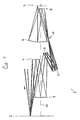
- a typical structure of an EUV projection lens 1 is shown by way of a preferred embodiment in FIG. It serves to image a pattern of a reticle or the like arranged in an object plane 2 in an image plane 3 oriented parallel to the object plane on a reduced scale, for example in the ratio 4: 1.
- the imaging takes place by means of electromagnetic radiation from the extreme ultraviolet range (EUV), in particular at a working wavelength of about 13.4 ⁇ m.
- EUV extreme ultraviolet range
- a total of six mirrors 4 to 9 provided with curved mirror surfaces and thus imaging are arranged coaxially with respect to one another, that they define a common optical axis 10 which is perpendicular to the image plane and the object plane.
- the mirror substrates 4 to 9 have the shape of rotationally symmetric aspheres whose symmetry axis coincides with the common mechanical axis 10.
- the light from an illumination system (not shown), which comprises a light source for soft X-ray radiation, initially strikes the reflective mask arranged in the object plane 2 from the image-facing side of the object plane 2.
- the reflected light impinges on a first mirror 4, which has an object-directed, concave mirror surface, which slightly narrows the impinging radiation onto a second mirror 5.
- the second mirror 5 has a concave mirror surface facing the first mirror 4, which reflects the radiation in the direction of a third mirror 6 as a convergent beam.
- the third mirror 6 has a convex mirror surface, which reflects the off-axis impinging radiation in the direction of a concave mirror surface of a fourth mirror 7.
- the latter is used in a mirror area far outside the optical axis and reflects the incident radiation to form a real intermediate image 11 on a fifth mirror 8 arranged in the vicinity of the image plane 3.
- This has a convex mirror surface facing away from the image plane, which reflects the incident divergent radiation reflected in the direction of a sixth mirror 9, which has a facing to the image plane 3, concave mirror surface with which the incident radiation is reflected and focused on the image plane 3.
- All reflective surfaces of the mirrors 4 to 9 are coated with reflection-enhancing reflective coatings.
- Preferred embodiments are layer stacks of, for example, about forty Alternating layer pairs, wherein a pair of alternating layers each comprise a silicon layer and a molybdenum layer.
- Table 1 summarizes the specification of the illustrated design in tabular form.
- Line 1 indicates the number or designation of the reflective or otherwise marked surfaces
- line 2 the radius of the surfaces (in millimeters)
- line 3 the distance of the respective surface to the following surface (in millimeters).
- the signs of the radii are chosen such that a positive sign corresponds to a curvature center of the mirror surface lying on the side of the image plane.
- Lines 4 to 9 labeled A to E indicate the aspheric coefficients of the aspheric mirror surfaces. It can be seen that all the mirror surfaces are aspherically curved.
- any layer design used may interfere with the passing wavefront only insofar as the overall system does not move out of a local minimum of its properties found in developing the basic design with uncoated substrates.
- wavefront errors of higher order hardly occur, the essential effects are distortion and defocusing.
- Quality criteria for such layer designs are, in addition to the wavefront (for example described by Zernike coefficients) and the distortion (in the scan direction corresponding to the y direction) and in the cross-scan direction (corresponding to the x direction) the field uniformity and the pupil apodization. Design and manufacturing system properties remain virtually unchanged compared to the basic design with uncoated substrates.
- a projection lens in which all reflective coatings have a constant layer thickness.
- an average value for the average angle of incidence on the respective mirror is expediently calculated from the angular load calculations for each mirror, for which purpose the average angle of incidence over the entire useful range of the mirror is averaged.
- an associated optimal layer thickness is then determined and a corresponding layer design is created in a manner known per se.
- the essential effect of the uniformly thick layers is a constant image offset in the scan direction with a clear defocusing. These first order errors can be achieved through re-optimization be corrected again.
- the wavefront aberration characterized by the rms value, resulted in a deterioration of about 20% compared to uncoated designs.
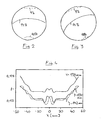
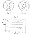
- FIG. 2 shows this distribution for a field point lying on the symmetry axis of the system
- FIG. 3 showing the distribution for a field point at the edge of the field Ringfeldes represents.
- the given percentages indicate fractions of the light intensity present at the entrance of the projection objective.
- the two intensity distributions only differ by a rotation about the axis of the exit pupil. The angle of rotation results from the position of the field point in the object or image plane.
- the schematic shows that a strong pupil apodization occurs.
- the intensity varies between about 3% and 14% across the pupil.
- the ranges of different values for the pupil intensity are shown by lines of equal intensity in FIGS. 2 and 3.
- the particular form of distribution with an out-of-exit pupil center would cause a large difference between the critical dimensions (CD's) for horizontal and vertical structures (hv difference).
- Fig. 4 shows schematically the transmission distribution across the field. While the variation in the scan direction (corresponding to the y values of the diagram) has no significant negative influence due to the integrating effect of the scanning process, the nonuniformity is perpendicular to the scan direction, ie in the cross-scan direction or x-direction , responsible for CD variations across the field.
- the near-field fifth mirror 8 is the mirror on which the largest variation of the mean angle of incidence occurs over the used mirror surface.
- the angle of incidence is the angle between the direction of incidence of the incoming radiation and the surface normal of the reflecting surface at the point of impact of the radiation.
- the incidence angle values in the example are between approx. 1 ° and 17 °. If this mirror is provided with layers of constant thickness, this leads to a relatively high loss of reflectivity.
- a favorable compromise between high reflectivity and acceptable wavefront correction is possible in that at least this mirror 8 is covered with a graded, rotationally symmetrical reflection coating whose layer thickness profile according to equation (1) can be described.
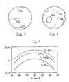
- FIGS. 5 and 6 of the intensity distributions in the exit pupil schematically show a high average transmission of, for example, 13.7%, whose fluctuation range is between approximately 12% and approximately 14%. is significantly lower than in the layer system of constant thickness described above.
- the field uniformity shown schematically in FIG. 7 is slightly worse at about 2.5% than at constant layer thicknesses.
- such layer systems with a lateral course are only suitable in exceptional cases because of a relatively strong distortion in the cross-scan direction (x-direction) because no compensation effect by the scanning process is effective for this distortion.
- this distortion in the cross-scan direction is based essentially on the decentration of the graded reflection layer of the fifth mirror 8. Accordingly, this effect can be reduced if the decentering is kept small or the graded reflection layer is arranged rotationally symmetric to the optical axis.
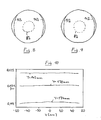
- Typical optical properties of a centered graded reflective layer design on the fifth mirror are shown in FIGS. 8-10. It can be seen that the pupil apodization is relatively large with about 8% in the area of the axis and about 14% in the edge of the pupil. However, it is rotationally symmetric to the pupil axis and thus independent of the field point. From this, the almost perfect uniformity ( ⁇ 0.4%) across the field, shown in FIG. 10, results directly. The total transmission is about 12% lower compared to the present design.
- FIGS. 11 to 13 is optimized with regard to rotationally symmetrical pupil apodization.
- centered, graded reflective coatings are applied to two mirrors, namely on the fifth mirror 8, on which the largest angle of incidence occurs, and on the third mirror 6 arranged in front of the light path.
- the centered layer courses of these mirrors are matched to one another the pupil apodization, similar to the embodiment of FIG. 8 to 10, is substantially rotationally symmetrical.
- the pupil apodization has a lower absolute value variation across the exit pupil, wherein the uniformity of the illumination is significantly better than with only one centered, graded reflective coating.
- the intensity variation in the exit pupil lies only between approximately 13.4% and approximately 15.6%, ie it is significantly lower than the corresponding variation in an embodiment with only one centered one Graded reflective coating ( Figures 8 to 10).
- the total transmission with approximately 14.7% compared to this embodiment is significantly larger and the field uniformity with values ⁇ 0.4% is almost perfect (FIG. 13).
- the rotationally symmetrical exit pupil is achieved by a specific coordination of the layer thickness profiles at the third and fifth mirror.
- the example shows that pupil homogeneity with a substantially rotationally symmetric profile can be achieved by means of a plurality of centered, graded reflective coatings whose layer thickness profiles are suitably matched to one another.
- FIGS. 14 to 16 A variant will now be described with reference to FIGS. 14 to 16, which enables an advantageous compromise between total transmission and field uniformity.
- it is preferably provided to decenter the layer profiles of a plurality, ie of at least two mirrors and to coordinate the individual decentrations so that the distortion contributions are partially or completely compensate.
- FIGS. 14 to 16 show the characteristics of a design in which, in addition to the fifth mirror 8, the third mirror 6 also has a decentered, graded reflective coating.
- the system exhibits a very high total transmission of approximately 13.6% and that shown in FIG. 16 schematically illustrated field uniformity is acceptable with about 1.6% static field uniformity.
- the value integrated by the scan movement should be in the range of 1% or less and thus be much cheaper. It can be seen in FIGS. 14 and 15 that a course of the intensity distribution in the pupil is produced by these coatings, which is somewhat less favorable than with a centered, graded coating (FIGS. 8 and 9).
- the fluctuation range is between approx. 9% and 14%.
- the apodization is not complete or rotationally symmetric, which may adversely affect telecentricity and process windows.
Landscapes
- Physics & Mathematics (AREA)
- General Physics & Mathematics (AREA)
- Optics & Photonics (AREA)
- Health & Medical Sciences (AREA)
- Engineering & Computer Science (AREA)
- Environmental & Geological Engineering (AREA)
- Epidemiology (AREA)
- Public Health (AREA)
- Lenses (AREA)
- Exposure Of Semiconductors, Excluding Electron Or Ion Beam Exposure (AREA)
- Exposure And Positioning Against Photoresist Photosensitive Materials (AREA)
- Optical Elements Other Than Lenses (AREA)
Claims (12)
- Objectif de projection destiné à représenter dans un plan d'image un modèle disposé dans un plan d'objet à l'aide d'un rayonnement électromagnétique de la plage ultraviolette extrême (EUV), plusieurs miroirs de représentation munis de revêtements réfléchissants étant disposés entre le plan d'objet et le plan d'image, lesquels définissent un axe optique de l'objectif de projection, au moins l'un des miroirs présentant un revêtement réfléchissant gradué avec un tracé d'épaisseur de couche à symétrie rotationnelle par rapport à un axe de revêtement, caractérisé en ce que le revêtement réfléchissant gradué est un revêtement réfléchissant gradué décentré, l'axe du revêtement étant disposé de manière excentrique par rapport à l'axe optique de l'objectif de projection.
- Objectif de projection selon la revendication 1, avec lequel les miroirs sont configurés et disposés les uns par rapport aux autres de telle sorte que chaque miroir peut être exposé aux rayons à partir d'une plage d'angles d'incidence caractéristique pour le miroir, au moins le miroir ayant la plage d'angles d'incidence la plus grande présentant un revêtement réfléchissant gradué décentré, l'angle d'incidence du miroir ayant la plage d'angles d'incidence la plus grande se trouvant de préférence dans une plage entre moins de 5° et plus de 10°.
- Objectif de projection selon la revendication 1 ou 2, avec lequel l'un des miroirs présente un premier revêtement réfléchissant gradué décentré et au moins l'un des autres miroirs présente un deuxième revêtement réfléchissant gradué décentré, le premier et le deuxième revêtements réfléchissants gradués décentrés étant accordés l'un sur l'autre de telle sorte que les contributions des revêtements réfléchissants aux aberrations d'image, notamment à la distorsion d'image, sont au moins partiellement compensées, les revêtements réfléchissants gradués décentrés étant de préférence disposés l'un par rapport à l'autre de telle sorte que les contributions des revêtements réfléchissants à la distorsion d'image dans une direction de balayage transversale qui s'étend perpendiculairement à une direction de balayage sont compensées.
- Objectif de projection selon l'une des revendications précédentes, avec lequel sont définies une direction de balayage et une direction de balayage dirigée perpendiculairement à celle-ci et avec lequel au moins un revêtement réfléchissant gradué décentré est décentré dans la direction du balayage.
- Objectif de projection selon l'une des revendications précédentes, avec lequel plus de cinq miroirs, notamment six miroirs sont prévus entre le plan d'objet et le plan d'image.
- Objectif de projection selon l'une des revendications précédentes, avec lequel tous les miroirs sont disposés de manière coaxiale les uns par rapport aux autres.
- Objectif de projection selon l'une des revendications précédentes, avec lequel au moins le cinquième miroir suivant le plan d'objet présente un revêtement réfléchissant gradué décentré, de préférence le quatrième et le cinquième miroir suivant le plan d'objet ou le troisième et le cinquième miroir suivant le plan d'objet présentant un revêtement réfléchissant gradué décentré.
- Objectif de projection selon l'une des revendications précédentes, avec lequel le revêtement réfléchissant gradué décentré possède un tracé d'épaisseur de couche à symétrie rotationnelle de l'épaisseur de couche (d) qui peut être décrit comme suit :

où d0 est une épaisseur de couche optimisée pour l'incidence perpendiculaire des rayons, r0 un décentrage, r une coordonnée radiale dans un plan x-y et c un coefficient. - Objectif de projection selon l'une des revendications précédentes, avec lequel l'objectif de projection possède une ouverture numérique côté image NA ≥ 0,15, notamment NA ≥ 0,2.
- Objectif de projection selon l'une des revendications précédentes, avec lequel les miroirs sont configurés et disposés de telle sorte qu'une image intermédiaire est générée entre le plan d'objet et le plan d'image.
- Objectif de projection selon l'une des revendications 1 ou 3 à 10, les miroirs étant configurés et disposés les uns par rapport aux autres de telle sorte que chaque miroir peut être exposé aux rayons à partir d'une plage d'angles d'incidence caractéristique pour le miroir, au moins le miroir ayant la plage d'angles d'incidence la plus grande présentant un revêtement réfléchissant gradué avec un tracé d'épaisseur de couche à symétrie rotationnelle par rapport à un axe de revêtement et l'axe de revêtement coïncidant pour l'essentiel avec l'axe optique de l'objectif de projection.
- Objectif de projection selon la revendication 11, avec lequel le tracé d'épaisseur de couche du revêtement réfléchissant gradué étant optimisé pour produire une homogénéité de pupille essentiellement à symétrie rotationnelle, de préférence plusieurs, de préférence un maximum de quatre miroirs munis de revêtements réfléchissants gradués centrés étant prévus, les tracés d'épaisseur de couche des revêtements réfléchissants étant accordés les uns sur les autres de telle sorte qu'une homogénéité de pupille essentiellement à symétrie rotationnelle est obtenue.
Applications Claiming Priority (2)
| Application Number | Priority Date | Filing Date | Title |
|---|---|---|---|
| US30886101P | 2001-08-01 | 2001-08-01 | |
| US308861P | 2010-02-26 |
Publications (3)
| Publication Number | Publication Date |
|---|---|
| EP1282011A2 EP1282011A2 (fr) | 2003-02-05 |
| EP1282011A3 EP1282011A3 (fr) | 2004-08-25 |
| EP1282011B1 true EP1282011B1 (fr) | 2006-11-22 |
Family
ID=23195690
Family Applications (1)
| Application Number | Title | Priority Date | Filing Date |
|---|---|---|---|
| EP02016693A Expired - Lifetime EP1282011B1 (fr) | 2001-08-01 | 2002-07-26 | Lentille de projection réflective pour la photolithographie dans l'ultraviolet extrême |
Country Status (5)
| Country | Link |
|---|---|
| US (3) | US6927901B2 (fr) |
| EP (1) | EP1282011B1 (fr) |
| JP (2) | JP4178862B2 (fr) |
| DE (1) | DE50208750D1 (fr) |
| TW (1) | TW565706B (fr) |
Cited By (2)
| Publication number | Priority date | Publication date | Assignee | Title |
|---|---|---|---|---|
| DE102016212373A1 (de) | 2016-07-07 | 2018-01-11 | Carl Zeiss Smt Gmbh | Optisches System, insbesondere für eine mikrolithographische Projektionsbelichtungsanlage |
| DE102025111510A1 (de) | 2025-03-25 | 2026-05-13 | Carl Zeiss Smt Gmbh | Verfahren zum Optimieren einer abbildenden DUV/UV-Optik für eine Projektionsbelichtungsanlage |
Families Citing this family (54)
| Publication number | Priority date | Publication date | Assignee | Title |
|---|---|---|---|---|
| US7843632B2 (en) * | 2006-08-16 | 2010-11-30 | Cymer, Inc. | EUV optics |
| US7053988B2 (en) * | 2001-05-22 | 2006-05-30 | Carl Zeiss Smt Ag. | Optically polarizing retardation arrangement, and microlithography projection exposure machine |
| JP2004325649A (ja) * | 2003-04-23 | 2004-11-18 | Canon Inc | 反射型投影光学系、露光装置及びデバイスの製造方法 |
| DE10329793A1 (de) * | 2003-07-01 | 2005-01-27 | Carl Zeiss Smt Ag | Projektionsobjektiv für eine mikrolithographische Projektionsbelichtungsanlage |
| EP1496521A1 (fr) | 2003-07-09 | 2005-01-12 | ASML Netherlands B.V. | Miroir et appareil lithographique avec miroir |
| KR100983190B1 (ko) | 2003-09-17 | 2010-09-20 | 칼 짜이스 에스엠테 아게 | 마스크, 리소그래피 장치와 반도체 구성요소 |
| US7164535B2 (en) * | 2003-09-30 | 2007-01-16 | Teledyne Licensing, Llc | Optical coating and configuration for tailored spectral characteristics over viewing angle |
| US7081956B1 (en) | 2003-12-04 | 2006-07-25 | Advanced Micro Devices, Inc. | Method and device for determining reflection lens pupil transmission distribution and illumination intensity distribution in reflective imaging system |
| US6977717B1 (en) * | 2003-12-04 | 2005-12-20 | Advanced Micro Devices, Inc. | Method and device for determining projection lens pupil transmission distribution and illumination intensity distribution in photolithographic imaging system |
| JP2005172988A (ja) * | 2003-12-09 | 2005-06-30 | Nikon Corp | 投影光学系および該投影光学系を備えた露光装置 |
| US7522335B2 (en) * | 2004-03-29 | 2009-04-21 | Intel Corporation | Broad-angle multilayer mirror design |
| JP4532991B2 (ja) | 2004-05-26 | 2010-08-25 | キヤノン株式会社 | 投影光学系、露光装置及びデバイス製造方法 |
| KR101248328B1 (ko) * | 2004-06-04 | 2013-04-01 | 칼 짜이스 에스엠티 게엠베하 | 강도 변동이 보상된 투사 시스템 및 이를 위한 보상 요소 |
| JP4498059B2 (ja) * | 2004-08-17 | 2010-07-07 | キヤノン株式会社 | 光学素子、露光装置及び成膜方法 |
| JP4498060B2 (ja) * | 2004-08-18 | 2010-07-07 | キヤノン株式会社 | 投影光学系、露光装置及び光学素子の製造方法 |
| DE102005042496A1 (de) * | 2005-09-05 | 2007-03-08 | Carl Zeiss Sms Gmbh | Verfahren zur Korrektur der Apodisierung in mikroskopischen Abbildungssystemen |
| US7773196B2 (en) * | 2006-03-10 | 2010-08-10 | Nikon Corporation | Projection-optical systems and exposure apparatus comprising same |
| US20080118849A1 (en) * | 2006-11-21 | 2008-05-22 | Manish Chandhok | Reflective optical system for a photolithography scanner field projector |
| EP1930771A1 (fr) * | 2006-12-04 | 2008-06-11 | Carl Zeiss SMT AG | Objectif de projection possédant des éléments de miroir avec des revêtements réfléchissants |
| JP5269079B2 (ja) * | 2007-08-20 | 2013-08-21 | カール・ツァイス・エスエムティー・ゲーエムベーハー | 反射コーティングを備えたミラー要素を有する投影対物系 |
| DE102007051669A1 (de) * | 2007-10-26 | 2009-04-30 | Carl Zeiss Smt Ag | Abbildende Optik, Projektionsbelichtungsanlage für die Mikrolithographie mit einer derartigen abbildenden Optik sowie Verfahren zur Herstellung eines mikrostrukturierten Bauteils mit einer derartigen Projektionsbelichtungsanlage |
| DE102007062198A1 (de) * | 2007-12-21 | 2009-06-25 | Carl Zeiss Microimaging Gmbh | Katoptrisches Objektiv zur Abbildung eines im Wesentlichen linienförmigen Objektes |
| JP2010199503A (ja) * | 2009-02-27 | 2010-09-09 | Nikon Corp | 光学素子、露光装置及びデバイス製造方法 |
| EP2414884A1 (fr) * | 2009-03-30 | 2012-02-08 | Carl Zeiss SMT GmbH | Optique d'imagerie et installation d'exposition de projection pour microlithographie comportant une optique d'imagerie de ce type |
| US8050380B2 (en) * | 2009-05-05 | 2011-11-01 | Media Lario, S.R.L. | Zone-optimized mirrors and optical systems using same |
| JP5070242B2 (ja) * | 2009-05-27 | 2012-11-07 | カール・ツァイス・エスエムティー・ゲーエムベーハー | リソグラフィ装置 |
| DE102009047179B8 (de) | 2009-11-26 | 2016-08-18 | Carl Zeiss Smt Gmbh | Projektionsobjektiv |
| DE102011003145A1 (de) | 2010-02-09 | 2011-08-11 | Carl Zeiss SMT GmbH, 73447 | Optisches System mit Blendeneinrichtung |
| DE102011005144A1 (de) * | 2010-03-17 | 2011-09-22 | Carl Zeiss Smt Gmbh | Reflektives optisches Element, Projektionssystem und Projektionsbelichtungsanlage |
| US8023183B1 (en) * | 2010-04-23 | 2011-09-20 | Raytheon Company | All-reflective wide-field-of-view telescope with beneficial distortion correction |
| US8317344B2 (en) | 2010-06-08 | 2012-11-27 | Nikon Corporation | High NA annular field catoptric projection optics using Zernike polynomial mirror surfaces |
| CN102444790B (zh) * | 2010-09-30 | 2014-11-19 | 光宝电子(广州)有限公司 | 灯具 |
| DE102010062597A1 (de) * | 2010-12-08 | 2012-06-14 | Carl Zeiss Smt Gmbh | Reflektives optisches Abbildungssystem |
| DE102011075579A1 (de) * | 2011-05-10 | 2012-11-15 | Carl Zeiss Smt Gmbh | Spiegel und Projektionsbelichtungsanlage für die Mikrolithographie mit einem solchen Spiegel |
| DE102012202057B4 (de) * | 2012-02-10 | 2021-07-08 | Carl Zeiss Smt Gmbh | Projektionsobjektiv für EUV-Mikrolithographie, Folienelement und Verfahren zur Herstellung eines Projektionsobjektivs mit Folienelement |
| DE102012202536A1 (de) | 2012-02-20 | 2013-08-22 | Carl Zeiss Smt Gmbh | Projektionsbelichtungsverfahren und Projektionsbelichtungsanlage für die Mikrolithographie |
| CN102681357B (zh) * | 2012-04-01 | 2014-02-05 | 北京理工大学 | 一种极紫外光刻投影物镜设计方法 |
| DE102012205615A1 (de) | 2012-04-04 | 2013-10-10 | Carl Zeiss Smt Gmbh | Beschichtungsverfahren, Beschichtungsanlage und optisches Element mit Beschichtung |
| DE102013203364A1 (de) * | 2013-02-28 | 2014-09-11 | Carl Zeiss Smt Gmbh | Reflektierende Beschichtung mit optimierter Dicke |
| JP5746259B2 (ja) * | 2013-05-07 | 2015-07-08 | カール・ツァイス・エスエムティー・ゲーエムベーハー | 反射コーティングを備えたミラー要素を有する投影対物系 |
| US9316808B1 (en) | 2014-03-16 | 2016-04-19 | Hyperion Development, LLC | Optical assembly for a wide field of view point action camera with a low sag aspheric lens element |
| US9494772B1 (en) | 2014-03-16 | 2016-11-15 | Hyperion Development, LLC | Optical assembly for a wide field of view point action camera with low field curvature |
| US9726859B1 (en) | 2014-03-16 | 2017-08-08 | Navitar Industries, Llc | Optical assembly for a wide field of view camera with low TV distortion |
| US9995910B1 (en) | 2014-03-16 | 2018-06-12 | Navitar Industries, Llc | Optical assembly for a compact wide field of view digital camera with high MTF |
| US10139595B1 (en) | 2014-03-16 | 2018-11-27 | Navitar Industries, Llc | Optical assembly for a compact wide field of view digital camera with low first lens diameter to image diagonal ratio |
| US9316820B1 (en) | 2014-03-16 | 2016-04-19 | Hyperion Development, LLC | Optical assembly for a wide field of view point action camera with low astigmatism |
| US10545314B1 (en) | 2014-03-16 | 2020-01-28 | Navitar Industries, Llc | Optical assembly for a compact wide field of view digital camera with low lateral chromatic aberration |
| US9091843B1 (en) | 2014-03-16 | 2015-07-28 | Hyperion Development, LLC | Optical assembly for a wide field of view point action camera with low track length to focal length ratio |
| US10386604B1 (en) | 2014-03-16 | 2019-08-20 | Navitar Industries, Llc | Compact wide field of view digital camera with stray light impact suppression |
| US9835835B1 (en) | 2015-04-10 | 2017-12-05 | Navitar Industries, Llc | Projection zoom lens and camera |
| DE102016117851A1 (de) * | 2016-09-22 | 2018-03-22 | Valeo Schalter Und Sensoren Gmbh | Sendeeinrichtung für eine optische Erfassungsvorrichtung, optische Erfassungsvorrichtung, Kraftfahrzeug sowie Verfahren |
| DE102017202802A1 (de) * | 2017-02-21 | 2018-08-23 | Carl Zeiss Smt Gmbh | Objektiv und optisches System mit einem solchen Objektiv |
| LU100753B1 (de) | 2018-03-28 | 2019-10-01 | Highyag Lasertechnologie Gmbh | Zoomoptik |
| DE102023120807A1 (de) | 2023-08-04 | 2025-02-06 | Asml Netherlands B.V. | Verfahren und System zur Bestimmung feldabhängiger Aberrationen |
Family Cites Families (17)
| Publication number | Priority date | Publication date | Assignee | Title |
|---|---|---|---|---|
| US4804258A (en) * | 1986-05-05 | 1989-02-14 | Hughes Aircraft Company | Four mirror afocal wide field of view optical system |
| EP0252734B1 (fr) * | 1986-07-11 | 2000-05-03 | Canon Kabushiki Kaisha | Système d'exposition, par projection en réduction, de rayons X, du type réflectif |
| US5063586A (en) * | 1989-10-13 | 1991-11-05 | At&T Bell Laboratories | Apparatus for semiconductor lithography |
| US5315629A (en) * | 1990-10-10 | 1994-05-24 | At&T Bell Laboratories | Ringfield lithography |
| US5222112A (en) * | 1990-12-27 | 1993-06-22 | Hitachi, Ltd. | X-ray pattern masking by a reflective reduction projection optical system |
| EP0566001B1 (fr) * | 1992-04-07 | 1999-07-14 | Raytheon Company | Système optique d'affichage d'image virtuelle à large bande spectrale |
| EP0927857B1 (fr) * | 1992-11-25 | 2003-09-03 | Solar Systems Pty Ltd | Dispositif séparant le rayonnement solaire en composantes de longue et courte longueur d'onde |
| US5825553A (en) * | 1993-11-29 | 1998-10-20 | Hughes Aircraft Company Now Known As Ragtheon Company | Eyepiece design |
| US5815310A (en) | 1995-12-12 | 1998-09-29 | Svg Lithography Systems, Inc. | High numerical aperture ring field optical reduction system |
| JPH09326347A (ja) | 1996-06-05 | 1997-12-16 | Hitachi Ltd | 微細パターン転写方法およびその装置 |
| US5911858A (en) * | 1997-02-18 | 1999-06-15 | Sandia Corporation | Method for high-precision multi-layered thin film deposition for deep and extreme ultraviolet mirrors |
| US5973826A (en) * | 1998-02-20 | 1999-10-26 | Regents Of The University Of California | Reflective optical imaging system with balanced distortion |
| US6072852A (en) * | 1998-06-09 | 2000-06-06 | The Regents Of The University Of California | High numerical aperture projection system for extreme ultraviolet projection lithography |
| US6600552B2 (en) * | 1999-02-15 | 2003-07-29 | Carl-Zeiss Smt Ag | Microlithography reduction objective and projection exposure apparatus |
| EP1772775B1 (fr) * | 1999-02-15 | 2008-11-05 | Carl Zeiss SMT AG | Dispositif à objectif de réduction pour la microlithographique ainsi qu'une installation d'éclairage à projection |
| US6188513B1 (en) * | 1999-03-15 | 2001-02-13 | Russell Hudyma | High numerical aperture ring field projection system for extreme ultraviolet lithography |
| US6033079A (en) * | 1999-03-15 | 2000-03-07 | Hudyma; Russell | High numerical aperture ring field projection system for extreme ultraviolet lithography |
-
2002
- 2002-07-26 EP EP02016693A patent/EP1282011B1/fr not_active Expired - Lifetime
- 2002-07-26 DE DE50208750T patent/DE50208750D1/de not_active Expired - Lifetime
- 2002-07-26 JP JP2002218003A patent/JP4178862B2/ja not_active Expired - Fee Related
- 2002-08-01 US US10/208,842 patent/US6927901B2/en not_active Expired - Lifetime
- 2002-08-01 TW TW091117312A patent/TW565706B/zh not_active IP Right Cessation
-
2005
- 2005-07-19 US US11/183,877 patent/US7199922B2/en not_active Expired - Lifetime
-
2007
- 2007-03-22 US US11/723,831 patent/US7450301B2/en not_active Expired - Fee Related
-
2008
- 2008-07-10 JP JP2008180036A patent/JP2008262223A/ja active Pending
Cited By (4)
| Publication number | Priority date | Publication date | Assignee | Title |
|---|---|---|---|---|
| DE102016212373A1 (de) | 2016-07-07 | 2018-01-11 | Carl Zeiss Smt Gmbh | Optisches System, insbesondere für eine mikrolithographische Projektionsbelichtungsanlage |
| WO2018007081A1 (fr) | 2016-07-07 | 2018-01-11 | Carl Zeiss Smt Gmbh | Système optique, destiné en particulier à un appareil d'exposition par projection microlithographique |
| US10520827B2 (en) | 2016-07-07 | 2019-12-31 | Carl Zeiss Smt Gmbh | Optical system, in particular for a microlithographic projection exposure apparatus |
| DE102025111510A1 (de) | 2025-03-25 | 2026-05-13 | Carl Zeiss Smt Gmbh | Verfahren zum Optimieren einer abbildenden DUV/UV-Optik für eine Projektionsbelichtungsanlage |
Also Published As
| Publication number | Publication date |
|---|---|
| US7450301B2 (en) | 2008-11-11 |
| TW565706B (en) | 2003-12-11 |
| DE50208750D1 (de) | 2007-01-04 |
| EP1282011A2 (fr) | 2003-02-05 |
| US20050248835A1 (en) | 2005-11-10 |
| US20070171558A1 (en) | 2007-07-26 |
| JP2003177319A (ja) | 2003-06-27 |
| US6927901B2 (en) | 2005-08-09 |
| US20030099034A1 (en) | 2003-05-29 |
| JP2008262223A (ja) | 2008-10-30 |
| EP1282011A3 (fr) | 2004-08-25 |
| US7199922B2 (en) | 2007-04-03 |
| JP4178862B2 (ja) | 2008-11-12 |
Similar Documents
| Publication | Publication Date | Title |
|---|---|---|
| EP1282011A2 (fr) | Lentille de projection réflective pour la photolithographie dans l'ultraviolet extrême | |
| EP1772775B1 (fr) | Dispositif à objectif de réduction pour la microlithographique ainsi qu'une installation d'éclairage à projection | |
| DE69122018T2 (de) | Röntgenstrahllithographie mit ringförmigem Bildfeld | |
| DE102012202057B4 (de) | Projektionsobjektiv für EUV-Mikrolithographie, Folienelement und Verfahren zur Herstellung eines Projektionsobjektivs mit Folienelement | |
| DE102015226531A1 (de) | Abbildende Optik zur Abbildung eines Objektfeldes in ein Bildfeld sowie Projektionsbelichtungsanlage mit einer derartigen abbildenden Optik | |
| DE102014208770A1 (de) | Projektionsoptik zur Abbildung eines Objektfeldes in ein Bildfeld sowie Projektionsbelichtungsanlage mit einer derartigen Projektionsoptik | |
| DE10052289A1 (de) | 8-Spiegel-Mikrolithographie-Projektionsobjektiv | |
| EP1845417B1 (fr) | Système d'éclairage doté d'un objectif à zoom | |
| DE102016218996A1 (de) | Abbildende Optik für die Projektionslithographie | |
| EP1327172A1 (fr) | Objectif de projection par microlithographie a 8 miroirs | |
| EP1950594A1 (fr) | Système optique, installation d'éclairage à projection pour la microlithographie dotée d'une telle système optique, procédé de fabrication d'un composant microstructuré à l'aide d'une telle installation d'éclairage à projection, composant microstructuré fabriqué selon ce procédé de fabrication, ainsi qu'utilisation d'une telle système optique | |
| DE102010040811A1 (de) | Abbildende Optik | |
| EP1260845A2 (fr) | Objectif de réduction catadioptrique | |
| EP1480082A1 (fr) | Système de quatre miroirs à champ annulaire pour lithographie EUV | |
| DE102008043162A1 (de) | Abbildende Optik sowie Projektionsbelichtungsanlage für die Mikrolithographie mit einer derartigen abbildenden Optik | |
| DE102008042917A1 (de) | Abbildende Optik sowie Projektionsbelichtungsanlage für die Mikrolithographie mit einer derartigen abbildenden Optik | |
| DE102014218474A1 (de) | Projektionsobjektiv, Projektionsbelichtungsanlage und Projektionsbelichtungsverfahren für die EUV-Mikrolithographie | |
| DE102008033341A1 (de) | Projektionsobjektiv | |
| DE102007051671A1 (de) | Abbildende Optik sowie Projektionsbelichtungsanlage für die Mikrolithographie mit einer derartigen abbildenden Optik | |
| DE102015212619A1 (de) | Abbildende Optik zur Abbildung eines Objektfeldes in ein Bildfeld sowie Projektionsbelichtungsanlage mit einer derartigen abbildenden Optik | |
| DE102015221984A1 (de) | Abbildende Optik zur Abbildung eines Objektfeldes in ein Bildfeld sowie Projektionsbelichtungsanlage mit einer derartigen abbildenden Optik | |
| DE102018214437A1 (de) | Abbildende Optik zur Abbildung eines Objektfeldes in ein Bildfeld sowie Projektionsbelichtungsanlage mit einer derartigen abbildenden Optik | |
| DE102006043251A1 (de) | Mikrolithographie-Projektionsobjektiv, Projektionsbelichtungsanlage mit einem derartigen Objektiv, Herstellungsverfahren mikrostrukturierter Bauteile mit einer derartigen Projektionsbelichtungsanlage sowie mit diesem Verfahren hergestelltes Bauteil | |
| EP1037115B1 (fr) | Objectif de projection microlithographique et appareil d' exposition par projection | |
| WO2018104178A1 (fr) | Objectif de projection catadioptrique et son procédé de fabrication |
Legal Events
| Date | Code | Title | Description |
|---|---|---|---|
| PUAI | Public reference made under article 153(3) epc to a published international application that has entered the european phase |
Free format text: ORIGINAL CODE: 0009012 |
|
| AK | Designated contracting states |
Designated state(s): AT BE BG CH CY CZ DE DK EE ES FI FR GB GR IE IT LI LU MC NL PT SE SK TR |
|
| AX | Request for extension of the european patent |
Extension state: AL LT LV MK RO SI |
|
| PUAL | Search report despatched |
Free format text: ORIGINAL CODE: 0009013 |
|
| AK | Designated contracting states |
Kind code of ref document: A3 Designated state(s): AT BE BG CH CY CZ DE DK EE ES FI FR GB GR IE IT LI LU MC NL PT SE SK TR |
|
| AX | Request for extension of the european patent |
Extension state: AL LT LV MK RO SI |
|
| RAP1 | Party data changed (applicant data changed or rights of an application transferred) |
Owner name: CARL ZEISS SMT AG |
|
| 17P | Request for examination filed |
Effective date: 20050120 |
|
| AKX | Designation fees paid |
Designated state(s): DE FR GB NL |
|
| 17Q | First examination report despatched |
Effective date: 20050502 |
|
| GRAP | Despatch of communication of intention to grant a patent |
Free format text: ORIGINAL CODE: EPIDOSNIGR1 |
|
| GRAS | Grant fee paid |
Free format text: ORIGINAL CODE: EPIDOSNIGR3 |
|
| GRAA | (expected) grant |
Free format text: ORIGINAL CODE: 0009210 |
|
| AK | Designated contracting states |
Kind code of ref document: B1 Designated state(s): DE FR GB NL |
|
| REG | Reference to a national code |
Ref country code: GB Ref legal event code: FG4D Free format text: NOT ENGLISH |
|
| REF | Corresponds to: |
Ref document number: 50208750 Country of ref document: DE Date of ref document: 20070104 Kind code of ref document: P |
|
| GBT | Gb: translation of ep patent filed (gb section 77(6)(a)/1977) |
Effective date: 20070205 |
|
| ET | Fr: translation filed | ||
| RAP2 | Party data changed (patent owner data changed or rights of a patent transferred) |
Owner name: CARL ZEISS SMT AG |
|
| PLBE | No opposition filed within time limit |
Free format text: ORIGINAL CODE: 0009261 |
|
| STAA | Information on the status of an ep patent application or granted ep patent |
Free format text: STATUS: NO OPPOSITION FILED WITHIN TIME LIMIT |
|
| 26N | No opposition filed |
Effective date: 20070823 |
|
| NLT2 | Nl: modifications (of names), taken from the european patent patent bulletin |
Owner name: CARL ZEISS SMT AG Effective date: 20070905 |
|
| REG | Reference to a national code |
Ref country code: FR Ref legal event code: PLFP Year of fee payment: 14 |
|
| PGFP | Annual fee paid to national office [announced via postgrant information from national office to epo] |
Ref country code: FR Payment date: 20150626 Year of fee payment: 14 |
|
| PGFP | Annual fee paid to national office [announced via postgrant information from national office to epo] |
Ref country code: NL Payment date: 20150721 Year of fee payment: 14 |
|
| PGFP | Annual fee paid to national office [announced via postgrant information from national office to epo] |
Ref country code: GB Payment date: 20150721 Year of fee payment: 14 Ref country code: DE Payment date: 20150721 Year of fee payment: 14 |
|
| REG | Reference to a national code |
Ref country code: DE Ref legal event code: R119 Ref document number: 50208750 Country of ref document: DE |
|
| REG | Reference to a national code |
Ref country code: NL Ref legal event code: MM Effective date: 20160801 |
|
| GBPC | Gb: european patent ceased through non-payment of renewal fee |
Effective date: 20160726 |
|
| PG25 | Lapsed in a contracting state [announced via postgrant information from national office to epo] |
Ref country code: NL Free format text: LAPSE BECAUSE OF NON-PAYMENT OF DUE FEES Effective date: 20160801 Ref country code: FR Free format text: LAPSE BECAUSE OF NON-PAYMENT OF DUE FEES Effective date: 20160801 Ref country code: DE Free format text: LAPSE BECAUSE OF NON-PAYMENT OF DUE FEES Effective date: 20170201 |
|
| REG | Reference to a national code |
Ref country code: FR Ref legal event code: ST Effective date: 20170331 |
|
| PG25 | Lapsed in a contracting state [announced via postgrant information from national office to epo] |
Ref country code: GB Free format text: LAPSE BECAUSE OF NON-PAYMENT OF DUE FEES Effective date: 20160726 |