EP1282211A2 - Ladung/Entladungsschutzschaltung - Google Patents
Ladung/Entladungsschutzschaltung Download PDFInfo
- Publication number
- EP1282211A2 EP1282211A2 EP02392013A EP02392013A EP1282211A2 EP 1282211 A2 EP1282211 A2 EP 1282211A2 EP 02392013 A EP02392013 A EP 02392013A EP 02392013 A EP02392013 A EP 02392013A EP 1282211 A2 EP1282211 A2 EP 1282211A2
- Authority
- EP
- European Patent Office
- Prior art keywords
- voltage
- switch
- protection circuit
- circuit
- charge
- Prior art date
- Legal status (The legal status is an assumption and is not a legal conclusion. Google has not performed a legal analysis and makes no representation as to the accuracy of the status listed.)
- Withdrawn
Links
Images


Classifications
-
- H—ELECTRICITY
- H02—GENERATION; CONVERSION OR DISTRIBUTION OF ELECTRIC POWER
- H02H—EMERGENCY PROTECTIVE CIRCUIT ARRANGEMENTS
- H02H7/00—Emergency protective circuit arrangements specially adapted for specific types of electric machines or apparatus or for sectionalised protection of cable or line systems, and effecting automatic switching in the event of an undesired change from normal working conditions
- H02H7/18—Emergency protective circuit arrangements specially adapted for specific types of electric machines or apparatus or for sectionalised protection of cable or line systems, and effecting automatic switching in the event of an undesired change from normal working conditions for batteries; for accumulators
-
- H—ELECTRICITY
- H02—GENERATION; CONVERSION OR DISTRIBUTION OF ELECTRIC POWER
- H02J—ELECTRIC POWER NETWORKS; CIRCUIT ARRANGEMENTS OR SYSTEMS FOR SUPPLYING OR DISTRIBUTING ELECTRIC POWER; SYSTEMS FOR STORING ELECTRIC ENERGY
- H02J7/00—Circuit arrangements for charging or discharging batteries or for supplying loads from batteries
- H02J7/60—Circuit arrangements for charging or discharging batteries or for supplying loads from batteries including safety or protection arrangements
- H02J7/663—Circuit arrangements for charging or discharging batteries or for supplying loads from batteries including safety or protection arrangements using battery or load disconnect circuits
-
- H—ELECTRICITY
- H02—GENERATION; CONVERSION OR DISTRIBUTION OF ELECTRIC POWER
- H02J—ELECTRIC POWER NETWORKS; CIRCUIT ARRANGEMENTS OR SYSTEMS FOR SUPPLYING OR DISTRIBUTING ELECTRIC POWER; SYSTEMS FOR STORING ELECTRIC ENERGY
- H02J7/00—Circuit arrangements for charging or discharging batteries or for supplying loads from batteries
- H02J7/60—Circuit arrangements for charging or discharging batteries or for supplying loads from batteries including safety or protection arrangements
- H02J7/64—Circuit arrangements for charging or discharging batteries or for supplying loads from batteries including safety or protection arrangements against overvoltage
Definitions
- the invention refers to a charge/discharge protection circuit for a rechargeable battery comprising at least one rechargeable cell, with a control logic which opens or closes a load current switch depending on the magnitude of the voltage at the battery terminals, the voltage at the charge/discharge terminals of the protection circuit, and the charge or discharge current.
- control logic comprises an over-voltage detector which produces a control signal when reaching a voltage limit which depends on the electric strength as determined by the protection circuit.
- This control signal closes a short-circuit switch which connects the battery terminals via a load current switch in series with a fusible link.
- Such a circuit is deemed known from the this-side DE-A-101 03 3362, which is expressly referenced herewith.
- this circuit can be disposed between a single lithium-ion cell and the electronics of a mobile phone. It can be produced at favorable cost with a significantly lower electric strength than inherently required in a worst case, because the short-circuit switch closes when reaching an appropriately determined voltage limit. The resulting short circuit current thus safely destroys the fusible link so that the cell is protected from a dangerous overcharge.
- the fusible link cannot be integrated, or only at high cost, on an IC because it has to respond very reliably at a tightly toleranced nominal current.
- the central idea of the invention is, therefore, to create the condition where the fuse segments in the case of an over-voltage are reliably destroyed and where the destruction proceeds sequentially from the first to the last fuse segment.
- This is achieved by dividing the functions of the load current switch, the fusible link, and the short-circuit switch into in parallel arranged T-sections, each of which is designed for only a fraction of the nominal load so that each of the easily integrated fuse segments carry only the respective fraction of the nominal current. It is important in this case that the entire protection circuit or its control logic will not be destroyed before through that unduly high over-voltage, in which case the sequential blowing of the fuse segments would no longer be guaranteed. This is taken care of by the semiconductor switch which immediately short-circuits a recognized over-voltage.
- the over-voltage detector receives as input voltage the voltage at the charge/discharge terminals.
- the over-voltage detector could also receive as input voltage the voltage via the parallel circuit of the opened load current switches, the load current switches having opened due to the over-current caused by the previous over-voltage.
- At least those circuit components of the control logic generating the control signals for the switch segments receive their supply voltage from an auxiliary voltage source, in particular from a charged buffer capacitor. This safeguards the function of the protection circuit when the outer over-voltage is short-circuited by the semiconductor switch or if it is so high that it has lead to a destruction of other intended parts of the control logic.
- the over-voltage detector may in particular comprise a bistable flip-flop circuit, which switches to its second stable state when the predetermined voltage limit is reached, so that the sequential closing of the switch segments of the short-circuit switch is initiated when the predetermined voltage limit is reached during even briefly.
- the over-voltage detector may comprise a clock generator followed by a shift register of at least n levels, which, when reaching the predetermined voltage limit, delivers sequentially the control signals for the switch segments of the short-circuit switch.
- each switch segment of the short-circuit switch has associated with it a voltage detector, which delivers a signal at its output when the voltage at this switch segment disappears as a result of the blowing of the associated fuse segment whereby the outputs of the voltage detectors are coupled to a logic circuit which comprises a clock generator and which, when exceeding the voltage limit, produces the control signal for the next in line switch segment only when the voltage detector of the preceding switch segment delivers an output signal.
- the logic circuit can be realized, in particular, with an appropriate number of sequentially connected and with each other coupled flip-flops, as is well understood by those skilled in the art, or an appropriate number of short shift registers.
- the semiconductor switch and/or the switch segments of the short-circuit switch may comprise two in series connected, parallel controlled single switches, in order that these components may also be realized in a low-cost technology offering only low electric strength.
- circuit components are integrated on a chip.
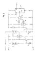
- the protection circuit illustrated in Figure 1 is located as an integrated circuit between the terminals of a Li-Ion cell 1 and two charge/discharge terminals 50 and 60, paralleled to which is a filter-capacitor 40 as protection against steeply sloped voltage increases.
- the protection circuit has the outer connections Com, +Batt and Out as well as +V H .
- the latter is connected via a buffer capacitor 2 with the reference potential Com.
- Buffer capacitor 2 is normally charged to the battery voltage via semiconductor switch 4 (indicated as a diode). If this supply voltage drops away then semiconductor switch 4 opens and the buffer capacitor 2 supplies, via line 5, power for a time for essential parts of the integrated circuit.
- a charge pump circuit may also be used in place of semiconductor switch 4, where the charge pump circuit charges the buffer capacitor 2 to the intended maximum gate voltage as dictated by the technology of the integrated circuit.
- a current sensing resistor R sense is placed between Out and +Batt in series with a circuit arrangement, which comprises a plurality of parallel coupled series circuits, in turn each comprising a load current switch 10 1 , 10 2 ,... 10 n and an integrated fusible link 11 1 , 11 2 ,... 11 n .
- a circuit arrangement which comprises a plurality of parallel coupled series circuits, in turn each comprising a load current switch 10 1 , 10 2 ,... 10 n and an integrated fusible link 11 1 , 11 2 ,... 11 n .
- Each connection node between a load current switch 10 x and a fusible link 11 x is connected to the reference potential Com via its own short-circuit switch 12 1 , 12 2 ,... 12 n .
- a control logic pictured in simplified form within dash-dotted block 6, generates by generally known means through differential amplifiers D1 and D2 a battery under-voltage signal UV and a battery over-voltage signal OV, provided the voltage of the Li-Ion cell is outside of the predetermined tolerance range.
- the control logic further generates from the voltage drop across R sense by means of differential amplifiers D3, D4 the output signals OCD, OCC, respectively, when reaching the maximum charge current or the maximum discharge current, respectively.
- Output signals UV, OV, OCC and OCD of differential amplifiers D1 to D4 are coupled into OR-gate OD which supplies an output signal F1 which opens in each of the mentioned cases all load current switches 10 1 through 10 n .
- the voltage V out is applied at the same time to the input of an over-voltage detector OVD which generates an error signal F2 in case of an over-voltage.
- Error signal F2 also closes at the same time two semiconductor switches 7, 8 which are connected in series between Com and Out, generates via OR-gate OD the error signal F1 to open the load current switches 10 1 through 10 n , and activates a clock generator CLK.
- Coupled to the clock generator CLK is a shift register SR which then sequentially delivers error signals F3 [1:n] for successive closing of the short-circuit switches 12 1 through 12 n .
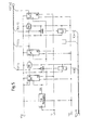
- Figure 2 illustrates an embodiment of the over-voltage detector.
- the designations of the outer connections correspond with those of Figure 1.
- Placed between Out and Com is a series circuit comprising first trigger element 21 and a resistor 22 as well as a second trigger element 23 and a second resistor 24.
- Trigger elements 21, 23 are only illustrated symbolically as the series connection of a zener diode and a back current diode wired back-to-back.
- MOS transistor T1 or T2 which in turn sets to A0" or AL@ the following Schmitt-Trigger ST1, ST2, respectively.
- the outputs of the Schmitt-Triggers are coupled via Inverter I with the inputs of a NAND-gate 25, whose output in turn is connected with the clock input of a D flip-flop 26. Its D-input is normally at A1" or AH@.
- the output Q of flip-flop 26, therefore, goes to AH@ when at the clock input an impulse arrives from OR-gate 25.
- the over-voltage detector behaves, therefore, like a bistable flip-flop.
- the output signal AH@ represents the signal F2.
- FIG. 3 illustrates clock generator CLK with the shift register SR coupled to it as shown in Figure 1.
- Clock generator CLK is started when signal F2 is applied to its start input EN and supplies at its output clock pulses clk, which are applied to the clock input of shift register SR. At the same time the latter receives at its signal input XR the signal F2 and at its D-input the signal A1" or AH@.
- Shift register SR outputs Q 1 , Q 2 , ... Q n , equal to signal F3 [1:n], thus switch sequentially from AL@ to AH@ in accordance with the clock signal, thereby delivering sequentially following control signals for closing of the switch segments 12 1 through 12 n in Figure 1.
- Figure 4 illustrates a block diagram of a second embodiment of the protection circuit. Having a similar arrangement as the embodiment of Fig. 1, it differs from that because voltages V 1 through V n-1 picked off at the short-circuit switches 12 1 through 12 n are selected and then supplied to a logic circuit LS, replacing the shift register SR of Fig. 1.
- This logic circuit LS supplies sequentially the control signals F3 [1:n] and is illustrated in Fig. 5. It receives those in Fig. 4 named voltages or signals and includes for each switch segment 12 1 through 12 n , respectively the voltages V 1 through V n-1 picked off from each, a voltage detector ST illustrated as a Schmitt-Trigger, and a number of D-flip-flops DFF 1 through DFF n whose number equals the number of switch elements.
- the clock generator CLK preferably operating at a higher frequency than the one of Fig. 1, will be started by signal F2 as before and delivers clock signals clk to the clock input of DFF 1 .
- a further improvement consists of replacing each of the flip-flops DFF by a short shift register, e.g. with three successive, appropriately coupled D-flip-flops.
- each control signal will be generated after a time delay of e.g. three clock cycles, after the voltage V x at the respective switch element has dropped, due to the blowing of the respective fuse element, below the switching threshold of the voltage detector. During this time delay the current path of the just- before blown fuse element can cool down. This method avoids having a retroactive effect on the response characteristics of the physically closely spaced adjacent, and still intact, fuse element.
Landscapes
- Engineering & Computer Science (AREA)
- Power Engineering (AREA)
- Protection Of Static Devices (AREA)
- Charge And Discharge Circuits For Batteries Or The Like (AREA)
- Emergency Protection Circuit Devices (AREA)
- Secondary Cells (AREA)
Applications Claiming Priority (2)
| Application Number | Priority Date | Filing Date | Title |
|---|---|---|---|
| DE10137875 | 2001-08-02 | ||
| DE10137875A DE10137875C1 (de) | 2001-08-02 | 2001-08-02 | Lade/Entlade-Schutzschaltung |
Publications (2)
| Publication Number | Publication Date |
|---|---|
| EP1282211A2 true EP1282211A2 (de) | 2003-02-05 |
| EP1282211A3 EP1282211A3 (de) | 2008-03-05 |
Family
ID=7694115
Family Applications (1)
| Application Number | Title | Priority Date | Filing Date |
|---|---|---|---|
| EP02392013A Withdrawn EP1282211A3 (de) | 2001-08-02 | 2002-08-02 | Ladung/Entladungsschutzschaltung |
Country Status (5)
| Country | Link |
|---|---|
| US (1) | US6687103B2 (de) |
| EP (1) | EP1282211A3 (de) |
| JP (1) | JP3927092B2 (de) |
| KR (1) | KR100981031B1 (de) |
| DE (1) | DE10137875C1 (de) |
Cited By (5)
| Publication number | Priority date | Publication date | Assignee | Title |
|---|---|---|---|---|
| EP1492211A1 (de) * | 2003-06-24 | 2004-12-29 | NEC Corporation | Verfahren und Schaltung zum Schutz eines batteriebetriebenen elektronischen Geräts |
| EP2704288A4 (de) * | 2011-04-27 | 2015-07-08 | Dexerials Corp | Ladungs-/entladungs-steuervorrichtung, batteriepack, elektrisches gerät sowie ladungs-/entladungs-steuerverfahren |
| CN109274069A (zh) * | 2018-10-29 | 2019-01-25 | 安徽中科光电色选机械有限公司 | 一种用于色选机振动器的保护电路 |
| WO2020102138A1 (en) * | 2018-11-13 | 2020-05-22 | Todd Putnam | Quick battery disconnect system for high current circuits |
| US11289766B2 (en) | 2018-11-13 | 2022-03-29 | Rivian Ip Holdings, Llc | Distribution system for unswitched high voltage power |
Families Citing this family (26)
| Publication number | Priority date | Publication date | Assignee | Title |
|---|---|---|---|---|
| DE10158494C1 (de) * | 2001-11-29 | 2003-08-07 | Dialog Semiconductor Gmbh | Lade/Entlade-Schutzschaltung |
| DE10203909C1 (de) * | 2002-01-31 | 2003-11-20 | Dialog Semiconductor Gmbh | Lade/Entlade-Schutzschaltung für eine wiederaufladbare Batterie |
| KR100624944B1 (ko) * | 2004-11-29 | 2006-09-18 | 삼성에스디아이 주식회사 | 배터리 팩의 보호회로 |
| KR100622972B1 (ko) * | 2005-06-17 | 2006-09-13 | 삼성전자주식회사 | 전력변환기의 제어장치 및 제어방법 |
| US20070097572A1 (en) * | 2005-10-28 | 2007-05-03 | Caretta Integrated Circuits | Protective circuit |
| US7626360B2 (en) * | 2006-08-11 | 2009-12-01 | Cirrus Logic, Inc. | Charge-pump biased battery protection circuit |
| EP2100525A1 (de) * | 2008-03-14 | 2009-09-16 | Philip Morris Products S.A. | Elektrisch beheiztes Aerosolerzeugungssystem und Verfahren |
| FR2947958B1 (fr) * | 2009-07-08 | 2011-09-09 | Commissariat Energie Atomique | Batterie d'accumulateurs a pertes reduites |
| JP5434820B2 (ja) * | 2010-06-29 | 2014-03-05 | 株式会社オートネットワーク技術研究所 | 給電制御装置及び給電制御方法 |
| CN101902061B (zh) * | 2010-08-05 | 2013-05-15 | 惠州Tcl移动通信有限公司 | 控制电池充电路径通断的方法及电路及一种电池 |
| FR2964507B1 (fr) * | 2010-09-07 | 2013-09-06 | St Microelectronics Tours Sas | Protection d'une batterie en couches minces |
| JP5787554B2 (ja) * | 2011-03-04 | 2015-09-30 | 三菱電機株式会社 | 光源ユニット及び照明器具 |
| JPWO2013011913A1 (ja) * | 2011-07-21 | 2015-02-23 | 三洋電機株式会社 | スイッチング装置 |
| CN102570552A (zh) * | 2012-01-04 | 2012-07-11 | 周宇超 | 蓄电池供电多功能控制及保护电路 |
| FR2988924B1 (fr) * | 2012-03-30 | 2015-02-20 | Renault Sas | Systeme de gestion de la charge d'une batterie d'accumulateurs |
| CN102769275B (zh) * | 2012-07-13 | 2015-01-21 | 深圳市富满电子有限公司 | 一种可充电电池过放保护电路 |
| JP5701279B2 (ja) * | 2012-12-11 | 2015-04-15 | 三菱重工業株式会社 | 充電制御装置、電池システム、及び充電制御方法 |
| US9608430B2 (en) * | 2013-04-11 | 2017-03-28 | International Business Machines Corporation | Battery circuit fault protection in uninterruptable power sources |
| JP2015056928A (ja) * | 2013-09-10 | 2015-03-23 | 株式会社東芝 | 過充電保護装置 |
| GB2528711B (en) * | 2014-07-29 | 2019-02-20 | Nicoventures Holdings Ltd | E-cigarette and re-charging pack |
| CN205657467U (zh) * | 2016-05-27 | 2016-10-19 | 张修瑜 | 电池暨电容式的充放电系统 |
| DE102016216331B3 (de) * | 2016-08-30 | 2018-01-18 | Ellenberger & Poensgen Gmbh | Trennvorrichtung zur Stromunterbrechung, Schutzschalter mit einem Sensor und einer Trennvorrichtung sowie Verfahren zum Betrieb einer Trennvorrichtung |
| DE102017204695A1 (de) * | 2017-03-21 | 2018-09-27 | Ellenberger & Poensgen Gmbh | Überspannungsschutz |
| EP3595046A1 (de) * | 2018-07-09 | 2020-01-15 | Hilti Aktiengesellschaft | Akkuschutzvorrichtung |
| KR102268295B1 (ko) * | 2019-11-04 | 2021-06-23 | (주)바롬코리아 | 배터리 충방전 과전류 보호장치 |
| DE112020007545T5 (de) * | 2020-08-25 | 2023-06-15 | Mitsubishi Electric Corporation | Treiber-steuerungsschaltung für leistungshalbleiter-element, leistungshalbleiter-modul sowie stromrichter |
Family Cites Families (11)
| Publication number | Priority date | Publication date | Assignee | Title |
|---|---|---|---|---|
| JPS6466251A (en) * | 1987-09-08 | 1989-03-13 | Toyo Tire & Rubber Co | Rubber composition for tire sidewall |
| US5244836A (en) * | 1991-12-30 | 1993-09-14 | North American Philips Corporation | Method of manufacturing fusible links in semiconductor devices |
| JPH0773414B2 (ja) * | 1993-02-17 | 1995-08-02 | 日本電気株式会社 | 充放電回路 |
| US5550701A (en) * | 1994-08-30 | 1996-08-27 | International Rectifier Corporation | Power MOSFET with overcurrent and over-temperature protection and control circuit decoupled from body diode |
| JPH10147208A (ja) * | 1996-11-15 | 1998-06-02 | Toyota Auto Body Co Ltd | 電源遮断装置 |
| USH1765H (en) * | 1997-01-30 | 1998-12-01 | O'phelan; Michael J. | Implantable battery and device incorporating an internal fuse |
| US5703463A (en) * | 1997-02-18 | 1997-12-30 | National Semiconductor Corporation | Methods and apparatus for protecting battery cells from overcharge |
| JPH10290530A (ja) * | 1997-04-15 | 1998-10-27 | Toshiba Battery Co Ltd | 二次電池の保護回路 |
| JP3469466B2 (ja) * | 1997-06-09 | 2003-11-25 | 株式会社リコー | 充放電保護回路及びバッテリーパック |
| JP3739196B2 (ja) * | 1997-11-25 | 2006-01-25 | ローム株式会社 | 電池の保護装置及びそれを用いたバッテリ装置 |
| DE10103336C1 (de) * | 2001-01-25 | 2002-12-05 | Dialog Semiconductor Gmbh | Lade-/Entlade-Schutzschaltung für eine wiederaufladbare Batterie |
-
2001
- 2001-08-02 DE DE10137875A patent/DE10137875C1/de not_active Expired - Fee Related
-
2002
- 2002-08-02 JP JP2002226359A patent/JP3927092B2/ja not_active Expired - Fee Related
- 2002-08-02 US US10/210,958 patent/US6687103B2/en not_active Expired - Lifetime
- 2002-08-02 EP EP02392013A patent/EP1282211A3/de not_active Withdrawn
- 2002-08-02 KR KR1020020046963A patent/KR100981031B1/ko not_active Expired - Fee Related
Cited By (12)
| Publication number | Priority date | Publication date | Assignee | Title |
|---|---|---|---|---|
| EP1492211A1 (de) * | 2003-06-24 | 2004-12-29 | NEC Corporation | Verfahren und Schaltung zum Schutz eines batteriebetriebenen elektronischen Geräts |
| US7764480B2 (en) | 2003-06-24 | 2010-07-27 | Nec Corporation | Electronic device, and circuit and method for protecting the same |
| EP2704288A4 (de) * | 2011-04-27 | 2015-07-08 | Dexerials Corp | Ladungs-/entladungs-steuervorrichtung, batteriepack, elektrisches gerät sowie ladungs-/entladungs-steuerverfahren |
| US9130383B2 (en) | 2011-04-27 | 2015-09-08 | Dexerials Corporation | Charging/discharging control device, battery pack, electrical equipment, and charging/discharging control method |
| CN109274069A (zh) * | 2018-10-29 | 2019-01-25 | 安徽中科光电色选机械有限公司 | 一种用于色选机振动器的保护电路 |
| CN109274069B (zh) * | 2018-10-29 | 2024-05-10 | 安徽中科光电色选机械有限公司 | 一种用于色选机振动器的保护电路 |
| WO2020102138A1 (en) * | 2018-11-13 | 2020-05-22 | Todd Putnam | Quick battery disconnect system for high current circuits |
| US11289766B2 (en) | 2018-11-13 | 2022-03-29 | Rivian Ip Holdings, Llc | Distribution system for unswitched high voltage power |
| US11381072B2 (en) | 2018-11-13 | 2022-07-05 | Rivian Ip Holdings, Llc | Quick battery disconnect system for high current circuits |
| US11677232B2 (en) | 2018-11-13 | 2023-06-13 | Rivian Ip Holdings, Llc | Quick battery disconnect system for high current circuits |
| US11984719B2 (en) | 2018-11-13 | 2024-05-14 | Rivian Ip Holdings, Llc | Quick battery disconnect system for high current circuits |
| US12322827B2 (en) | 2018-11-13 | 2025-06-03 | Rivian Ip Holdings, Llc | Distribution system for unswitched high voltage power |
Also Published As
| Publication number | Publication date |
|---|---|
| US20030025480A1 (en) | 2003-02-06 |
| US6687103B2 (en) | 2004-02-03 |
| JP2003079060A (ja) | 2003-03-14 |
| JP3927092B2 (ja) | 2007-06-06 |
| EP1282211A3 (de) | 2008-03-05 |
| KR100981031B1 (ko) | 2010-09-10 |
| KR20030013349A (ko) | 2003-02-14 |
| DE10137875C1 (de) | 2003-04-30 |
Similar Documents
| Publication | Publication Date | Title |
|---|---|---|
| EP1282211A2 (de) | Ladung/Entladungsschutzschaltung | |
| US6791809B2 (en) | Charge/discharge protection circuit | |
| KR100871573B1 (ko) | 재충전 배터리용 충전/방전 보호 회로 | |
| KR100907360B1 (ko) | 배터리 상태 감시회로 및 배터리 장치 | |
| KR101035541B1 (ko) | 전지보호 장치, 및, 그것을 이용한 전지보호 시스템, 및,전지보호 방법 | |
| US6316915B1 (en) | Charge/discharge protection circuit and battery pack having the charge/discharge protection circuit | |
| JP4667157B2 (ja) | 2次電池保護用半導体装置 | |
| JP4028564B2 (ja) | 二次電池パック用保護回路 | |
| EP3751693B1 (de) | Batterieschutzschaltung und batteriepack damit | |
| US20110215765A1 (en) | Protection circuit and battery pack | |
| US6060863A (en) | Charge and discharge control circuit and chargeable power supply unit | |
| JP2002238172A (ja) | 二次電池保護回路 | |
| US5881028A (en) | Power supply for electronic timepiece | |
| KR200280002Y1 (ko) | 리튬이온 배터리 보호회로 | |
| JPH1189099A (ja) | 充放電制御回路 | |
| JP2025097522A (ja) | 電圧検出回路、充放電制御装置及びバッテリ装置 | |
| JP2024122043A (ja) | 二次電池保護集積回路、電池保護回路及びバッテリ装置 | |
| KR20030078289A (ko) | 리튬이온 배터리 보호회로 | |
| JPS61264285A (ja) | 充電装置付電子時計 |
Legal Events
| Date | Code | Title | Description |
|---|---|---|---|
| PUAI | Public reference made under article 153(3) epc to a published international application that has entered the european phase |
Free format text: ORIGINAL CODE: 0009012 |
|
| AK | Designated contracting states |
Designated state(s): AT BE BG CH CY CZ DE DK EE ES FI FR GB GR IE IT LI LU MC NL PT SE SK TR |
|
| AX | Request for extension of the european patent |
Extension state: AL LT LV MK RO SI |
|
| 17P | Request for examination filed |
Effective date: 20040803 |
|
| PUAL | Search report despatched |
Free format text: ORIGINAL CODE: 0009013 |
|
| STAA | Information on the status of an ep patent application or granted ep patent |
Free format text: STATUS: THE APPLICATION IS DEEMED TO BE WITHDRAWN |
|
| AK | Designated contracting states |
Kind code of ref document: A3 Designated state(s): AT BE BG CH CY CZ DE DK EE ES FI FR GB GR IE IT LI LU MC NL PT SE SK TR |
|
| AX | Request for extension of the european patent |
Extension state: AL LT LV MK RO SI |
|
| 18D | Application deemed to be withdrawn |
Effective date: 20070301 |