EP1283435A2 - Dispositif d'affichage en niveaux de gris et en couleurs à cristaux liquides cholestériques - Google Patents
Dispositif d'affichage en niveaux de gris et en couleurs à cristaux liquides cholestériques Download PDFInfo
- Publication number
- EP1283435A2 EP1283435A2 EP02078067A EP02078067A EP1283435A2 EP 1283435 A2 EP1283435 A2 EP 1283435A2 EP 02078067 A EP02078067 A EP 02078067A EP 02078067 A EP02078067 A EP 02078067A EP 1283435 A2 EP1283435 A2 EP 1283435A2
- Authority
- EP
- European Patent Office
- Prior art keywords
- cholesteric liquid
- layer
- voltage
- liquid crystals
- gray scale
- Prior art date
- Legal status (The legal status is an assumption and is not a legal conclusion. Google has not performed a legal analysis and makes no representation as to the accuracy of the status listed.)
- Withdrawn
Links
Images





Classifications
-
- G—PHYSICS
- G02—OPTICS
- G02F—OPTICAL DEVICES OR ARRANGEMENTS FOR THE CONTROL OF LIGHT BY MODIFICATION OF THE OPTICAL PROPERTIES OF THE MEDIA OF THE ELEMENTS INVOLVED THEREIN; NON-LINEAR OPTICS; FREQUENCY-CHANGING OF LIGHT; OPTICAL LOGIC ELEMENTS; OPTICAL ANALOGUE/DIGITAL CONVERTERS
- G02F1/00—Devices or arrangements for the control of the intensity, colour, phase, polarisation or direction of light arriving from an independent light source, e.g. switching, gating or modulating; Non-linear optics
- G02F1/01—Devices or arrangements for the control of the intensity, colour, phase, polarisation or direction of light arriving from an independent light source, e.g. switching, gating or modulating; Non-linear optics for the control of the intensity, phase, polarisation or colour
- G02F1/13—Devices or arrangements for the control of the intensity, colour, phase, polarisation or direction of light arriving from an independent light source, e.g. switching, gating or modulating; Non-linear optics for the control of the intensity, phase, polarisation or colour based on liquid crystals, e.g. single liquid crystal display cells
- G02F1/137—Devices or arrangements for the control of the intensity, colour, phase, polarisation or direction of light arriving from an independent light source, e.g. switching, gating or modulating; Non-linear optics for the control of the intensity, phase, polarisation or colour based on liquid crystals, e.g. single liquid crystal display cells characterised by the electro-optical or magneto-optical effect, e.g. field-induced phase transition, orientation effect, guest-host interaction or dynamic scattering
- G02F1/13718—Devices or arrangements for the control of the intensity, colour, phase, polarisation or direction of light arriving from an independent light source, e.g. switching, gating or modulating; Non-linear optics for the control of the intensity, phase, polarisation or colour based on liquid crystals, e.g. single liquid crystal display cells characterised by the electro-optical or magneto-optical effect, e.g. field-induced phase transition, orientation effect, guest-host interaction or dynamic scattering based on a change of the texture state of a cholesteric liquid crystal
-
- G—PHYSICS
- G09—EDUCATION; CRYPTOGRAPHY; DISPLAY; ADVERTISING; SEALS
- G09G—ARRANGEMENTS OR CIRCUITS FOR CONTROL OF INDICATING DEVICES USING STATIC MEANS TO PRESENT VARIABLE INFORMATION
- G09G3/00—Control arrangements or circuits, of interest only in connection with visual indicators other than cathode-ray tubes
- G09G3/20—Control arrangements or circuits, of interest only in connection with visual indicators other than cathode-ray tubes for presentation of an assembly of a number of characters, e.g. a page, by composing the assembly by combination of individual elements arranged in a matrix no fixed position being assigned to or needed to be assigned to the individual characters or partial characters
- G09G3/34—Control arrangements or circuits, of interest only in connection with visual indicators other than cathode-ray tubes for presentation of an assembly of a number of characters, e.g. a page, by composing the assembly by combination of individual elements arranged in a matrix no fixed position being assigned to or needed to be assigned to the individual characters or partial characters by control of light from an independent source
- G09G3/36—Control arrangements or circuits, of interest only in connection with visual indicators other than cathode-ray tubes for presentation of an assembly of a number of characters, e.g. a page, by composing the assembly by combination of individual elements arranged in a matrix no fixed position being assigned to or needed to be assigned to the individual characters or partial characters by control of light from an independent source using liquid crystals
- G09G3/3611—Control of matrices with row and column drivers
- G09G3/3622—Control of matrices with row and column drivers using a passive matrix
- G09G3/3629—Control of matrices with row and column drivers using a passive matrix using liquid crystals having memory effects, e.g. ferroelectric liquid crystals
-
- G—PHYSICS
- G02—OPTICS
- G02F—OPTICAL DEVICES OR ARRANGEMENTS FOR THE CONTROL OF LIGHT BY MODIFICATION OF THE OPTICAL PROPERTIES OF THE MEDIA OF THE ELEMENTS INVOLVED THEREIN; NON-LINEAR OPTICS; FREQUENCY-CHANGING OF LIGHT; OPTICAL LOGIC ELEMENTS; OPTICAL ANALOGUE/DIGITAL CONVERTERS
- G02F2203/00—Function characteristic
- G02F2203/30—Gray scale
-
- G—PHYSICS
- G09—EDUCATION; CRYPTOGRAPHY; DISPLAY; ADVERTISING; SEALS
- G09G—ARRANGEMENTS OR CIRCUITS FOR CONTROL OF INDICATING DEVICES USING STATIC MEANS TO PRESENT VARIABLE INFORMATION
- G09G2300/00—Aspects of the constitution of display devices
- G09G2300/04—Structural and physical details of display devices
- G09G2300/0469—Details of the physics of pixel operation
- G09G2300/0478—Details of the physics of pixel operation related to liquid crystal pixels
- G09G2300/0482—Use of memory effects in nematic liquid crystals
- G09G2300/0486—Cholesteric liquid crystals, including chiral-nematic liquid crystals, with transitions between focal conic, planar, and homeotropic states
-
- G—PHYSICS
- G09—EDUCATION; CRYPTOGRAPHY; DISPLAY; ADVERTISING; SEALS
- G09G—ARRANGEMENTS OR CIRCUITS FOR CONTROL OF INDICATING DEVICES USING STATIC MEANS TO PRESENT VARIABLE INFORMATION
- G09G2310/00—Command of the display device
- G09G2310/06—Details of flat display driving waveforms
-
- G—PHYSICS
- G09—EDUCATION; CRYPTOGRAPHY; DISPLAY; ADVERTISING; SEALS
- G09G—ARRANGEMENTS OR CIRCUITS FOR CONTROL OF INDICATING DEVICES USING STATIC MEANS TO PRESENT VARIABLE INFORMATION
- G09G3/00—Control arrangements or circuits, of interest only in connection with visual indicators other than cathode-ray tubes
- G09G3/20—Control arrangements or circuits, of interest only in connection with visual indicators other than cathode-ray tubes for presentation of an assembly of a number of characters, e.g. a page, by composing the assembly by combination of individual elements arranged in a matrix no fixed position being assigned to or needed to be assigned to the individual characters or partial characters
- G09G3/2007—Display of intermediate tones
- G09G3/2011—Display of intermediate tones by amplitude modulation
-
- G—PHYSICS
- G09—EDUCATION; CRYPTOGRAPHY; DISPLAY; ADVERTISING; SEALS
- G09G—ARRANGEMENTS OR CIRCUITS FOR CONTROL OF INDICATING DEVICES USING STATIC MEANS TO PRESENT VARIABLE INFORMATION
- G09G3/00—Control arrangements or circuits, of interest only in connection with visual indicators other than cathode-ray tubes
- G09G3/20—Control arrangements or circuits, of interest only in connection with visual indicators other than cathode-ray tubes for presentation of an assembly of a number of characters, e.g. a page, by composing the assembly by combination of individual elements arranged in a matrix no fixed position being assigned to or needed to be assigned to the individual characters or partial characters
- G09G3/2007—Display of intermediate tones
- G09G3/2014—Display of intermediate tones by modulation of the duration of a single pulse during which the logic level remains constant
Definitions
- the present invention relates to bistable cholesteric liquid crystal displays and their electrical drive schemes.
- information can be displayed using assembled sheets of paper carrying permanent inks or displayed on electronically modulated surfaces such as cathode ray displays or liquid crystal displays.
- Other sheet materials can carry magnetically writable areas to carry ticketing or financial information, however magnetically written data is not visible.
- Flat panel displays use two transparent glass plates as substrates.
- a set of electrical traces is sputtered in pattern of parallel lines that form a first set of conductive traces.
- a second substrate is similarly coated with a set of traces having a transparent conductive coating. Coatings are applied and the surfaces rubbed to orient liquid crystals.
- the two substrates are spaced apart and the space between the two substrates is filled with a liquid crystal material. Pairs of conductors from either set are selected and energized to alter the optical transmission properties of the liquid crystal material.
- Such displays are expensive, and currently are limited to applications having long lifetimes.
- a first sheet has transparent indium-tin-oxide (ITO) conductive areas and a second sheet has electrically conductive inks printed on display areas.
- the sheets can be thin glass, but in practice have been formed of Mylar polyester.
- a dispersion of liquid crystal material in a binder is coated on the first sheet, and the second sheet is bonded to the liquid crystal material. Electrical potential is applied to opposing conductive areas to operate on the liquid crystal material and expose display areas.
- the display uses nematic liquid crystal materials, which ceases to present an image when de-energized. Privacy windows are created from such materials using the scattering properties of conventional nematic liquid crystals. Nematic liquid crystals require continuous electrical drive to remain transparent.
- US-A-5,437,811 discloses a light-modulating cell having a chiral nematic liquid crystal in polymeric domains contained by conventional patterned glass substrates.
- the chiral nematic liquid crystal has the property of being driven between a planar state reflecting a specific visible wavelength of light and a light scattering focal conic state.
- Chiral nematic material has the capacity of maintaining one of the given states in the absence of an electric field.
- Drzaic discusses the electrical drive of cholesteric liquid crystal displays. Drzaic also states on page 29 that "The use of gelatin, however, creates a material that is too conductive for practical use in electrically addressed PDLC systems.”. Drzaic further states “... actual displays require AC signals to prevent electrochemical degradation.” Subsequent patents follow Drzaic's assumptions. Later patents such as US-A-5,251,048 and US-A-5,644,330 and US-A-5,748,277 all require AC fields having a net zero unipolar field for matrix cholesteric liquid crystal displays to prevent ionic destruction of the display. The cited patents have display structures formed using expensive display structures and processes applicable to long-life situations which require AC drive schemes.
- the drive schemes require that each element be written using alternating electrical fields that provide a net zero field across the display to prevent ionic migration.
- AC drives require large numbers of power supplies and large numbers of switching elements per line.
- cholesteric liquid crystal displays have two optically bistable states. Multiple color can be obtained by color pixelization [Chien and others, SID 95 Digest, XXVI, pp.169-171 (1995)] or triple stack [Huang and others, ASIA DISPLAY 98, pp.883-886 (1998)]. Full colors of cholesteric displays rely on gray scales of individual color. Therefore, the development of a display with gray scale created using simple drive waveforms benefits from a lower cost electrical drive circuitry. Gray scale has been achieved with a binary dithering method [Z. Yaniv and others Proc. of International Display Research Conference, 113 (1995)]. However, this method significantly sacrificed the effective resolution.
- Gray scale has also been achieved by controlling the proper mixing ratio of the planar (reflective) state and the focal conic (non-reflective) state within one pixel. But with disclosed cholesteric liquid crystal displays, the response of the reflectance to the driving voltage is dependent on the initial state. Yang and others stated in Appl. Phys. Lett. 64, p.1905 (1994) that "For the gray scale display, first the display has to be freshened, that is, a high voltage pulse applied to all the pixels to drive them into the reflecting state.” In order to achieve a gray scale, a driving voltage is required to switch the display into an intermediate state.
- cholesteric displays were first switched into either the planar state or the focal conic state by a proper voltage pulse before a selection phase which selects the gray scale was applied [Gandhi and others, Asia Display 98, pp.127-130 (1998)].
- the cholesteric displays were first switched into the homeotropic state by a sufficiently high driving voltage [Huang and others, SID Digest 98, pp.810-813 (1998)]. This high voltage functioned as erasing memory.
- a cholesteric liquid crystal display for producing gray scale images, comprising:
- the present invention discloses a display for producing gray scale images by a DC pulse without need to erase memory (without need to first switch liquid crystals into an intermediate state).
- Gray scale images of the said displays can be achieved by a simple combination of on-voltage pulse and off-voltage pulse without any voltage required before this selection-voltage.
- the invention reduces the number of voltages required to drive such a display as well as reducing the number of voltage switching elements.
- the present invention eliminates the need to work with glass substrates with associated complex manufacturing techniques.
- the present invention by making use of flexible polymeric substrates permits the use of unipolar fields to change reflectance.
- the present invention facilitates the life of displays as well as reducing the associated cost of the drive circuit.
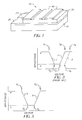
- FIG. 1 is an isometric partial view of a new structure for a display 10 made in accordance with the invention.
- Display 10 includes a flexible substrate 15, which is a thin transparent polymeric material, such as Kodak Estar film base formed of polyester plastic that has a thickness of between 20 and 200 microns.
- substrate 15 can be a 125 micron thick sheet of polyester film base.
- Other polymers, such as transparent polycarbonate, can also be used.
- Electrodes in the form of first patterned conductors 20 are formed over substrate 15.
- First patterned conductors 20 can be tin-oxide or indium-tin-oxide (ITO), with ITO being the preferred material.
- ITO indium-tin-oxide
- the material of first patterned conductors 20 is sputtered as a layer over substrate 15 having a resistance of less than 250 ohms per square.
- the layer is then patterned to form first patterned conductors 20 in any well known manner.
- first patterned conductors 20 can be an opaque electrical conductor material such as copper, aluminum or nickel. If first patterned conductors 20 are opaque metal, the metal can be a metal oxide to create light absorbing first patterned conductors 20.
- First patterned conductors 20 are formed in the conductive layer by conventional photolithographic or laser etching means.
- a polymer dispersed cholesteric layer 30 overlays first patterned conductors 20.
- Polymer dispersed cholesteric layer 30 includes a polymeric host material and dispersed cholesteric liquid crystal materials, such as those disclosed in US-A-5,695,682, the disclosure of which is incorporated by reference.
- Application of electrical fields of various amplitude and duration can drive a chiral nematic (cholesteric) material into a reflective state, a transmissive state, or an intermediate state.
- These cholesteric materials have the advantage of maintaining a given state indefinitely after the field is removed.
- Cholesteric liquid crystal materials can be Merck BL112, BL118 or BL126, available from EM Industries of Hawthorne, NY.
- the polymeric host material is provided by E.M. Industries cholesteric material BL-118 dispersed in deionized photographic gelatin.
- the liquid crystal material is dispersed at 8% concentration in a 5% deionized gelatin aqueous solution.
- the mixture is dispersed to create 10 micron diameter domains of the liquid crystal in aqueous suspension.
- the material is coated over a patterned ITO polyester sheet to provide a 7 micron thick polymer dispersed cholesteric coating.
- Other organic binders such as polyvinyl alcohol (PVA) or polyethylene oxide (PEO) can be used. Such compounds are machine coatable on equipment associated with photographic films.
- Second patterned conductors 40 should have sufficient conductivity to carry a field across polymer dispersed cholesteric layer 30.
- Second patterned conductors 40 can be formed in a vacuum environment using materials such as aluminum, silver, platinum, carbon, tungsten, molybdenum, tin or indium or combinations thereof.
- the second patterned conductors 40 are as shown in the form of a deposited layer. Oxides of said metals can be used to darken second patterned conductors 40.
- the metal material can be excited by energy from resistance heating, cathodic arc, electron beam, sputtering or magnetron excitation.
- Electrodes 20 and 40 disposed relative to polymer dispersed cholesteric layer 30 are in rows and columns so that the intersection of a row and column defines pixels for applying an electric field at each intersection to the polymer dispersed cholesteric layer 30 when a voltage is applied to the electrodes.
- second patterned conductors 40 are printed conductive ink such as Electrodag 423SS screen printable electrical conductive material from Acheson Corporation. Such printed materials are finely divided graphite particles in a thermoplastic resin.
- the second patterned conductors 40 are formed using the printed inks to reduce display cost.
- the use of a flexible support for substrate 15, laser etching to form first patterned conductors 20, machine coating polymer dispersed cholesteric layer 30, and printing second patterned conductors 40 permits the fabrication of very low cost memory displays. Small displays formed using these methods can be used as electronically rewritable tags for inexpensive, limited rewrite applications.
- FIG. 2A and FIG. 2B show two stable states of cholesteric liquid crystals.
- a high voltage field has been applied and quickly switched to zero potential, which converts cholesteric liquid crystal to a planar state 22.
- Incident light 26 striking cholesteric liquid crystal in planar state 22 is reflected as reflected light 28 to create a bright image.
- FIG. 2B application of a lower voltage field leaves cholesteric liquid crystal in a transparent focal conic state 24.
- Incident light 26 striking a cholesteric liquid crystal in focal conic state 24 is mainly forward scattered.
- Second patterned conductors 40 can be black which will absorb incident light 26 to create a dark image when the liquid crystal material is in focal conic state 24.
- cholesteric liquid crystal is in a homeotropic state 25 when a high voltage is applied.
- Incident light 26 illuminating a cholesteric liquid crystal in homeotropic state 25 is transmitted.
- FIG. 3 is a typical plot of reflectance response of a cholesteric material to the applied pulse voltage.
- Curve a is obtained when the cholesteric liquid crystal is initially in a planar state 22 and Curve b is obtained when the cholesteric liquid crystal is initially in a focal conic state 24. Both curves are measured at some time after the applied pulse is over. Such curves can be found in US-A-5,384,067, US-A-5,453,863, and US-A-5,695,682 and are also found in the above-cited Drzaic reference. For a given pulse time, typically between 5 and 200 milliseconds, a pulse at a given voltage can change the optical state of a cholesteric liquid crystal.
- bipolar voltage drive schemes are used for cholesteric displays to prevent ionic damage.
- the bipolar drives require at least two voltages and two separate semiconductor switching elements for each drive line.
- Curve a and Curve b lay on each other only when the pulse voltage is between V2 and V3, or greater than V4.
- V3 will hereinafter be referred to as the focal conic voltage or the off-voltage and V4 will be referred to as the planar voltage or the on-voltage.
- V4 will be referred to as the planar voltage or the on-voltage.
- the pulse voltage is between V2 and V3
- the cholesteric liquid crystal is driven into a focal conic state 24.
- the pulse voltage is above V4
- the cholesteric liquid crystal is first switched into a homeotropic state 25, and then relaxes into a planar state 22.
- there does not exist a common-voltage which can switch the cholesteric liquid crystal into the same gray scale image from either planar state 22 and focal conic state 24.
- Curve a and Curve b do not overlap between V3 and V4, an initial voltage pulse is required to drive all material into either planar state 22 or focal conic state 24 to form
- FIG. 4A schematically shows a method of prior art [Gandhi and others Asia Display 98, pp.127-130 (1998)] to achieve gray scale images.
- the cholesteric liquid crystal was first switched to a planar state 22 by a sufficiently high voltage above V4. Then the planar state 22 was selectively switched to different gray scale images based on Curve 1 by a pulsed voltage between V1 and V2 or Curve 2 by a pulsed voltage between V3 and V6 in FIG. 3.
- a second method to achieve gray scale images is shown in FIG. 4B.
- the cholesteric liquid crystal was first switch to a focal conic state 24 by a voltage between V2 and V3. Then the focal conic state 24 was selectively switched to different gray scale images by a pulsed voltage between V5 and V4 based on Curve 3 in FIG. 3.
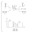
- FIG. 4C describes another third method of prior art (Huang and others SID Digest 98, pp.810-813 (1998)) to achieve a gray scale by a preparation phase 50 in which a sufficiently high voltage is applied, followed by a selection phase 51 and an evolution phase 52. An additional required pulse voltage phase such as 51 and 52 is not desirable.
- the current invention achieves gray scale images with a simple pulse voltage.
- FIG. 5 is a schematic plot of reflectance response of a display in accordance with the present invention to applied pulse voltage.
- Certain polymeric dispersed formulations have the unique property that both planar state 22 and focal conic state 24 share a common optical response (Curve 6) within the voltage between V3 and V4. In this range of voltage, the reflectance varies from the minimum to the maximum continuously independent of initial state.
- the cholesteric material changes to a state between the focal conic and planar states irrespective of the initial state of the material. Therefore, the cholesteric liquid crystals are effective in a number of different states of reflectivity and will remain in any given state until a field is applied.
- the initial state can be a planar state 22 (having a maximum reflectance), a focal conic state 24 (having a minimum reflectance), or any other intermediate state (having any gray level between the maximum reflectance and the minimum reflectance).
- FIG. 6A is experimental data of reflectance response of an experimental material to the applied pulse voltage.
- a set of curves was generated which correspond to different initial states, which were set by a 200 ms long DC pulse of 50% duty cycle and 1 kHz.
- Various pulse voltages were applied, including 45 V, 60 V, 70 V, 75 V, 80 V, 85 V, 90 V, and 95 V.
- the reflectance responses were substantially the same for all initial states.
- the cholesteric liquid crystals were converted to a particular state within a selected gray scale irrespective of the initial state of the cholesteric liquid crystals.
- the “substantially” means that the maximum difference in reflectance at peak wavelength from various initial states is within 1% of reflectance at any voltage between the focal conic voltage (60 V) and the planar voltage (90 V), and preferably the maximum difference is even smaller than 1% of reflectance. In this embodiment, the reflectance was 20% at 90 V, and 3% at 60 V. When the maximum difference in reflectance was within 1% of reflectance, more than 16 gray levels could be easily distinguished. This unique electro-optical property allowed the display to be converted to any gray scale state by amplitude modulation of a simple DC pulse.
- a gray scale state could also be achieved by pulse width modulation, namely, by adjusting the duration Toff of focal conic voltage V3 and the duration Ton of planar voltage V4 over the total pulse interval Ton+Toff.
- FIG. 6B shows that when focal conic voltage V3 and planar voltage V4 were chosen as 60 V and 90 V, respectively, the change in the ratio of Toff/(Ton+Toff) resulted in various gray scale states substantially regardless of its initial states.
- FIG. 6C shows that when focal conic voltage V3 and planar voltage V4 were chosen as 60 V and 95 V, the change in the ratio of Ton/(Ton+Toff) also led to various gray scale states, which were substantially independent of the initial state of the liquid crystal.
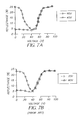
- planar state 22 and focal conic state 24 had different gray level responses to the voltage except for maximum and minimum reflectance as shown in FIG. 7A and FIG. 7B.
- the pulse was DC
- FIG. 7B the pulse was AC.
- the electric field pulse is preferably a DC pulse.
- the DC pulse can be a continuous pulse (single pulse), which is fully characterized by pulse width t0 and amplitude, as shown in FIG. 8A.
- a DC voltage pulse can consist of a series of sub continuous DC voltage pulses, which is characterized by pulse width t0, duty cycle t2/t1, frequency 1/t1, as well as amplitude.
- the duty cycle is the ratio of the effective time duration over the total pulse width.
- FIG. 8B discloses a series of DC voltage pulses that can be used in accordance with the present invention.
- FIG. 8D shows an AC pulse consisting of a series of sub voltage pulses characterized by pulse width t0, fraction of positive polarity t2/t1, frequency 1/t1, as well as amplitude.
- FIG.8C shows that each sub DC pulse can have its own sub DC pulses, with each characterized by pulse width t2, duty cycle t4/t3, frequency 1/t3, as well as amplitude.
- the ratios t1/t2 and t3/t4 are preferred to be integral numbers.
- the DC pulse used is described by FIG. 8B, a few of rows up to t1/t2 can be grouped together to be selected. During the voltage pulse goes to zero for one row, the voltage pulse can be applied to the next few rows up to t1/2-1. Therefore, the effective driving time for each line is actually the total pulse time t0 multiplied by duty cycle t2/t1.
- FIG. 9A shows the waveforms for amplitude modulation.
- the gray scale images of the display is created by varying voltage amplitude between focal conic voltage and planar voltage.
- FIG. 9B shows the voltage pulse first consists of focal conic voltage V3 and then followed by planar voltage V4.
- FIG. 9C shows the voltage pulse first consists of focal conic voltage V3 followed by planar voltage V4, and then followed by focal conic voltage V3.
- FIG. 9D shows the voltage pulse first consists of planar voltage V4 and then followed by focal conic voltage V3.
- gelatin dispersed cholesteric liquid crystal material was coated over ITO coated flexible substrate 15 to form polymer dispersed cholesteric layer 30.
- a small amount of surfactant was added in the dispersion to make the coating uniform.
- a one-inch square conductive patch was printed over the gelatin dispersed cholesteric material to provide a field across the coating.
- the cholesteric liquid crystal was BL118 from Merck, which reflected green light.
- the weight ratio of the cholesteric liquid crystal, the gelatin, and the surfactant was 8:5:1. The mixture was homogenized to create about 10 micron domains of the liquid crystal in aqueous suspension.
- a substantially common gray scale response of this display was achieved by a 70 millisecond DC pulse of duty cycle 50% and frequency 20 Hz. The same response was found using 140 millisecond DC pulse of duty cycle 20% and frequency 50 Hz. Furthermore a common response was found using 140 millisecond DC pulse of duty cycle 25% and frequency 100 Hz, or 500 millisecond DC pulse of duty cycle 100%. Other driving parameters could be found by those skilled in the art.
- a display patch was prepared as in Example 1, except that the ratio of the cholesteric liquid crystal, the gelatin, and the surfactant varied. The ratios were 1:1:0.06, 1.6:1:0.06, 2.4:1:0.6, and 4:1:0.6, respectively.
- the dry coating thickness varied from 2.6 microns to 13.3 microns. A substantially same gray scale response of this display from different initial states made as above described was obtained driven using proper DC driving parameters. A larger dry thickness enhances reflectance, but also increases driving voltage.
- the layer including a polymeric host material and cholesteric liquid crystals prefers to have a dry thickness less than 15 microns.
- a display patch was prepared as in Example 1, except that the size of liquid crystal domains in aqueous suspension varied from 4.8 to 16.1 microns. This size was measured before the dispersion was coated over ITO coated PET film. A substantially same gray scale response of this display from different initial states made as above described was obtained driven using proper DC driving parameters.
- there is an optimized domain size for the liquid crystal for a given ratio of gelatin and cholesteric liquid crystal.
- the liquid crystal domain size is preferably selected to be in a range of 4 to 20 microns.
- Displays according to the invention were tested using a 20 millisecond unipolar field switched across display 10 every 5 seconds to switch the state of the material between the planar and focal conic states.
- the gelatin dispersed cholesteric material was driven through a limited life test of 10,000 rewrites. The life testing was equivalent to 200 seconds of continuous applied unipolar voltage to display 10. The test patch operated with no apparent visible degradation throughout the life test. The life test was then extended to 100,000 cycles. The test display 10 continued to perform with little degradation. From this experiment, it was concluded that polymeric dispersed cholesteric materials on flexible substrates 15 with printed conductors can be driven by unipolar (DC) fields for at least the limited number of life cycles needed for limited-life display applications. Such displays benefit from a drive scheme that uses inexpensive, simple switching chips operating on a single voltage.
- a color display can be made in accordance with the invention, which is comprised of a plurality of displays, which are discussed above.
- the cholesteric liquid crystals in the different displays will produce a different color so that a multicolored image can be produced.
Landscapes
- Physics & Mathematics (AREA)
- Chemical & Material Sciences (AREA)
- Crystallography & Structural Chemistry (AREA)
- Nonlinear Science (AREA)
- General Physics & Mathematics (AREA)
- Engineering & Computer Science (AREA)
- Optics & Photonics (AREA)
- Computer Hardware Design (AREA)
- Theoretical Computer Science (AREA)
- Liquid Crystal (AREA)
- Devices For Indicating Variable Information By Combining Individual Elements (AREA)
Applications Claiming Priority (2)
| Application Number | Priority Date | Filing Date | Title |
|---|---|---|---|
| US923659 | 2001-08-07 | ||
| US09/923,659 US6816227B2 (en) | 2001-08-07 | 2001-08-07 | Gray scale and color cholesteric liquid crystal displays |
Publications (2)
| Publication Number | Publication Date |
|---|---|
| EP1283435A2 true EP1283435A2 (fr) | 2003-02-12 |
| EP1283435A3 EP1283435A3 (fr) | 2003-05-21 |
Family
ID=25449046
Family Applications (1)
| Application Number | Title | Priority Date | Filing Date |
|---|---|---|---|
| EP02078067A Withdrawn EP1283435A3 (fr) | 2001-08-07 | 2002-07-26 | Dispositif d'affichage en niveaux de gris et en couleurs à cristaux liquides cholestériques |
Country Status (3)
| Country | Link |
|---|---|
| US (1) | US6816227B2 (fr) |
| EP (1) | EP1283435A3 (fr) |
| JP (1) | JP4316202B2 (fr) |
Cited By (4)
| Publication number | Priority date | Publication date | Assignee | Title |
|---|---|---|---|---|
| US20050253875A1 (en) * | 2004-05-14 | 2005-11-17 | Eastman Kodak Company | Driving scheme for cholesteric liquid crystal display |
| WO2006051273A1 (fr) * | 2004-11-10 | 2006-05-18 | Magink Display Tecnologies Ltd. | Schema d'excitation pour un ecran a cristaux liquides cholesteriques |
| WO2007110582A3 (fr) * | 2006-03-29 | 2007-11-29 | Isis Innovation | Dispositif à cristaux liquides et procédé de commande d'un tel dispositif |
| EP2538403A3 (fr) * | 2008-09-24 | 2013-01-09 | 3M Innovative Properties Company | Schéma de commande d'échelle de gris unipolaire pour affichages à cristaux liquides cholestériques |
Families Citing this family (23)
| Publication number | Priority date | Publication date | Assignee | Title |
|---|---|---|---|---|
| US20030085863A1 (en) * | 2001-11-03 | 2003-05-08 | Yao-Dong Ma | Dynamic -relaxation driving means for cholesteric liquid crystal displays |
| IL152029A0 (en) * | 2002-09-30 | 2003-04-10 | Magink Display Technologies | Distinct color lcd apparatus |
| US6950157B2 (en) * | 2003-06-05 | 2005-09-27 | Eastman Kodak Company | Reflective cholesteric liquid crystal display with complementary light-absorbing layer |
| US7737928B2 (en) * | 2003-07-02 | 2010-06-15 | Kent Displays Incorporated | Stacked display with shared electrode addressing |
| US7236151B2 (en) * | 2004-01-28 | 2007-06-26 | Kent Displays Incorporated | Liquid crystal display |
| US7432895B2 (en) * | 2003-10-02 | 2008-10-07 | Industrial Technology Research Institute | Drive for active matrix cholesteric liquid crystal display |
| US20050076889A1 (en) * | 2003-10-14 | 2005-04-14 | Melendrez Julian B. | Fuel conditioning device |
| CN1914031B (zh) * | 2004-01-28 | 2011-11-16 | 肯特显示器公司 | 可悬垂液晶转移显示膜 |
| GB2427302B (en) * | 2004-01-28 | 2008-10-15 | Incorporated Kent Displays | Liquid crystal display films |
| US8199086B2 (en) * | 2004-01-28 | 2012-06-12 | Kent Displays Incorporated | Stacked color photodisplay |
| US20050237473A1 (en) * | 2004-04-27 | 2005-10-27 | Stephenson Stanley W | Coatable conductive layer |
| IL165150A0 (en) * | 2004-11-10 | 2005-12-18 | Magink Display Technologies | A cholesteric liquid crystal display device |
| US20060202925A1 (en) * | 2004-12-07 | 2006-09-14 | William Manning | Remote cholesteric display |
| FR2885425B1 (fr) * | 2005-05-09 | 2008-07-04 | Eastman Kodak Co | Dispositif d'ecriture et d'affichage electronique reutilisable |
| US7791700B2 (en) * | 2005-09-16 | 2010-09-07 | Kent Displays Incorporated | Liquid crystal display on a printed circuit board |
| WO2008023415A1 (fr) * | 2006-08-23 | 2008-02-28 | Fujitsu Limited | Élément d'affichage à cristaux liquides, son procédé de commande et papier électronique associé |
| GB0702977D0 (en) * | 2007-02-15 | 2007-03-28 | Magink Display Technologies In | Driving of a cholesteric liquid display apparatus |
| US20100156878A1 (en) * | 2008-12-18 | 2010-06-24 | Industrial Technology Research Institute | Systems for driving displays |
| US20130016131A1 (en) * | 2011-07-15 | 2013-01-17 | Industrial Technology Research Institute | Driving method of multi-stable display |
| US10871694B2 (en) * | 2016-09-09 | 2020-12-22 | Kent State University | Bistable cholesteric liquid crystal switchable window |
| WO2023129370A1 (fr) | 2021-12-30 | 2023-07-06 | Corning Incorporated | Fenêtre à cristaux liquides cholestériques ayant de multiples états stables et procédés d'utilisation |
| TWI876826B (zh) * | 2024-01-08 | 2025-03-11 | 友達光電股份有限公司 | 膽固醇液晶顯示器及其驅動方法 |
| CN121306062A (zh) * | 2025-12-15 | 2026-01-09 | 安徽煜图科技有限公司 | 一种多灰阶胆甾相液晶显示装置及其驱动方法 |
Family Cites Families (14)
| Publication number | Priority date | Publication date | Assignee | Title |
|---|---|---|---|---|
| US4435047A (en) | 1981-09-16 | 1984-03-06 | Manchester R & D Partnership | Encapsulated liquid crystal and method |
| US5695682A (en) | 1991-05-02 | 1997-12-09 | Kent State University | Liquid crystalline light modulating device and material |
| EP0582656B1 (fr) | 1991-05-02 | 1999-04-07 | Kent State University | Dispositif et materiau modulateurs de lumiere a cristaux liquides |
| US5453863A (en) | 1991-05-02 | 1995-09-26 | Kent State University | Multistable chiral nematic displays |
| US5251048A (en) | 1992-05-18 | 1993-10-05 | Kent State University | Method and apparatus for electronic switching of a reflective color display |
| DE69229003T2 (de) | 1992-05-18 | 1999-10-21 | Kent State University, Kent | Flüssigkristalline, lichtmodulierende vorrichtung und material |
| EP0674208A1 (fr) | 1994-03-22 | 1995-09-27 | Shinto Paint Co., Ltd. | Méthode pour la fabrication d'un filtre coloré et d'un dispositif d'affichage à cristal liquide |
| US5644330A (en) | 1994-08-11 | 1997-07-01 | Kent Displays, Inc. | Driving method for polymer stabilized and polymer free liquid crystal displays |
| US5748277A (en) | 1995-02-17 | 1998-05-05 | Kent State University | Dynamic drive method and apparatus for a bistable liquid crystal display |
| US6061107A (en) | 1996-05-10 | 2000-05-09 | Kent State University | Bistable polymer dispersed cholesteric liquid crystal displays |
| AU7703900A (en) * | 1999-09-17 | 2001-04-17 | Three-Five Systems, Inc. | Drive system for cholesteric display |
| US6556262B1 (en) * | 2000-01-06 | 2003-04-29 | Eastman Kodak Company | Display sheet having memory using limited coalescence domains |
| US6423368B1 (en) * | 2000-01-06 | 2002-07-23 | Eastman Kodak Company | Method for making materials having uniform limited coalescence domains |
| US6667785B2 (en) * | 2001-01-17 | 2003-12-23 | Eastman Kodak Company | Providing a color image in a light modulating layer having liquid crystal domains |
-
2001
- 2001-08-07 US US09/923,659 patent/US6816227B2/en not_active Expired - Lifetime
-
2002
- 2002-07-26 EP EP02078067A patent/EP1283435A3/fr not_active Withdrawn
- 2002-08-06 JP JP2002229015A patent/JP4316202B2/ja not_active Expired - Fee Related
Cited By (7)
| Publication number | Priority date | Publication date | Assignee | Title |
|---|---|---|---|---|
| US20050253875A1 (en) * | 2004-05-14 | 2005-11-17 | Eastman Kodak Company | Driving scheme for cholesteric liquid crystal display |
| WO2005114633A1 (fr) * | 2004-05-14 | 2005-12-01 | Eastman Kodak Company | Mecanisme d'entrainement pour affichage a cristaux liquides cholesteriques |
| US7432899B2 (en) | 2004-05-14 | 2008-10-07 | Industrial Technology Research Institute | Driving scheme for cholesteric liquid crystal display |
| WO2006051273A1 (fr) * | 2004-11-10 | 2006-05-18 | Magink Display Tecnologies Ltd. | Schema d'excitation pour un ecran a cristaux liquides cholesteriques |
| US8013819B2 (en) | 2004-11-10 | 2011-09-06 | Magink Display Technologies Ltd | Drive scheme for a cholesteric liquid crystal display device |
| WO2007110582A3 (fr) * | 2006-03-29 | 2007-11-29 | Isis Innovation | Dispositif à cristaux liquides et procédé de commande d'un tel dispositif |
| EP2538403A3 (fr) * | 2008-09-24 | 2013-01-09 | 3M Innovative Properties Company | Schéma de commande d'échelle de gris unipolaire pour affichages à cristaux liquides cholestériques |
Also Published As
| Publication number | Publication date |
|---|---|
| US6816227B2 (en) | 2004-11-09 |
| US20030034945A1 (en) | 2003-02-20 |
| JP4316202B2 (ja) | 2009-08-19 |
| JP2003131196A (ja) | 2003-05-08 |
| EP1283435A3 (fr) | 2003-05-21 |
Similar Documents
| Publication | Publication Date | Title |
|---|---|---|
| US6816227B2 (en) | Gray scale and color cholesteric liquid crystal displays | |
| EP1258860B1 (fr) | Circuit de commande pour un dispositif d'affichage à cristaux liquides cholestériques | |
| EP1324106B1 (fr) | Couche adaptée pour distribuer le champ électrique de revêtements à cristaux liquides dispersés | |
| US6894668B2 (en) | General 2 voltage levels driving scheme for cholesterical liquid crystal displays | |
| US20130141655A1 (en) | Common Transparent Electrode for Reduced Voltage Displays | |
| US7307608B2 (en) | Unipolar drive chip for cholesteric liquid crystal displays | |
| EP1058147A2 (fr) | Feuille multicouche à double polarité pour la modulation de la lumière | |
| EP1324107B1 (fr) | Couche transparente adaptée pour disperser le champ électrique de revêtements à cristaux liquides dispersés | |
| US6710760B1 (en) | Unipolar drive for cholesteric liquid crystal displays | |
| US6690447B1 (en) | Liquid-crystal display comprising a dielectric layer between electrodes and methods for making the same | |
| US6885357B2 (en) | Method for writing pixels in a cholesteric liquid crystal display | |
| US7432899B2 (en) | Driving scheme for cholesteric liquid crystal display | |
| US7522141B2 (en) | Cholesteric liquid crystal display system | |
| US6924783B2 (en) | Drive scheme for cholesteric liquid crystal displays |
Legal Events
| Date | Code | Title | Description |
|---|---|---|---|
| PUAI | Public reference made under article 153(3) epc to a published international application that has entered the european phase |
Free format text: ORIGINAL CODE: 0009012 |
|
| AK | Designated contracting states |
Designated state(s): AT BE BG CH CY CZ DE DK EE ES FI FR GB GR IE IT LI LU MC NL PT SE SK TR |
|
| AX | Request for extension of the european patent |
Extension state: AL LT LV MK RO SI |
|
| PUAL | Search report despatched |
Free format text: ORIGINAL CODE: 0009013 |
|
| AK | Designated contracting states |
Designated state(s): AT BE BG CH CY CZ DE DK EE ES FI FR GB GR IE IT LI LU MC NL PT SE SK TR |
|
| AX | Request for extension of the european patent |
Extension state: AL LT LV MK RO SI |
|
| 17P | Request for examination filed |
Effective date: 20031024 |
|
| 17Q | First examination report despatched |
Effective date: 20031127 |
|
| AKX | Designation fees paid |
Designated state(s): DE FR GB |
|
| RAP1 | Party data changed (applicant data changed or rights of an application transferred) |
Owner name: INDUSTRIAL TECHNOLOGY RESEARCH INSTITUTE |
|
| APBK | Appeal reference recorded |
Free format text: ORIGINAL CODE: EPIDOSNREFNE |
|
| APBN | Date of receipt of notice of appeal recorded |
Free format text: ORIGINAL CODE: EPIDOSNNOA2E |
|
| APBR | Date of receipt of statement of grounds of appeal recorded |
Free format text: ORIGINAL CODE: EPIDOSNNOA3E |
|
| APAF | Appeal reference modified |
Free format text: ORIGINAL CODE: EPIDOSCREFNE |
|
| APBT | Appeal procedure closed |
Free format text: ORIGINAL CODE: EPIDOSNNOA9E |
|
| STAA | Information on the status of an ep patent application or granted ep patent |
Free format text: STATUS: THE APPLICATION IS DEEMED TO BE WITHDRAWN |
|
| 18D | Application deemed to be withdrawn |
Effective date: 20140201 |