EP1283543A1 - Dispositif d'affichage a decharge plat - Google Patents
Dispositif d'affichage a decharge plat Download PDFInfo
- Publication number
- EP1283543A1 EP1283543A1 EP02711229A EP02711229A EP1283543A1 EP 1283543 A1 EP1283543 A1 EP 1283543A1 EP 02711229 A EP02711229 A EP 02711229A EP 02711229 A EP02711229 A EP 02711229A EP 1283543 A1 EP1283543 A1 EP 1283543A1
- Authority
- EP
- European Patent Office
- Prior art keywords
- glass substrate
- discharge display
- projection
- display portions
- front glass
- Prior art date
- Legal status (The legal status is an assumption and is not a legal conclusion. Google has not performed a legal analysis and makes no representation as to the accuracy of the status listed.)
- Withdrawn
Links
- 239000011521 glass Substances 0.000 claims abstract description 170
- 239000000758 substrate Substances 0.000 claims abstract description 127
- 239000000126 substance Substances 0.000 claims description 15
- 238000003486 chemical etching Methods 0.000 claims description 5
- 230000003247 decreasing effect Effects 0.000 abstract description 3
- 125000006850 spacer group Chemical group 0.000 abstract description 3
- 239000007789 gas Substances 0.000 description 10
- 239000010410 layer Substances 0.000 description 10
- 238000000034 method Methods 0.000 description 9
- 239000000463 material Substances 0.000 description 4
- 238000007650 screen-printing Methods 0.000 description 4
- 108010043121 Green Fluorescent Proteins Proteins 0.000 description 3
- 239000005394 sealing glass Substances 0.000 description 3
- XKRFYHLGVUSROY-UHFFFAOYSA-N Argon Chemical compound [Ar] XKRFYHLGVUSROY-UHFFFAOYSA-N 0.000 description 2
- 239000003086 colorant Substances 0.000 description 2
- 239000005357 flat glass Substances 0.000 description 2
- 239000011159 matrix material Substances 0.000 description 2
- 238000002844 melting Methods 0.000 description 2
- 230000002093 peripheral effect Effects 0.000 description 2
- FYYHWMGAXLPEAU-UHFFFAOYSA-N Magnesium Chemical compound [Mg] FYYHWMGAXLPEAU-UHFFFAOYSA-N 0.000 description 1
- 239000000853 adhesive Substances 0.000 description 1
- 230000001070 adhesive effect Effects 0.000 description 1
- 229910052786 argon Inorganic materials 0.000 description 1
- 239000011248 coating agent Substances 0.000 description 1
- 238000000576 coating method Methods 0.000 description 1
- 238000007599 discharging Methods 0.000 description 1
- 238000010030 laminating Methods 0.000 description 1
- 238000003475 lamination Methods 0.000 description 1
- 229910052749 magnesium Inorganic materials 0.000 description 1
- 239000011777 magnesium Substances 0.000 description 1
- 238000004519 manufacturing process Methods 0.000 description 1
- 229910052754 neon Inorganic materials 0.000 description 1
- GKAOGPIIYCISHV-UHFFFAOYSA-N neon atom Chemical compound [Ne] GKAOGPIIYCISHV-UHFFFAOYSA-N 0.000 description 1
- 238000007639 printing Methods 0.000 description 1
- 239000011241 protective layer Substances 0.000 description 1
- 229910052724 xenon Inorganic materials 0.000 description 1
- FHNFHKCVQCLJFQ-UHFFFAOYSA-N xenon atom Chemical compound [Xe] FHNFHKCVQCLJFQ-UHFFFAOYSA-N 0.000 description 1
Images


Classifications
-
- H—ELECTRICITY
- H01—ELECTRIC ELEMENTS
- H01J—ELECTRIC DISCHARGE TUBES OR DISCHARGE LAMPS
- H01J11/00—Gas-filled discharge tubes with alternating current induction of the discharge, e.g. alternating current plasma display panels [AC-PDP]; Gas-filled discharge tubes without any main electrode inside the vessel; Gas-filled discharge tubes with at least one main electrode outside the vessel
- H01J11/20—Constructional details
- H01J11/48—Sealing, e.g. seals specially adapted for leading-in conductors
-
- H—ELECTRICITY
- H01—ELECTRIC ELEMENTS
- H01J—ELECTRIC DISCHARGE TUBES OR DISCHARGE LAMPS
- H01J11/00—Gas-filled discharge tubes with alternating current induction of the discharge, e.g. alternating current plasma display panels [AC-PDP]; Gas-filled discharge tubes without any main electrode inside the vessel; Gas-filled discharge tubes with at least one main electrode outside the vessel
- H01J11/10—AC-PDPs with at least one main electrode being out of contact with the plasma
- H01J11/14—AC-PDPs with at least one main electrode being out of contact with the plasma with main electrodes provided only on one side of the discharge space
-
- H—ELECTRICITY
- H01—ELECTRIC ELEMENTS
- H01J—ELECTRIC DISCHARGE TUBES OR DISCHARGE LAMPS
- H01J11/00—Gas-filled discharge tubes with alternating current induction of the discharge, e.g. alternating current plasma display panels [AC-PDP]; Gas-filled discharge tubes without any main electrode inside the vessel; Gas-filled discharge tubes with at least one main electrode outside the vessel
- H01J11/20—Constructional details
- H01J11/22—Electrodes, e.g. special shape, material or configuration
-
- H—ELECTRICITY
- H01—ELECTRIC ELEMENTS
- H01J—ELECTRIC DISCHARGE TUBES OR DISCHARGE LAMPS
- H01J11/00—Gas-filled discharge tubes with alternating current induction of the discharge, e.g. alternating current plasma display panels [AC-PDP]; Gas-filled discharge tubes without any main electrode inside the vessel; Gas-filled discharge tubes with at least one main electrode outside the vessel
- H01J11/20—Constructional details
- H01J11/34—Vessels, containers or parts thereof, e.g. substrates
- H01J11/36—Spacers, barriers, ribs, partitions or the like
-
- H—ELECTRICITY
- H01—ELECTRIC ELEMENTS
- H01J—ELECTRIC DISCHARGE TUBES OR DISCHARGE LAMPS
- H01J11/00—Gas-filled discharge tubes with alternating current induction of the discharge, e.g. alternating current plasma display panels [AC-PDP]; Gas-filled discharge tubes without any main electrode inside the vessel; Gas-filled discharge tubes with at least one main electrode outside the vessel
- H01J11/20—Constructional details
- H01J11/34—Vessels, containers or parts thereof, e.g. substrates
- H01J11/42—Fluorescent layers
Definitions
- the present invention relates to a planar discharge display device in which glass frits are coated not only around a front glass substrate and a rear glass substrate but also on the spaces between a plurality of unit discharge display portions and the adjacent unit discharge display portions of a front glass substrate and then the front glass substrate and a rear glass substrate are joined by the glass frits to thereby form a flat tube-assembly.
- a front glass substrate and a rear glass substrate in which respective members such as electrodes, ribs and fluorescent substances are provided are opposed to each other and are brought in contact with each other such that respective members are assembled together in a predetermined relationship and the surrounding portions of the two glass substrates are joined by glass frits and sealed in vacuum, thereby forming a planar discharge display device having a flat tube-assembly.
- a frit coating width of a certain width i.e., so-called margin is required in order to maintain adhesive strength.
- a width of this margin generally ranges approximately several millimeters to 10 millimeters.
- the assignee of the present application has previously proposed a planar discharge display device in which glass frits are coated not only on the surrounding portions of the front glass substrates and the rear glass substrates but also on spaces between unit discharge display portions of a plurality of unit discharge display portions [one cell or a plurality of discharge cells (pixel of single color or pixel comprising a set of three primary colors)] of a front glass substrate and a rear glass substrate and adjacent discharge display portions and the front glass substrate and the rear glass substrate are joined by such glass frits to thereby form a flat tube-assembly [see (Japanese patent application No. 7-317626) and (Japanese laid-open patent application No. 9-129143)].
- a plurality of unit discharge display portions are provided in an XY matrix fashion.
- the glass frits are coated on not only the surrounding portions of the front glass substrate and the rear glass substrate but also on the spaces between a plurality of unit discharge display portions and the adjacent to join the front glass substrate and the rear glass substrate, distortions and stress of the front glass substrate and the rear glass substrate are dispersed and burden imposed upon the frits coated on the surrounding portions of the front glass substrate and the rear glass substrate can be reduced considerably. Therefore, the widths of the glass frits coated on the surrounding portions of the front glass substrate and the rear glass substrate can be minimized.
- a planar discharge display device in which glass frit is coated on the surrounding portions of the rear glass substrate and the front glass substrate, glass frit is also coated on the spaces between a plurality of unit discharge display portions and the adjacent unit discharge display portions of the rear glass substrate and the front glass substrate and then the rear glass substrate and the front glass substrate are joined with pressure under the condition in which glass frit is being heated to thereby form a vacuum flat tube-assembly into which discharge gas is filled.
- this planar discharge display device there can be removed risks in which crosstalk is caused by erroneous discharge and in which bonding failure is caused due to uneven thickness of glass frits.
- a planar discharge display device including projection-like structure members provided in spaces between a plurality of unit discharge display portions and the adjacent unit discharge display portions of one and the other of a rear glass substrate and a front glass substrate, recesses engaged with the projection-like structure members and glass frits coated on the surrounding portions of the rear glass substrate and the front glass substrate and coated between the proj ection-like structure members and the recesses which are respectively engaged with the projection-like structure members, in which the rear glass substrate and the front glass substrates are joined with pressure under the condition in which glass frit is being heated to thereby form a vacuum flat tube-assembly into which discharge gas is filled.
- a planar discharge display device including recesses formed on spaces between a plurality of unit discharge display portions and unit discharge display portions adjoining to the respective unit discharge display portions of a front glass substrate and portions coated with fluorescent substances by sandblast or chemical etching, projection-like structure members respectively engaged with the recesses formed on the spaces between a plurality of unit discharge display portions and the unit discharge display portions adjoining to the respective unit discharge display portions and which are also engaged with the recesses formed on the spaces between a plurality of unit discharge display portions and the unit discharge display portions adjoining to the respective unit discharge display portions, fluorescent substances coated on the front glass substrate at its recesses coated with fluorescent substances and glass frits provided on the surrounding portions of the rear glass substrate and the front glass substrate and between the recesses and the respective projection-like structure members engaged with the respective recesses, in which the rear glass substrate and the front glass substrate are joined with pressure under the condition in which glass frit is being heated to thereby form a vacuum flat tube-assembly into which discharge gas
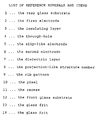
- FIG. 1 is a perspective view showing a planar display device according to an embodiment of the present invention in an exploded fashion.
- FIG. 2 is a fragmentary cross-sectional view showing a planar display device according to an embodiment of the present invention.
- FIG. 3 is a fragmentary cross-sectional view showing a planar display device according to another embodiment of the present invention.
- FIG. 1 is an exploded perspective view of a planar discharge display device
- FIG. 2 is a fragmentary cross-sectional view thereof.
- Projection-like structure members 8 formed on a rear glass substrate 1 and recesses 11 formed on a front glass substrate 12 characterize a planar discharge display device according to this embodiment.
- the projection-like structure members 8 may be formed on the front glass substrate 12 and the recesses 11 may be formed on the front glass substrate 1.
- the projection-like structure member 8 and the recess 11 are opposed to each other. As shown in FIG. 2, the projection-like structure member 8 and the recess 11 are shaped so as to be engaged with each other and joined by glass frit 13 interposed between the projection-like structure member 8 and the recess 11.
- peripheral portions of the rear glass substrate 1 and the front glass substrate 12 are coated with another end-sealing glass frit 14.
- discharge electrodes 2, 5 and 6 which are formed on the rear glass substrate 1 as shown in FIG. 1 are not directly related to the glass joint structure which is one of the characteristics of the present invention and are only examples for use in explaining the present invention, these discharge electrodes will be described below.
- a plurality of first electrodes 2 is formed on the rear glass substrate 1 in parallel to each other by a suitable method such as screen-printing.
- an insulating layer 3 is formed so as to cover a plurality of first electrodes 2.
- the insulating layer 3 has through-holes 4 defined thereon.
- the through-holes 4 can be easily formed by a screen mask with a through-hole pattern at the same time the insulating layer 3 is formed with the screen mask by screen printing or the like.
- a plurality of second electrodes 6 are formed on the insulating layer 3 in parallel to each other in such that they may cross a plurality of first electrodes 2, and a plurality of slit-like electrodes 5 are formed on the insulating layer through the through-holes 4 in such a manner that they may be connected to a plurality of electrodes 2, respectively.
- the first and second electrodes 2 and 6 form an XY matrix, which may cross each other through the insulating layer 3.
- discharge is generated between a selected electrode of a plurality of second electrodes 6 and a selected electrode of a plurality of slit-like electrodes 5.
- a plurality of second electrodes 6 are covered with a dielectric layer 7 and the dielectric layer 7 is covered with a protective layer (not shown) such as oxide magnesium and thereby an AC discharge electrodes are formed.
- a plurality of second electrodes may form DC electrodes without the dielectric layer 7.
- a plurality of projection-like structure members 8 are formed on the dielectric layer 7.
- the projection-like structure members 8 can be easily formed at high accuracy by effecting lamination screen-printing on a suitable material such as low-melting glass.
- the projection-like structure members 8 may be shaped freely so long as they can be fitted into the recesses 11 formed on the front glass substrate 12, which will be described later on, e.g., they may be shaped like plates, hemispheres and so on. Stated otherwise, the recesses 11 may be shaped in such a manner that they can be fitted into the projection-like structure members 8.
- the joint frit 13 is coated on the upper surface of the projection-like structure members or the body of the projection-like structure members 8 and temporarily dried.
- the joint glass frit may be the same material as that of end-sealing glass frit 14 which is used to end-seal the peripheral portions of the rear glass substrate and the front glass substrate in the vacuum state or may be a different material depending upon the manufacturing process.
- a proper height of the projection-like structure member 8 may fall within a range of from approximately 0.1 mm to approximately 0.2 mm when a thickness of rib patterns 9 on the front glass substrate 12 and a thickness of the joint glass frit 14 are considered as shown in FIG. 3.
- the front glass substrate 12 has formed thereon a set of three recesses for use as a set of three pixels 10 which are respectively coated with red, blue and green fluorescent substances, and red, blue and green fluorescent substances may be coated on the recesses for use as a set of three pixels 10 and thereby a set of pixels 10 comprising the red, blue and green fluorescent substances are formed.
- the unit discharge display portion is composed of one or a plurality of discharge cells (pixel of single color or pixel formed of a set of three primary colors).
- the recess 11 engaged with the projection-like structure member 8 of the rear glass substrate 1 side is formed on the portion between the pixel 10 and the adjacent pixel.
- These pixel 10 and recess 11 are formed by a method similar to that, which is used to form a rib (rib) in an ordinary PDP.
- a rib rib
- low-melting glass may be laminated with patterns by printing or rib members having a proper thickness, e.g., approximately ranging from 0.1 mm to 0.2 mm may be laminated on the whole and the laminated rib members maybe treated with patterns by a suitable method such as sandblast.
- the ordinary rib pattern 9 is made of a black material in order to improve contrast. Fluorescent substances are coated on the recess of the pixel 10 thus formed by a suitable method such as screen-printing and bonding glass frit 13 is coated on the recess 11.
- a plurality of projection-like structure members 8 and a plurality of recesses 11 which had been formed on the rear glass substrate 1 and the front glass substrate 12 in which respective members are formed are respectively engaged with each other through the glass frits 13. Further, the end-sealing glass frits 14 are coated on the surrounding portions of the rear glass substrate 1 and the front glass substrate 12. Thereafter, when the whole of the resultant product is heated at about 450°C, the glass frits 13 and 14 are melted to bond the two glass substrates 1, 12 and an air-tight flat tube-assembly which is vacuum tolerable in the inside can be constructed of the rear glass substrate 1 and the front glass substrate 12.
- gas necessary for discharging e.g., a mixed gas such as neon gas, argon gas or xenon gas is filled into the flat tube-assembly and thereby the planar discharge display device is formed.
- a mixed gas such as neon gas, argon gas or xenon gas
- planar discharge display device is different from the planar discharge display device, which has been described so far with reference to FIGS. 1 and 2 in a method of forming the recess 11 and the pixel 10 on the front glass substrate 12 side.
- the recess 11 of the planar discharge display device and the recess of the pixel 10 shown in FIGS. 1 and 2 are formed by laminating the rib members on the flat plate glass
- the recess 11 and the recess of the pixel 10 are formed by directly engraving the front glass substrate 12 in accordance with a proper method such as sandblast or chemical etching.
- this recess 11 and the recess of the pixel 10 may be formed in such a manner that a photosensitive resist film is deposited on a plate glass and a pattern to be formed is exposed and developed, whereafter they are formed by sandblast or chemical etching.
- Processes following the processes in which respective recesses had been formed are similar to those of the planar discharge display device, which has been described so far with reference to FIGS. 1 and 2.
- a planar discharge display device includes projection-like structure members provided in spaces between a plurality of unit discharge display portions and the adjacent unit discharge display portions of one and the other of a rear glass substrate and a front glass substrate, recesses engaged with the projection-like structure members and glass frits coated on the surrounding portions of the rear glass substrate and the front glass substrate, the respective projection-like structure members and the recesses in which the rear glass substrate and the front glass substrates are joined with pressure under the condition in which glass frit is being heated to thereby form a vacuum flat tube-assembly into which discharge gas is filled, there can be removed a risk in which the space between the rear glass substrate and the front glass substrate will cause erroneous discharge to occur to generate crosstalk or a risk in which bonding failure will be caused by uneven thickness of the glass frit.
- a planar discharge display device includes recesses formed on spaces between a plurality of unit discharge display portions and unit discharge display portions adjoining to the respective unit discharge display portions of a front glass substrate and portions coated with fluorescent substances by sandblast or chemical etching, projection-like structure members respectively engaged with the recesses formed on the spaces among a plurality of unit discharge display portions and the unit discharge display portions adjoining to the respective unit discharge display portions and which are also engaged with the recesses formed on the spaces between a plurality of unit discharge display portions and the unit discharge display portions adjoining to the respective unit discharge display portions, fluorescent substances coated on the front glass substrate at its recesses coated with fluorescent substances and glass frits provided on the surrounding portions of the rear glass substrate and the front glass substrate, the respective recesses and between the respective projection-like structure members engaged with the respective recesses in which the rear glass substrate and the front glass substrate are joined with pressure under the condition in which glass frit is being heated to thereby form a vacuum flat tube-assembly into which discharge gas is filled
Landscapes
- Engineering & Computer Science (AREA)
- Physics & Mathematics (AREA)
- Plasma & Fusion (AREA)
- Chemical & Material Sciences (AREA)
- Materials Engineering (AREA)
- Gas-Filled Discharge Tubes (AREA)
- Manufacture Of Electron Tubes, Discharge Lamp Vessels, Lead-In Wires, And The Like (AREA)
Applications Claiming Priority (3)
| Application Number | Priority Date | Filing Date | Title |
|---|---|---|---|
| JP2001060905 | 2001-01-29 | ||
| JP2001060905 | 2001-01-29 | ||
| PCT/JP2002/000662 WO2002061792A1 (fr) | 2001-01-29 | 2002-01-29 | Dispositif d'affichage a decharge plat |
Publications (1)
| Publication Number | Publication Date |
|---|---|
| EP1283543A1 true EP1283543A1 (fr) | 2003-02-12 |
Family
ID=18920269
Family Applications (1)
| Application Number | Title | Priority Date | Filing Date |
|---|---|---|---|
| EP02711229A Withdrawn EP1283543A1 (fr) | 2001-01-29 | 2002-01-29 | Dispositif d'affichage a decharge plat |
Country Status (7)
| Country | Link |
|---|---|
| US (1) | US20030146702A1 (fr) |
| EP (1) | EP1283543A1 (fr) |
| JP (1) | JP3975168B2 (fr) |
| KR (1) | KR20030007479A (fr) |
| CA (1) | CA2404811A1 (fr) |
| TW (1) | TW544701B (fr) |
| WO (1) | WO2002061792A1 (fr) |
Families Citing this family (5)
| Publication number | Priority date | Publication date | Assignee | Title |
|---|---|---|---|---|
| KR100653473B1 (ko) * | 2003-07-22 | 2006-12-04 | 비오이 하이디스 테크놀로지 주식회사 | 직하형 백라이트 장치 |
| JP4532292B2 (ja) * | 2005-01-12 | 2010-08-25 | パナソニック株式会社 | プラズマディスプレイパネル |
| WO2008139508A1 (fr) * | 2007-05-10 | 2008-11-20 | Hitachi, Ltd. | Ecran plasma |
| WO2010026618A1 (fr) * | 2008-09-04 | 2010-03-11 | 日立プラズマディスプレイ株式会社 | Panneau d'affichage à plasma et procédé de fabrication de panneau d'affichage à plasma |
| JP5881414B2 (ja) * | 2011-04-20 | 2016-03-09 | Hoya株式会社 | 携帯機器用カバーガラス |
Family Cites Families (11)
| Publication number | Priority date | Publication date | Assignee | Title |
|---|---|---|---|---|
| JPS5273672A (en) * | 1975-12-16 | 1977-06-20 | Fujitsu Ltd | Gas discharge panel |
| JPS60101595A (ja) * | 1983-11-08 | 1985-06-05 | 沖電気工業株式会社 | プラズマ・デイスプレイ装置の駆動方式 |
| JPH06267435A (ja) * | 1993-03-15 | 1994-09-22 | Fujitsu Ltd | プラズマディスプレイパネル |
| JPH07302543A (ja) * | 1994-05-02 | 1995-11-14 | Canon Inc | 画像形成装置の製造方法、および画像形成装置 |
| JP3486762B2 (ja) * | 1995-10-30 | 2004-01-13 | 株式会社ティーティーティー | 放電型表示装置の構造 |
| KR100197130B1 (ko) * | 1996-05-22 | 1999-06-15 | 김영환 | 플라즈마 디스플레이 패널 및 그의 제조방법 |
| JPH10228858A (ja) * | 1997-02-13 | 1998-08-25 | Fujitsu Ltd | プラズマディスプレイパネルの製造方法 |
| JP3116891B2 (ja) * | 1998-03-06 | 2000-12-11 | 日本電気株式会社 | プラズマディスプレイパネル |
| US6160348A (en) * | 1998-05-18 | 2000-12-12 | Hyundai Electronics America, Inc. | DC plasma display panel and methods for making same |
| JP2000106079A (ja) * | 1998-09-29 | 2000-04-11 | Ise Electronics Corp | 平面型ディスプレイおよびその製造方法 |
| TW472285B (en) * | 2000-03-17 | 2002-01-11 | Acer Display Tech Inc | Plasma display panel with tight sealing between two plates and the manufacturing method thereof |
-
2002
- 2002-01-28 TW TW091101338A patent/TW544701B/zh not_active IP Right Cessation
- 2002-01-29 KR KR1020027012786A patent/KR20030007479A/ko not_active Withdrawn
- 2002-01-29 JP JP2002561250A patent/JP3975168B2/ja not_active Expired - Fee Related
- 2002-01-29 EP EP02711229A patent/EP1283543A1/fr not_active Withdrawn
- 2002-01-29 CA CA002404811A patent/CA2404811A1/fr not_active Abandoned
- 2002-01-29 US US10/240,386 patent/US20030146702A1/en not_active Abandoned
- 2002-01-29 WO PCT/JP2002/000662 patent/WO2002061792A1/fr not_active Ceased
Non-Patent Citations (1)
| Title |
|---|
| See references of WO02061792A1 * |
Also Published As
| Publication number | Publication date |
|---|---|
| CA2404811A1 (fr) | 2002-09-27 |
| TW544701B (en) | 2003-08-01 |
| JPWO2002061792A1 (ja) | 2004-06-03 |
| JP3975168B2 (ja) | 2007-09-12 |
| US20030146702A1 (en) | 2003-08-07 |
| WO2002061792A1 (fr) | 2002-08-08 |
| KR20030007479A (ko) | 2003-01-23 |
Similar Documents
| Publication | Publication Date | Title |
|---|---|---|
| JP3428446B2 (ja) | プラズマディスプレイパネル及びその製造方法 | |
| JP2001325888A (ja) | プラズマディスプレイ及びその製造方法 | |
| US6777874B2 (en) | Plasma display panel having uniform space between substrates | |
| US20030146702A1 (en) | Planar discharge display device | |
| KR100767929B1 (ko) | 가스방전 패널 및 가스방전 패널의 제조방법 | |
| US20090033225A1 (en) | Circuit board connection structure and plasma display apparatus including the same | |
| US6238829B1 (en) | Method of manufacturing plasma addressed electro-optical display | |
| KR100667925B1 (ko) | 플라즈마 디스플레이 패널 및 이의 제조방법 | |
| KR20070116225A (ko) | 플라즈마 디스플레이 패널 | |
| JP2001229839A (ja) | 電極付きプレートとその製造方法、並びにこれらを用いたガス放電パネルとその製造方法 | |
| US7102288B2 (en) | Plasma display panel | |
| CN100452277C (zh) | 等离子显示板及其制造方法 | |
| JPH09129143A (ja) | 放電型表示装置の構造 | |
| JPH05297810A (ja) | プラズマアドレス電気光学装置の製造方法 | |
| US6737806B2 (en) | Plasma display panel including transparent electrode layer | |
| US7722423B2 (en) | Method of manufacturing plasma display panel with concave barrier wall portion | |
| US6881117B2 (en) | Method for manufacturing bus electrodes of plasma display panel | |
| EP1742245A2 (fr) | Feuille verte supérieure noire, panneau d'affichage à plasma et procédé de fabrication de celui-ci | |
| KR100560511B1 (ko) | 플라즈마 디스플레이 패널의 제조 방법 | |
| KR100775856B1 (ko) | 플라즈마 디스플레이 패널 | |
| JP2004039326A (ja) | プラズマディスプレイパネルおよびその製造方法 | |
| JP2004119217A (ja) | ディスプレイパネルの製造方法及びディスプレイパネル | |
| JP2002231143A (ja) | ガス放電表示装置 | |
| JPH04194802A (ja) | 色フィルタの形成方法 | |
| JP2007073484A (ja) | プラズマディスプレイパネル |
Legal Events
| Date | Code | Title | Description |
|---|---|---|---|
| PUAI | Public reference made under article 153(3) epc to a published international application that has entered the european phase |
Free format text: ORIGINAL CODE: 0009012 |
|
| 17P | Request for examination filed |
Effective date: 20021015 |
|
| AK | Designated contracting states |
Designated state(s): AT BE CH CY DE DK ES FI FR GB GR IE IT LI LU MC NL PT SE TR |
|
| STAA | Information on the status of an ep patent application or granted ep patent |
Free format text: STATUS: THE APPLICATION HAS BEEN WITHDRAWN |
|
| 18W | Application withdrawn |
Effective date: 20040116 |