EP1284019B1 - Halbleiter-leistungsbauelement - Google Patents
Halbleiter-leistungsbauelement Download PDFInfo
- Publication number
- EP1284019B1 EP1284019B1 EP01940224A EP01940224A EP1284019B1 EP 1284019 B1 EP1284019 B1 EP 1284019B1 EP 01940224 A EP01940224 A EP 01940224A EP 01940224 A EP01940224 A EP 01940224A EP 1284019 B1 EP1284019 B1 EP 1284019B1
- Authority
- EP
- European Patent Office
- Prior art keywords
- poly
- resistor
- voltage side
- silicon
- voltage
- Prior art date
- Legal status (The legal status is an assumption and is not a legal conclusion. Google has not performed a legal analysis and makes no representation as to the accuracy of the status listed.)
- Expired - Lifetime
Links
Images




Classifications
-
- H—ELECTRICITY
- H10—SEMICONDUCTOR DEVICES; ELECTRIC SOLID-STATE DEVICES NOT OTHERWISE PROVIDED FOR
- H10D—INORGANIC ELECTRIC SEMICONDUCTOR DEVICES
- H10D84/00—Integrated devices formed in or on semiconductor substrates that comprise only semiconducting layers, e.g. on Si wafers or on GaAs-on-Si wafers
-
- H—ELECTRICITY
- H10—SEMICONDUCTOR DEVICES; ELECTRIC SOLID-STATE DEVICES NOT OTHERWISE PROVIDED FOR
- H10D—INORGANIC ELECTRIC SEMICONDUCTOR DEVICES
- H10D64/00—Electrodes of devices having potential barriers
- H10D64/111—Field plates
- H10D64/115—Resistive field plates, e.g. semi-insulating field plates
-
- H—ELECTRICITY
- H10—SEMICONDUCTOR DEVICES; ELECTRIC SOLID-STATE DEVICES NOT OTHERWISE PROVIDED FOR
- H10D—INORGANIC ELECTRIC SEMICONDUCTOR DEVICES
- H10D1/00—Resistors, capacitors or inductors
- H10D1/40—Resistors
- H10D1/47—Resistors having no potential barriers
-
- H—ELECTRICITY
- H10—SEMICONDUCTOR DEVICES; ELECTRIC SOLID-STATE DEVICES NOT OTHERWISE PROVIDED FOR
- H10D—INORGANIC ELECTRIC SEMICONDUCTOR DEVICES
- H10D12/00—Bipolar devices controlled by the field effect, e.g. insulated-gate bipolar transistors [IGBT]
- H10D12/411—Insulated-gate bipolar transistors [IGBT]
-
- H—ELECTRICITY
- H10—SEMICONDUCTOR DEVICES; ELECTRIC SOLID-STATE DEVICES NOT OTHERWISE PROVIDED FOR
- H10D—INORGANIC ELECTRIC SEMICONDUCTOR DEVICES
- H10D84/00—Integrated devices formed in or on semiconductor substrates that comprise only semiconducting layers, e.g. on Si wafers or on GaAs-on-Si wafers
- H10D84/101—Integrated devices comprising main components and built-in components, e.g. IGBT having built-in freewheel diode
- H10D84/151—LDMOS having built-in components
-
- H—ELECTRICITY
- H10—SEMICONDUCTOR DEVICES; ELECTRIC SOLID-STATE DEVICES NOT OTHERWISE PROVIDED FOR
- H10D—INORGANIC ELECTRIC SEMICONDUCTOR DEVICES
- H10D62/00—Semiconductor bodies, or regions thereof, of devices having potential barriers
- H10D62/10—Shapes, relative sizes or dispositions of the regions of the semiconductor bodies; Shapes of the semiconductor bodies
- H10D62/102—Constructional design considerations for preventing surface leakage or controlling electric field concentration
- H10D62/103—Constructional design considerations for preventing surface leakage or controlling electric field concentration for increasing or controlling the breakdown voltage of reverse-biased devices
- H10D62/105—Constructional design considerations for preventing surface leakage or controlling electric field concentration for increasing or controlling the breakdown voltage of reverse-biased devices by having particular doping profiles, shapes or arrangements of PN junctions; by having supplementary regions, e.g. junction termination extension [JTE]
- H10D62/109—Reduced surface field [RESURF] PN junction structures
-
- H—ELECTRICITY
- H10—SEMICONDUCTOR DEVICES; ELECTRIC SOLID-STATE DEVICES NOT OTHERWISE PROVIDED FOR
- H10D—INORGANIC ELECTRIC SEMICONDUCTOR DEVICES
- H10D84/00—Integrated devices formed in or on semiconductor substrates that comprise only semiconducting layers, e.g. on Si wafers or on GaAs-on-Si wafers
- H10D84/80—Integrated devices formed in or on semiconductor substrates that comprise only semiconducting layers, e.g. on Si wafers or on GaAs-on-Si wafers characterised by the integration of at least one component covered by groups H10D12/00 or H10D30/00, e.g. integration of IGFETs
- H10D84/811—Combinations of field-effect devices and one or more diodes, capacitors or resistors
-
- H—ELECTRICITY
- H10—SEMICONDUCTOR DEVICES; ELECTRIC SOLID-STATE DEVICES NOT OTHERWISE PROVIDED FOR
- H10D—INORGANIC ELECTRIC SEMICONDUCTOR DEVICES
- H10D84/00—Integrated devices formed in or on semiconductor substrates that comprise only semiconducting layers, e.g. on Si wafers or on GaAs-on-Si wafers
- H10D84/80—Integrated devices formed in or on semiconductor substrates that comprise only semiconducting layers, e.g. on Si wafers or on GaAs-on-Si wafers characterised by the integration of at least one component covered by groups H10D12/00 or H10D30/00, e.g. integration of IGFETs
- H10D84/811—Combinations of field-effect devices and one or more diodes, capacitors or resistors
- H10D84/817—Combinations of field-effect devices and resistors only
Definitions
- the invention relates to a semiconductor power component with a REduced SURface Field (RESURF) area arranged between the high-voltage side and the low-voltage side.
- REduced SURface Field REduced SURface Field
- the semiconductor power device could be, for example, a diode, a LIGBT, an LDMOS or even a bipolar transistor.
- Lateral power components often comprise a RESURF region with a defined doping dose, resulting in a trough shape of the field strength amount at the semiconductor surface of the RESURF region and a largely linear course of the potential. This effect is exploited to realize a high blocking capability on a minimum chip area.
- Such power devices have a finger-interdigital structure such that the high-voltage side and the low-voltage side mesh with each other in a finger-shaped manner and are separated from each other by the reverse voltage receiving RESURF region.
- a helical poly-silicon resistor arranged as a high voltage passivation over the RESURF region of a SOI lateral diode, an SOI LDMOS, and an SOI-LIGBT
- the poly Silicon resistor on one side connected to the anode and on the other side to the gate
- one side of the poly-silicon resistor is connected to the anode and the other side to connected to the cathode.
- the poly-silicon resistor serves to increase the high voltage strength of shallow pn junctions.
- At least one poly-silicon resistor is provided according to the invention. which connects the high voltage side to the low voltage side.
- This poly-silicon resistor is disposed over and electrically isolated from the RESURF region.
- an element for signal transmission from the high voltage side to the low voltage side of a power device, an element should be used which has a linear voltage drop along its longitudinal extent so as not to disturb the optimum field or potential distribution in the RESURF region. It is therefore proposed to use an ohmic resistor. According to the invention, it has also been recognized that high current densities and carrier densities (high injection) are present in the case of the throughput of the power component, so that the resistance to influences as a result of this current flow must be isolated. Finally, according to the invention, it has been recognized that these requirements are met very well by a poly-silicon resistor that traverses the RESURF region and is electrically isolated from it.
- the poly-silicon resistance In order to keep the leakage current low at high blocking voltage of several hundred volts, the poly-silicon resistance must be large, ie greater than a few kQ. He should therefore be as long as possible. This length can be advantageously realized in a space-saving manner, in that the poly-silicon resistor does not cross the RESURF region in the shortest path but in meandering fashion.
- the poly-silicon resistor could, for example, as a spiral Meander from the high voltage side to the low voltage side or in the form of a zigzag meander.
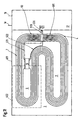
- FIG. 1 shows the plan view of a semiconductor power component 1 according to the invention with a RESURF area 4 arranged between high-voltage side 2 and low-voltage side 3.
- the high-voltage side 2 and the low-voltage side 3 of the power component 1 shown here engage in one another in a finger-shaped manner separated by the RESURF area 4.
- the illustrated power component 1 could be, for example, a diode, a LIGBT, an LDMOS or even a bipolar transistor.
- a poly-silicon resistor 5-here even four poly-silicon resistors 5- is arranged above the RESURF region 4.
- the poly-silicon resistors 5 are guided meander-shaped within the finger structure of the RESURF region 4 from the high-voltage side 2 to the low-voltage side 3.
- the poly-silicon resistors 5 are electrically isolated from the RESURF region 4, which is illustrated by FIGS. 3 to 6.
- the four poly-silicon resistors 5 are propagated at equal intervals one after the other from the high-voltage side 2 and open in the low-voltage side 3. It is advantageous if the poly-silicon resistors 5 have the minimum possible with regard to the manufacturing process Have width and the minimum possible distance from each other or from turn to turn and the high voltage side 2 rotate as often as possible on the basis of the design rules just mentioned.
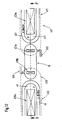
- poly-silicon resistors 5 are each in the form of a zigzag meander whose ends 8 are located on the low-voltage side 3 and whose beginnings 8 * lie on the high-voltage side 2.
- zigzag meandering poly-silicon resistors 5 a signal transfer between the high voltage side 2 and low voltage side 3 is possible.
- the outer corners 6 of the zigzag meanders are respectively connected to poly-silicon strips 7. These poly-silicon strips 7 run on tracks of approximately constant distance from the high-voltage side 2 and the low-voltage side 3, meandering along the RESURF region 4.
- the poly-silicon resistor is designed as a single zigzag meander having two outer ends. These can be completed in the manner described by poly-silicon strips.
- the poly-silicon resistor consists of a parallel connection of the above-described multiple zigzag meanders. The parallel connection is obtained by pairwise connecting the originally adjacent inner ends of the plurality of zigzag meanders.
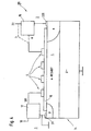
- the lateral pnp transistor 10 shown in cross-section in FIG. 3 has the connections BASE 11, EMITTER 120 and COLLECTOR 13. Such a transistor may comprise any number of fingers and be fabricated on p - substrate, p - / p + substrate or SOI substrate. The variant on p - substrate 14 is shown in detail here. In each of these cases, the RESURF region 4 is then n-doped. The poly-silicon resistor 5 arranged above the RESURF region 4 is electrically insulated from the RESURF region 4 by a field oxide layer 15.
- the poly-silicon resistor 5 is used for signal transmission between a lying at the potential of the high voltage side 2 sensing circuit 16 and a lying on the potential of the low voltage side 3 drive and evaluation circuit 17.
- the poly-silicon resistor 5 is on the High voltage side 2, namely the emitter side, subjected to a voltage signal in the order of the emitter voltage, what it can be connected directly to the external emitter terminal 12 of the sensing circuit 16 alternatively, which is indicated by the wiring b, or with the sensing circuit 16, which by the Wiring a is indicated.
- the low voltage side, ie the collector side, of the poly-silicon resistor 5 is connected via a signal detection input 101 to the drive and evaluation circuit 17.
- the drive and evaluation circuit 17 also has an optional status output 18 and a drive input 19.
- the bipolar transistor 10 shown here can be controlled via the drive input 19 from an external signal source.
- the base terminal 11 can be controlled directly by the drive and evaluation circuit 17.
- the drive and evaluation circuit 17 comprises a drive output 201 with a high-voltage-resistant switching element. This may be, for example, an npn or NMOS transistor whose emitter or source is connected to ground potential and whose collector or drain is connected to the base terminal 11.
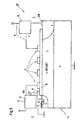
- Fig. 4 shows a to Figure 3 analogous cross-sectional view of a lateral diode 20 to the terminals anode 21 and the cathode 220.
- the diode 20 may have any number of fingers and, like the one shown in Figure 3 pnp transistor on p -.. - substrate , p - / p + substrate or on SOI substrate.
- the variant on p - substrate 14 is shown in detail here. In these three cases, the RESURF region 4 always has an n-type doping.
- the poly-silicon resistor 5 is again electrically insulated from the semiconductor substrate 14 by a field oxide layer 15.
- the poly-silicon resistor 5 also serves here again for signal transmission between a sensor circuit 16 located at the potential of the high-voltage side 2 and a drive and evaluation circuit 17 located at the potential of the low-voltage side 3.
- the sensor circuit 16 has an external cathode connection 22 for connection a burden.
- On the high voltage side 2 of the poly-silicon resistor 5 may alternatively be connected directly to this external cathode terminal 22, which is indicated by the wiring b, or with the sensing circuit 16, which is indicated by the wiring a.
- the drive and evaluation circuit 17 has a status input 18 and a signal detection input 101, via which the poly-silicon resistor 5 is connected to the drive and evaluation circuit 17.
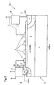
- Fig. 5 is a view similar to Figures 3 and 4 cross-sectional view of an LDMOS 30 having the terminals GATE 31, SOURCE 32 and drain 330. Also, such a LDMOS can have as many fingers and how the components previously described on p - - substrate p - / p + - be prepared substrate or SOI substrate. Shown in detail here is the variant on p - - substrate 14.
- An Trust- and Evaluation circuit 17 is electrically insulated by a field oxide layer 15 against the semiconductor substrate 14.
- the drive and evaluation circuit 17 On the high voltage side, it can alternatively be connected directly to the external drain connection 33 (wiring b) or to the sensing circuit 16 (wiring a).
- Low-voltage side of the poly-silicon resistor 5 is connected to a signal detection input 101 of the drive and evaluation circuit 17.
- the drive and evaluation circuit 17 also has an optional status output 18 and a drive input 19, via which the LDMOS 30 can be controlled from an external signal source.
- the drive and evaluation circuit 17 comprises a drive output 201, which is connected to the GATE 31.
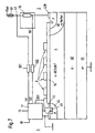
- FIG. 6 shows a cross-section similar to FIGS. 3 to 5 through a LIGBT 40 with the connections GATE 41, ANODE 420 and cathode 43.
- a LIGBT can also have any number of fingers and can be mounted on p - - substrate, p / p + - Substrate or SOI substrate to be produced, wherein the RESURF region 4 always has an n-type doping.
- the variant on p - substrate 14 is shown in detail here.
- the poly-silicon resistor 5 is electrically insulated from the semiconductor substrate 14 by a field oxide layer 15.
- the poly-silicon resistor 5 may alternatively be connected directly to the external anode terminal 42 (line routing b) or to the sensing circuit 16 (FIG. Wiring a) be connected.
- Low-voltage side of the poly-silicon resistor 5 is connected to a signal detection input 101 of the drive and evaluation circuit 17.
- the drive and evaluation circuit 17 also has an optional status output 18 and a Control input 19, via which the LIGBT 40 can be controlled from an external signal source.
- the drive and evaluation circuit 17 comprises a drive output 201, which is connected to the GATE 41, so that the drive and evaluation circuit 17 can selectively act on the GATE 41.
- the sense circuit 16 and the drive and evaluation circuit 17 could be used, for example, to detect and limit the anode voltage of the LIGBT.
- the signal guide b has been selected, so that the sensor circuit 16 can be replaced by a conductive connection.
- To the external anode terminal 42 is connected an inductive load through which a current flows; the LIGBT is on. If the LIGBT is now switched off due to a control signal at the control input 19, for which purpose the drive output 201 of the drive and evaluation circuit 17 reduces its voltage to values below the threshold voltage of the LIGBT, then the voltage at the anode connection 420 or 42 increases. This increase would produce such high anode voltages without further action that the semiconductor device reaches its breakdown voltage.
- the voltage increase at anode terminal 420 or 42 is transmitted via the meandering poly-silicon resistor 5 as a current or voltage signal to the low-voltage side 3 and the signal detection input 101 of the drive and evaluation circuit 17 is supplied.
- the drive and evaluation circuit 17 compares this signal with a reference value, upon reaching the gate 41 is controlled via the drive output 201 such that the anode voltage is limited to a predetermined value.
- LVIGBT lateral-vertical IGBT
- the LVIGBT shown in Fig. 7 is made on a p - / p + substrate but otherwise has the same structure as the LIGBT shown in Fig. 6, so that like reference numerals in Figs. 6 and 7 also denote like elements and circuit components describe.
- the external anode terminal 42 of the LVIGBT is here connected to an inductive load 60, which is fed by an operating voltage source Vbat.
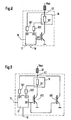
- a sense circuit 16 is used in the embodiment shown here, a resistor 16, which may be implemented, for example in the form of a poly-silicon resistor.
- the drive and evaluation circuit 17 If the drive and evaluation circuit 17 is supplied with a drive voltage via the drive input 19, then the drive output 201 and thus the gate 41 assumes a positive voltage;
- the LVIGBT is turned on: On the surface of the semiconductor under the gate 41, in particular in the p-region 44, an inversion channel is generated, after which electrons are injected from the n-region 45 into the resurf region 4. Thereupon the p-anode 47 responds with a hole injection. As a result, the resurf region 4 and large parts of the p - region 48 are flooded by charge carriers and get into the state of high injection.
- a current of Vbat now flows through the load 60, the resistor 16, via the anode metallization 420, the p-anode 47 and the n-buffer 46.
- a portion of the current flows across the p - region 48 and the p + - Area 49 to the ground on the back of the device from the other part flows through the Resurf region 4 laterally over the p-region 44 and the n-region 45 to the cathode 43, which in turn is connected to ground.
- the current does not immediately reach its static final value, but increases from zero in a slope, which depends on the height of Vbat, the magnitude of the inductance of the load 60 and the voltage drop between the external anode terminal 42 and the cathode 43 of the LVIBGT depends.
- This increase in current causes a current-proportional voltage drop across the resistor 16, which can be determined as explained below.
- the voltage applied to the resistor 16 at the external anode terminal 42 and a designated 301 point is tapped and the signal detection inputs 101 and 102 of the drive and Evaluation circuit 17 supplied.
- the voltage tap is carried out with a respective meander 501 and 502 of the poly-silicon resistor 5.
- the drive and evaluation circuit 17 forms the difference of the signals applied to the signal detection inputs 101 and 102 and thus determines a voltage proportional to the current.
- the voltage thus determined is compared in the drive and evaluation circuit 17 with two reference voltages. If the voltage determined proportional to the current reaches the value of the one reference voltage, then a status signal is generated at the status output 18 of the control and evaluation circuit.
- the drive and evaluation circuit 17 reduces the magnitude of the gate control signal at the drive output 201 to such an extent that a further increase in current through the load 60 is prevented.
- the circuit breaker shown here thus protects itself and the load 60 against overcurrents.
- FIG. 7 shows a circuit diagram of the current-limited LVIGBT just described. The structures bordered by the dashed line are integrated on a chip.
- a small part 402 of the LVIGBT is connected to the load 60 via the resistor 16. This small part 402 is then used as a sense cell. The largest part 401 of the LVIGBT is directly connected to the load 60.
- the advantage of this arrangement over the variant shown in FIG. 8 is a lower voltage drop across the power device, since only part of the load current flows through the resistor 16.
- FIGS. 10 and 11 are schematic plan views showing various possible implementations for the voltage tap across resistor 16 for the LVIGBT shown in FIG.
- the variant shown in FIG. 10 comprises two poly-silicon meanders 501 and 502, which are led directly to the resistor 16.
- the resistor 16 is also made here Poly-silicon.
- the resistor 16 remote from the ends of the poly-silicon meander 501 and 502 are connected via metal leads 510 and 520 to the signal detection inputs 101 and 102 of the drive and evaluation circuit. All other reference numerals correspond to those in Fig. 9.
- the variant shown in Fig. 11 comprises two poly-silicon zigzag meanders 501 and 502, which are guided via metal leads 511 and 522 to the resistor 16.
- the opposite ends of the poly-silicon zigzag meanders 501 and 502 are also connected via metal leads 510 and 520 to the signal detection inputs 101 and 102 of the drive and evaluation circuit. All other reference numerals correspond to those in FIG. 9.
- FIGS. 10 and 11 show a more detailed illustration of the connection guidance of the poly-silicon meanders 501 and 502 to the sense circuit 16 and to the drive and evaluation circuit 17.
- the region around the resistor 16 with the connection points shown in FIG the poly-silicon meander 501 and 502 is shown in Fig. 12 again enlarged in plan view.
- the anode metallizations 420 and 421, which cover the anode diffusions of the two LVIGBT parts 401 and 402 and parts of the resistor 16, are indicated by dashed lines.
- the anode metallization 420 contacts the p-anode diffusion 47 of the LVGBT part 402 in the region 420a and the resistor 16 in the region 420b.
- the anode metallization 421 contacts the p-anode diffusion 471 of the LVGBT part 401 in the region 421a and in the region 421b the Resistor 16.
- the p-type anode diffusions 47 and 471 are each embedded in n-type buffers 46 and 461, respectively.
- FIG. 12 illustrates that the poly-silicon meanders 501 and 502 are attached directly to the poly-silicon resistor 16 in the case shown here.
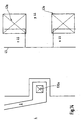
- FIG. 14 shows a plan view of a first realization option without metallization and intermediate dielectric
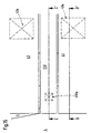
- FIG. 15 shows a plan view with metallization.
- the end of the poly-silicon meander 5 is contacted by the metal feed line 510 in such a way that it aligns with the cathode metallization 43 on the side facing the high voltage region.
- all sharp corners in the polysilicon are covered by the metallization. Both measures keep field peaks small, which can lead to a reduction of the breakdown voltage of the device.
- 510a designates the region of the metal feed line 510 which contacts the poly-silicon meander 5.
- 43a denotes the regions of the cathode metallization 43 which contact the silicon surface.
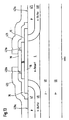
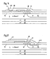
- Figures 16 and 17 show cross-sectional images taken along sections CC 'and DD' in Figure 15 without the prior art passivation layers overlying the metallizations.
- the n-type region 45 does not extend over the region over which the metal lead 510 extends, which serves to increase the latch-up strength of the device.
- the intermediate dielectric is designated 80, while the gate oxide is designated 81.
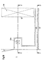
- FIG. 18 shows in plan view a further realization option with metallization and intermediate dielectric.
- the end of the poly-silicon meander 5 is contacted by the metal lead 510 such that it forms an alignment with the cathode metallization 43 on the side facing the high-voltage region.
- all sharp corners in the polysilicon are covered by the metallization. Both measures keep field peaks small, which can lead to a reduction of the breakdown voltage of the device.
- FIGS. 19 and 20 show cross-sectional images along the sections EE 'and FF' in FIG. 18 without the prior art passivation layers lying above the metallizations.
- the n-type region 45 does not extend over the region over which the metal lead 510 extends, which serves to increase the latch-up strength of the device.
- the variant illustrated in FIGS. 18 to 20 will be selected if the end of a poly-silicon meander to be contacted lies at a point which is so unfavorable in the component that the variant described in connection with FIGS. 14 to 17 can not be implemented.
- the contacting of the high-voltage side end of a poly-silicon meander can be carried out accordingly.
Landscapes
- Semiconductor Integrated Circuits (AREA)
- Metal-Oxide And Bipolar Metal-Oxide Semiconductor Integrated Circuits (AREA)
- Insulated Gate Type Field-Effect Transistor (AREA)
- Bipolar Transistors (AREA)
Applications Claiming Priority (3)
| Application Number | Priority Date | Filing Date | Title |
|---|---|---|---|
| DE10023956 | 2000-05-16 | ||
| DE10023956A DE10023956A1 (de) | 2000-05-16 | 2000-05-16 | Halbleiter-Leistungsbauelement |
| PCT/DE2001/001774 WO2001088992A2 (de) | 2000-05-16 | 2001-05-10 | Halbleiter-leistungsbauelement |
Publications (2)
| Publication Number | Publication Date |
|---|---|
| EP1284019A2 EP1284019A2 (de) | 2003-02-19 |
| EP1284019B1 true EP1284019B1 (de) | 2007-09-26 |
Family
ID=7642253
Family Applications (1)
| Application Number | Title | Priority Date | Filing Date |
|---|---|---|---|
| EP01940224A Expired - Lifetime EP1284019B1 (de) | 2000-05-16 | 2001-05-10 | Halbleiter-leistungsbauelement |
Country Status (7)
| Country | Link |
|---|---|
| US (1) | US20040046225A1 (cs) |
| EP (1) | EP1284019B1 (cs) |
| JP (1) | JP2003533886A (cs) |
| KR (1) | KR100844283B1 (cs) |
| CZ (1) | CZ302020B6 (cs) |
| DE (2) | DE10023956A1 (cs) |
| WO (1) | WO2001088992A2 (cs) |
Families Citing this family (12)
| Publication number | Priority date | Publication date | Assignee | Title |
|---|---|---|---|---|
| GB2387481B (en) | 2002-04-10 | 2005-08-31 | Intense Photonics Ltd | Integrated active photonic device and photodetector |
| DE102005037409A1 (de) | 2004-08-09 | 2006-03-30 | International Rectifier Corp., El Segundo | Start-Up Schalter um einer Anwendungsschaltung eine Start-Up Spannung zur Verfügung zu stellen |
| JP4797203B2 (ja) | 2008-12-17 | 2011-10-19 | 三菱電機株式会社 | 半導体装置 |
| JP2013120815A (ja) * | 2011-12-07 | 2013-06-17 | Sony Corp | Esd保護回路およびこれを備えた半導体装置 |
| US10396167B2 (en) | 2015-12-15 | 2019-08-27 | Fuji Electric Co., Ltd. | Semiconductor device |
| JP6597269B2 (ja) | 2015-12-15 | 2019-10-30 | 富士電機株式会社 | 半導体装置 |
| JP6690336B2 (ja) | 2016-03-18 | 2020-04-28 | 富士電機株式会社 | 半導体装置 |
| EP3327756B1 (en) * | 2016-11-24 | 2019-11-06 | Melexis Technologies NV | Die edge integrity monitoring system and corresponding method |
| DE102017130213B4 (de) * | 2017-12-15 | 2021-10-21 | Infineon Technologies Ag | Planarer feldeffekttransistor |
| DE102019119805B4 (de) * | 2018-09-28 | 2024-09-26 | Taiwan Semiconductor Manufacturing Co., Ltd. | Halbleitervorrichtung, die einen kondensator aufweist, sowie verfahren zu ihrer herstellung |
| US11152356B2 (en) * | 2019-02-19 | 2021-10-19 | Semiconductor Components Industries, Llc | Method of forming a semiconductor device and structure therefor |
| CN113948571B (zh) * | 2021-10-18 | 2023-08-25 | 上海华虹宏力半导体制造有限公司 | 半导体结构及其形成方法 |
Family Cites Families (14)
| Publication number | Priority date | Publication date | Assignee | Title |
|---|---|---|---|---|
| US4157563A (en) * | 1971-07-02 | 1979-06-05 | U.S. Philips Corporation | Semiconductor device |
| NL187415C (nl) * | 1980-09-08 | 1991-09-16 | Philips Nv | Halfgeleiderinrichting met gereduceerde oppervlakteveldsterkte. |
| JPH04245483A (ja) * | 1991-01-30 | 1992-09-02 | Nippondenso Co Ltd | 半導体装置 |
| JPH05121418A (ja) * | 1991-10-24 | 1993-05-18 | Nec Corp | 半導体装置 |
| JP3207615B2 (ja) * | 1992-06-24 | 2001-09-10 | 株式会社東芝 | 半導体装置 |
| KR0127003Y1 (ko) * | 1992-06-24 | 1998-12-01 | 사또 후미오 | 전력 반도체 집적 회로 장치 |
| JP3123309B2 (ja) * | 1993-08-18 | 2001-01-09 | 富士電機株式会社 | センサ素子付き半導体装置 |
| US5486718A (en) * | 1994-07-05 | 1996-01-23 | Motorola, Inc. | High voltage planar edge termination structure and method of making same |
| GB9423423D0 (en) * | 1994-11-14 | 1995-01-11 | Fuji Electric Co Ltd | Semiconductor device |
| JPH08241959A (ja) * | 1995-03-02 | 1996-09-17 | Toshiba Corp | 半導体装置 |
| DE19538090A1 (de) * | 1995-10-13 | 1997-04-17 | Asea Brown Boveri | Leistungshalbleiterelement |
| EP0866557A1 (en) * | 1997-03-18 | 1998-09-23 | Carlo Gavazzi AG | Solid state relay |
| JP3905981B2 (ja) * | 1998-06-30 | 2007-04-18 | 株式会社東芝 | 高耐圧半導体装置 |
| US6603185B1 (en) * | 1999-02-01 | 2003-08-05 | Fuji Electric Co., Ltd. | Voltage withstanding structure for a semiconductor device |
-
2000
- 2000-05-16 DE DE10023956A patent/DE10023956A1/de not_active Ceased
-
2001
- 2001-05-10 WO PCT/DE2001/001774 patent/WO2001088992A2/de not_active Ceased
- 2001-05-10 JP JP2001584492A patent/JP2003533886A/ja active Pending
- 2001-05-10 KR KR1020027015260A patent/KR100844283B1/ko not_active Expired - Fee Related
- 2001-05-10 US US10/276,568 patent/US20040046225A1/en not_active Abandoned
- 2001-05-10 DE DE50113060T patent/DE50113060D1/de not_active Expired - Lifetime
- 2001-05-10 CZ CZ20023761A patent/CZ302020B6/cs not_active IP Right Cessation
- 2001-05-10 EP EP01940224A patent/EP1284019B1/de not_active Expired - Lifetime
Non-Patent Citations (1)
| Title |
|---|
| None * |
Also Published As
| Publication number | Publication date |
|---|---|
| US20040046225A1 (en) | 2004-03-11 |
| EP1284019A2 (de) | 2003-02-19 |
| JP2003533886A (ja) | 2003-11-11 |
| WO2001088992A3 (de) | 2002-05-30 |
| DE10023956A1 (de) | 2001-11-22 |
| WO2001088992A2 (de) | 2001-11-22 |
| KR100844283B1 (ko) | 2008-07-09 |
| CZ302020B6 (cs) | 2010-09-08 |
| KR20030019380A (ko) | 2003-03-06 |
| CZ20023761A3 (cs) | 2003-05-14 |
| DE50113060D1 (de) | 2007-11-08 |
Similar Documents
| Publication | Publication Date | Title |
|---|---|---|
| DE19704995B4 (de) | Integrierte Hochspannungs-Leistungsschaltung | |
| EP1019964B1 (de) | Integrierte halbleiterschaltung mit schutzstruktur zum schutz vor elektrostatischer entladung | |
| DE10322593B4 (de) | Halbleiterbauteil und dieses verwendender integrierter Schaltkreis | |
| DE19811297B4 (de) | MOS-Halbleitervorrichtung mit hoher Durchbruchspannung | |
| DE102014110366B4 (de) | Mos-leistungstransistor mit integriertem gatewiderstand | |
| DE69212868T2 (de) | Halbleiterbauelement mit n-dotiertem Gebiet niedriger Konzentration zur Verbesserung der dV/dt Eigenschaften | |
| EP1175700B1 (de) | Halbleiter-bauelement | |
| DE69305909T2 (de) | Leistungsanordnung mit isoliertem Gate-Kontakt-Gebiet | |
| DE3834841C2 (de) | Integrierte Anordnung in einem Substrat zur Vermeidung parasitärer Substrateffekte | |
| DE69330455T2 (de) | Überspannungsschutzstruktur für vertikale Halbleiterkomponenten | |
| DE102009037487A1 (de) | Halbleitervorrichtung | |
| DE19914697A1 (de) | Verarmungs-MOS-Halbleiterbauelement und MOS-Leistungs-IC | |
| DE69329097T2 (de) | Neue Anordnung für eine Vorrichtung mit vielen HV-LDMOS Transistoren und einer Schaltung innerhalb einer schwebenden Wanne | |
| EP1284019B1 (de) | Halbleiter-leistungsbauelement | |
| DE102004045467B4 (de) | Feldeffekt-Trenchtransistor | |
| DE102012111910A1 (de) | Halbleitervorrichtung, die ein erstes und ein zweites Halbleiterelement aufweist | |
| WO1993000709A1 (de) | Monolithisch integrierte schaltungsanordnung | |
| EP1412973B1 (de) | Halbleiterstruktur mit feldplatte | |
| EP1870938A1 (de) | Halbleiterschutzstruktur für eine elektrostatische Entladung | |
| DE10243743B4 (de) | Quasivertikales Halbleiterbauelement | |
| DE19902749C2 (de) | Leistungstransistoranordnung mit hoher Spannungsfestigkeit | |
| DE69418109T2 (de) | Aus einem Bipolartransistor und einem Feldeffekt-Transistor bestehende integrierte Anordnung | |
| EP1135806A1 (de) | Steuerbares halbleiterbauelement mit einem gatevorwiderstand | |
| DE10123818B4 (de) | Anordnung mit Schutzfunktion für ein Halbleiterbauelement | |
| EP1297574B1 (de) | Schutzvorrichtung gegen elektrostatische entladungen |
Legal Events
| Date | Code | Title | Description |
|---|---|---|---|
| PUAI | Public reference made under article 153(3) epc to a published international application that has entered the european phase |
Free format text: ORIGINAL CODE: 0009012 |
|
| 17P | Request for examination filed |
Effective date: 20021216 |
|
| AK | Designated contracting states |
Designated state(s): AT BE CH CY DE DK ES FI FR GB GR IE IT LI LU MC NL PT SE TR |
|
| RBV | Designated contracting states (corrected) |
Designated state(s): DE FR GB IT |
|
| GRAP | Despatch of communication of intention to grant a patent |
Free format text: ORIGINAL CODE: EPIDOSNIGR1 |
|
| GRAS | Grant fee paid |
Free format text: ORIGINAL CODE: EPIDOSNIGR3 |
|
| GRAA | (expected) grant |
Free format text: ORIGINAL CODE: 0009210 |
|
| AK | Designated contracting states |
Kind code of ref document: B1 Designated state(s): DE FR GB IT |
|
| REG | Reference to a national code |
Ref country code: GB Ref legal event code: FG4D Free format text: NOT ENGLISH |
|
| REF | Corresponds to: |
Ref document number: 50113060 Country of ref document: DE Date of ref document: 20071108 Kind code of ref document: P |
|
| GBT | Gb: translation of ep patent filed (gb section 77(6)(a)/1977) |
Effective date: 20080110 |
|
| ET | Fr: translation filed | ||
| PLBE | No opposition filed within time limit |
Free format text: ORIGINAL CODE: 0009261 |
|
| STAA | Information on the status of an ep patent application or granted ep patent |
Free format text: STATUS: NO OPPOSITION FILED WITHIN TIME LIMIT |
|
| 26N | No opposition filed |
Effective date: 20080627 |
|
| PGFP | Annual fee paid to national office [announced via postgrant information from national office to epo] |
Ref country code: GB Payment date: 20130522 Year of fee payment: 13 |
|
| REG | Reference to a national code |
Ref country code: DE Ref legal event code: R084 Ref document number: 50113060 Country of ref document: DE |
|
| REG | Reference to a national code |
Ref country code: DE Ref legal event code: R084 Ref document number: 50113060 Country of ref document: DE Effective date: 20140905 |
|
| GBPC | Gb: european patent ceased through non-payment of renewal fee |
Effective date: 20140510 |
|
| REG | Reference to a national code |
Ref country code: FR Ref legal event code: PLFP Year of fee payment: 15 |
|
| PG25 | Lapsed in a contracting state [announced via postgrant information from national office to epo] |
Ref country code: GB Free format text: LAPSE BECAUSE OF NON-PAYMENT OF DUE FEES Effective date: 20140510 |
|
| PGFP | Annual fee paid to national office [announced via postgrant information from national office to epo] |
Ref country code: IT Payment date: 20150519 Year of fee payment: 15 Ref country code: FR Payment date: 20150519 Year of fee payment: 15 |
|
| PGFP | Annual fee paid to national office [announced via postgrant information from national office to epo] |
Ref country code: DE Payment date: 20160726 Year of fee payment: 16 |
|
| PG25 | Lapsed in a contracting state [announced via postgrant information from national office to epo] |
Ref country code: IT Free format text: LAPSE BECAUSE OF NON-PAYMENT OF DUE FEES Effective date: 20160510 |
|
| REG | Reference to a national code |
Ref country code: FR Ref legal event code: ST Effective date: 20170131 |
|
| PG25 | Lapsed in a contracting state [announced via postgrant information from national office to epo] |
Ref country code: FR Free format text: LAPSE BECAUSE OF NON-PAYMENT OF DUE FEES Effective date: 20160531 |
|
| REG | Reference to a national code |
Ref country code: DE Ref legal event code: R119 Ref document number: 50113060 Country of ref document: DE |
|
| PG25 | Lapsed in a contracting state [announced via postgrant information from national office to epo] |
Ref country code: DE Free format text: LAPSE BECAUSE OF NON-PAYMENT OF DUE FEES Effective date: 20171201 |