EP1284433A2 - Dispositif d'affichage transflectif à cristaux liquides et son procédé de fabrication - Google Patents
Dispositif d'affichage transflectif à cristaux liquides et son procédé de fabrication Download PDFInfo
- Publication number
- EP1284433A2 EP1284433A2 EP02017478A EP02017478A EP1284433A2 EP 1284433 A2 EP1284433 A2 EP 1284433A2 EP 02017478 A EP02017478 A EP 02017478A EP 02017478 A EP02017478 A EP 02017478A EP 1284433 A2 EP1284433 A2 EP 1284433A2
- Authority
- EP
- European Patent Office
- Prior art keywords
- electrode film
- film
- reflection
- substrate
- transflective type
- Prior art date
- Legal status (The legal status is an assumption and is not a legal conclusion. Google has not performed a legal analysis and makes no representation as to the accuracy of the status listed.)
- Withdrawn
Links
- 239000004973 liquid crystal related substance Substances 0.000 title claims description 56
- 238000000034 method Methods 0.000 title claims description 44
- 238000004519 manufacturing process Methods 0.000 title claims description 42
- 239000000758 substrate Substances 0.000 claims abstract description 109
- 230000005540 biological transmission Effects 0.000 claims abstract description 87
- 239000011159 matrix material Substances 0.000 claims abstract description 36
- 230000001788 irregular Effects 0.000 claims abstract description 34
- 239000002184 metal Substances 0.000 claims description 36
- 229910052751 metal Inorganic materials 0.000 claims description 36
- 238000006243 chemical reaction Methods 0.000 claims description 35
- 230000004888 barrier function Effects 0.000 claims description 19
- 238000002161 passivation Methods 0.000 claims description 18
- 230000010287 polarization Effects 0.000 claims description 12
- 239000003513 alkali Substances 0.000 claims description 11
- 238000000151 deposition Methods 0.000 claims description 10
- 238000010276 construction Methods 0.000 claims description 9
- 238000005406 washing Methods 0.000 claims description 8
- 238000011049 filling Methods 0.000 claims description 6
- 239000004020 conductor Substances 0.000 claims description 5
- 238000005530 etching Methods 0.000 claims description 5
- 239000000463 material Substances 0.000 claims description 5
- 230000015572 biosynthetic process Effects 0.000 claims description 4
- 238000010438 heat treatment Methods 0.000 claims description 4
- 230000003628 erosive effect Effects 0.000 abstract description 29
- 239000000126 substance Substances 0.000 abstract description 11
- 239000010408 film Substances 0.000 description 304
- 238000009413 insulation Methods 0.000 description 31
- 230000003287 optical effect Effects 0.000 description 12
- 239000004925 Acrylic resin Substances 0.000 description 9
- 229920000178 Acrylic resin Polymers 0.000 description 9
- 229910052750 molybdenum Inorganic materials 0.000 description 9
- 238000004544 sputter deposition Methods 0.000 description 9
- 238000010586 diagram Methods 0.000 description 8
- 229920002120 photoresistant polymer Polymers 0.000 description 6
- 238000009825 accumulation Methods 0.000 description 5
- 230000000694 effects Effects 0.000 description 5
- 239000004065 semiconductor Substances 0.000 description 5
- 238000003860 storage Methods 0.000 description 5
- NIXOWILDQLNWCW-UHFFFAOYSA-N acrylic acid group Chemical group C(C=C)(=O)O NIXOWILDQLNWCW-UHFFFAOYSA-N 0.000 description 4
- 230000007246 mechanism Effects 0.000 description 4
- 230000007547 defect Effects 0.000 description 3
- 230000002950 deficient Effects 0.000 description 3
- 238000000206 photolithography Methods 0.000 description 3
- 239000004988 Nematic liquid crystal Substances 0.000 description 2
- 229910004205 SiNX Inorganic materials 0.000 description 2
- VYPSYNLAJGMNEJ-UHFFFAOYSA-N Silicium dioxide Chemical compound O=[Si]=O VYPSYNLAJGMNEJ-UHFFFAOYSA-N 0.000 description 2
- 101100214491 Solanum lycopersicum TFT3 gene Proteins 0.000 description 2
- 230000002159 abnormal effect Effects 0.000 description 2
- 230000008859 change Effects 0.000 description 2
- 239000013078 crystal Substances 0.000 description 2
- 230000003247 decreasing effect Effects 0.000 description 2
- 238000005516 engineering process Methods 0.000 description 2
- 238000002474 experimental method Methods 0.000 description 2
- 239000011521 glass Substances 0.000 description 2
- 230000000670 limiting effect Effects 0.000 description 2
- 229920000642 polymer Polymers 0.000 description 2
- 230000008569 process Effects 0.000 description 2
- 238000002310 reflectometry Methods 0.000 description 2
- 238000002791 soaking Methods 0.000 description 2
- 239000010409 thin film Substances 0.000 description 2
- 241000872198 Serjania polyphylla Species 0.000 description 1
- 229910021417 amorphous silicon Inorganic materials 0.000 description 1
- QVGXLLKOCUKJST-UHFFFAOYSA-N atomic oxygen Chemical compound [O] QVGXLLKOCUKJST-UHFFFAOYSA-N 0.000 description 1
- 230000002238 attenuated effect Effects 0.000 description 1
- 230000000903 blocking effect Effects 0.000 description 1
- 229910052804 chromium Inorganic materials 0.000 description 1
- 238000004140 cleaning Methods 0.000 description 1
- 229910052681 coesite Inorganic materials 0.000 description 1
- 230000001276 controlling effect Effects 0.000 description 1
- 229910052906 cristobalite Inorganic materials 0.000 description 1
- 230000007423 decrease Effects 0.000 description 1
- 230000002542 deteriorative effect Effects 0.000 description 1
- 230000005684 electric field Effects 0.000 description 1
- 239000012535 impurity Substances 0.000 description 1
- PJXISJQVUVHSOJ-UHFFFAOYSA-N indium(III) oxide Inorganic materials [O-2].[O-2].[O-2].[In+3].[In+3] PJXISJQVUVHSOJ-UHFFFAOYSA-N 0.000 description 1
- 238000007254 oxidation reaction Methods 0.000 description 1
- 230000001590 oxidative effect Effects 0.000 description 1
- 229910052760 oxygen Inorganic materials 0.000 description 1
- 239000001301 oxygen Substances 0.000 description 1
- 230000036961 partial effect Effects 0.000 description 1
- 238000000059 patterning Methods 0.000 description 1
- 238000000623 plasma-assisted chemical vapour deposition Methods 0.000 description 1
- 230000001737 promoting effect Effects 0.000 description 1
- 230000009467 reduction Effects 0.000 description 1
- 230000002829 reductive effect Effects 0.000 description 1
- 230000001105 regulatory effect Effects 0.000 description 1
- 238000007789 sealing Methods 0.000 description 1
- 239000000377 silicon dioxide Substances 0.000 description 1
- 229910052814 silicon oxide Inorganic materials 0.000 description 1
- 238000004528 spin coating Methods 0.000 description 1
- 229910052682 stishovite Inorganic materials 0.000 description 1
- 229910052719 titanium Inorganic materials 0.000 description 1
- 229910052905 tridymite Inorganic materials 0.000 description 1
- 229910052721 tungsten Inorganic materials 0.000 description 1
- XLYOFNOQVPJJNP-UHFFFAOYSA-N water Substances O XLYOFNOQVPJJNP-UHFFFAOYSA-N 0.000 description 1
Images






Classifications
-
- G—PHYSICS
- G02—OPTICS
- G02F—OPTICAL DEVICES OR ARRANGEMENTS FOR THE CONTROL OF LIGHT BY MODIFICATION OF THE OPTICAL PROPERTIES OF THE MEDIA OF THE ELEMENTS INVOLVED THEREIN; NON-LINEAR OPTICS; FREQUENCY-CHANGING OF LIGHT; OPTICAL LOGIC ELEMENTS; OPTICAL ANALOGUE/DIGITAL CONVERTERS
- G02F1/00—Devices or arrangements for the control of the intensity, colour, phase, polarisation or direction of light arriving from an independent light source, e.g. switching, gating or modulating; Non-linear optics
- G02F1/01—Devices or arrangements for the control of the intensity, colour, phase, polarisation or direction of light arriving from an independent light source, e.g. switching, gating or modulating; Non-linear optics for the control of the intensity, phase, polarisation or colour
- G02F1/13—Devices or arrangements for the control of the intensity, colour, phase, polarisation or direction of light arriving from an independent light source, e.g. switching, gating or modulating; Non-linear optics for the control of the intensity, phase, polarisation or colour based on liquid crystals, e.g. single liquid crystal display cells
- G02F1/133—Constructional arrangements; Operation of liquid crystal cells; Circuit arrangements
- G02F1/1333—Constructional arrangements; Manufacturing methods
- G02F1/1335—Structural association of cells with optical devices, e.g. polarisers or reflectors
- G02F1/133553—Reflecting elements
- G02F1/133555—Transflectors
-
- A—HUMAN NECESSITIES
- A47—FURNITURE; DOMESTIC ARTICLES OR APPLIANCES; COFFEE MILLS; SPICE MILLS; SUCTION CLEANERS IN GENERAL
- A47J—KITCHEN EQUIPMENT; COFFEE MILLS; SPICE MILLS; APPARATUS FOR MAKING BEVERAGES
- A47J37/00—Baking; Roasting; Grilling; Frying
- A47J37/04—Roasting apparatus with movably-mounted food supports or with movable heating implements; Spits
- A47J37/045—Roasting apparatus with movably-mounted food supports or with movable heating implements; Spits with endless conveyors
-
- A—HUMAN NECESSITIES
- A47—FURNITURE; DOMESTIC ARTICLES OR APPLIANCES; COFFEE MILLS; SPICE MILLS; SUCTION CLEANERS IN GENERAL
- A47J—KITCHEN EQUIPMENT; COFFEE MILLS; SPICE MILLS; APPARATUS FOR MAKING BEVERAGES
- A47J37/00—Baking; Roasting; Grilling; Frying
- A47J37/06—Roasters; Grills; Sandwich grills
- A47J37/07—Roasting devices for outdoor use; Barbecues
- A47J37/0786—Accessories
- A47J2037/0795—Adjustable food supports, e.g. for height adjustment
-
- A—HUMAN NECESSITIES
- A47—FURNITURE; DOMESTIC ARTICLES OR APPLIANCES; COFFEE MILLS; SPICE MILLS; SUCTION CLEANERS IN GENERAL
- A47J—KITCHEN EQUIPMENT; COFFEE MILLS; SPICE MILLS; APPARATUS FOR MAKING BEVERAGES
- A47J37/00—Baking; Roasting; Grilling; Frying
- A47J37/04—Roasting apparatus with movably-mounted food supports or with movable heating implements; Spits
- A47J37/041—Roasting apparatus with movably-mounted food supports or with movable heating implements; Spits with food supports rotating about a horizontal axis
-
- A—HUMAN NECESSITIES
- A47—FURNITURE; DOMESTIC ARTICLES OR APPLIANCES; COFFEE MILLS; SPICE MILLS; SUCTION CLEANERS IN GENERAL
- A47J—KITCHEN EQUIPMENT; COFFEE MILLS; SPICE MILLS; APPARATUS FOR MAKING BEVERAGES
- A47J37/00—Baking; Roasting; Grilling; Frying
- A47J37/06—Roasters; Grills; Sandwich grills
- A47J37/07—Roasting devices for outdoor use; Barbecues
- A47J37/0745—Roasting devices for outdoor use; Barbecues with motor-driven food supports
-
- A—HUMAN NECESSITIES
- A47—FURNITURE; DOMESTIC ARTICLES OR APPLIANCES; COFFEE MILLS; SPICE MILLS; SUCTION CLEANERS IN GENERAL
- A47J—KITCHEN EQUIPMENT; COFFEE MILLS; SPICE MILLS; APPARATUS FOR MAKING BEVERAGES
- A47J37/00—Baking; Roasting; Grilling; Frying
- A47J37/06—Roasters; Grills; Sandwich grills
- A47J37/07—Roasting devices for outdoor use; Barbecues
- A47J37/0786—Accessories
-
- G—PHYSICS
- G02—OPTICS
- G02F—OPTICAL DEVICES OR ARRANGEMENTS FOR THE CONTROL OF LIGHT BY MODIFICATION OF THE OPTICAL PROPERTIES OF THE MEDIA OF THE ELEMENTS INVOLVED THEREIN; NON-LINEAR OPTICS; FREQUENCY-CHANGING OF LIGHT; OPTICAL LOGIC ELEMENTS; OPTICAL ANALOGUE/DIGITAL CONVERTERS
- G02F1/00—Devices or arrangements for the control of the intensity, colour, phase, polarisation or direction of light arriving from an independent light source, e.g. switching, gating or modulating; Non-linear optics
- G02F1/01—Devices or arrangements for the control of the intensity, colour, phase, polarisation or direction of light arriving from an independent light source, e.g. switching, gating or modulating; Non-linear optics for the control of the intensity, phase, polarisation or colour
- G02F1/13—Devices or arrangements for the control of the intensity, colour, phase, polarisation or direction of light arriving from an independent light source, e.g. switching, gating or modulating; Non-linear optics for the control of the intensity, phase, polarisation or colour based on liquid crystals, e.g. single liquid crystal display cells
- G02F1/133—Constructional arrangements; Operation of liquid crystal cells; Circuit arrangements
- G02F1/1333—Constructional arrangements; Manufacturing methods
- G02F1/1335—Structural association of cells with optical devices, e.g. polarisers or reflectors
- G02F1/133504—Diffusing, scattering, diffracting elements
-
- G—PHYSICS
- G02—OPTICS
- G02F—OPTICAL DEVICES OR ARRANGEMENTS FOR THE CONTROL OF LIGHT BY MODIFICATION OF THE OPTICAL PROPERTIES OF THE MEDIA OF THE ELEMENTS INVOLVED THEREIN; NON-LINEAR OPTICS; FREQUENCY-CHANGING OF LIGHT; OPTICAL LOGIC ELEMENTS; OPTICAL ANALOGUE/DIGITAL CONVERTERS
- G02F1/00—Devices or arrangements for the control of the intensity, colour, phase, polarisation or direction of light arriving from an independent light source, e.g. switching, gating or modulating; Non-linear optics
- G02F1/01—Devices or arrangements for the control of the intensity, colour, phase, polarisation or direction of light arriving from an independent light source, e.g. switching, gating or modulating; Non-linear optics for the control of the intensity, phase, polarisation or colour
- G02F1/13—Devices or arrangements for the control of the intensity, colour, phase, polarisation or direction of light arriving from an independent light source, e.g. switching, gating or modulating; Non-linear optics for the control of the intensity, phase, polarisation or colour based on liquid crystals, e.g. single liquid crystal display cells
- G02F1/133—Constructional arrangements; Operation of liquid crystal cells; Circuit arrangements
- G02F1/136—Liquid crystal cells structurally associated with a semi-conducting layer or substrate, e.g. cells forming part of an integrated circuit
- G02F1/1362—Active matrix addressed cells
- G02F1/136227—Through-hole connection of the pixel electrode to the active element through an insulation layer
-
- G—PHYSICS
- G02—OPTICS
- G02F—OPTICAL DEVICES OR ARRANGEMENTS FOR THE CONTROL OF LIGHT BY MODIFICATION OF THE OPTICAL PROPERTIES OF THE MEDIA OF THE ELEMENTS INVOLVED THEREIN; NON-LINEAR OPTICS; FREQUENCY-CHANGING OF LIGHT; OPTICAL LOGIC ELEMENTS; OPTICAL ANALOGUE/DIGITAL CONVERTERS
- G02F1/00—Devices or arrangements for the control of the intensity, colour, phase, polarisation or direction of light arriving from an independent light source, e.g. switching, gating or modulating; Non-linear optics
- G02F1/01—Devices or arrangements for the control of the intensity, colour, phase, polarisation or direction of light arriving from an independent light source, e.g. switching, gating or modulating; Non-linear optics for the control of the intensity, phase, polarisation or colour
- G02F1/13—Devices or arrangements for the control of the intensity, colour, phase, polarisation or direction of light arriving from an independent light source, e.g. switching, gating or modulating; Non-linear optics for the control of the intensity, phase, polarisation or colour based on liquid crystals, e.g. single liquid crystal display cells
- G02F1/133—Constructional arrangements; Operation of liquid crystal cells; Circuit arrangements
- G02F1/136—Liquid crystal cells structurally associated with a semi-conducting layer or substrate, e.g. cells forming part of an integrated circuit
- G02F1/1362—Active matrix addressed cells
- G02F1/136231—Active matrix addressed cells for reducing the number of lithographic steps
- G02F1/136236—Active matrix addressed cells for reducing the number of lithographic steps using a grey or half tone lithographic process
Definitions
- the present invention relates to a Liquid Crystal Display (LCD) and method for manufacturing the same and, more particularly to, a transflective active-matrix type LCD having a transmission region and a reflection region in its pixel and method for manufacturing the same.
- LCD Liquid Crystal Display
- an LCD Because of its features of a small and thin geometry and low power consumption, an LCD has been put to practical use in a variety of applications such as an OA apparatus and a portable apparatus.
- the LCDs are classified in a transmission type and a reflection type, the LCD of the transmission type of which has no function to emit light for itself unlike a CRT or an EL display and so is provided with a back-light source separately so that display may be controlled by transmitting/blocking the back-light of liquid crystal thereof.
- the transmission type LCD can use back-light to obtain bright display independently of the surrounding environments
- a back-light source thereof typically has large power consumption of substantially a half of the total consumption thereof, thus contributing to an increase in the overall power consumption. If the LCD is driven by a battery in particular, its operating time is decreased, while if a large sized battery is mounted thereto on the other hand, its total weight is increased, thus preventing improvements in size and weight thereof.
- a reflection type LCD which utilizes surrounding light for display.
- the reflection type LCD employs a reflecting plate in place of the back-light source to transmit/block the surrounding light reflected by the reflecting plate in order to control display, so that it need not have a back-light source, to thereby reduce its power consumption, size, and weight; at the same time, however, it is largely deteriorated in visibility problematically if the surroundings are dark.
- Japanese Patent Application (KOKOKU) Laid-Open No. Hei 11-101992 discloses a transflective type LCD which can suppress power consumption of its back-light source and secure visibility independently of the surrounding environments, in which a transmission region and reflection region are provided in each pixel thereof to enable providing transmission mode display and reflection mode display on a single liquid crystal panel.
- FIG. 18 is a cross sectional view of conventional transflective type LCD.
- the conventional transflective type LCD comprises an active matrix substrate 12 on which a switching element such as a Thin Film Transistor (hereinafter abbreviated as TFT) 3 is formed, an opposing substrate 16 on which a color filter, a black matrix, etc. are formed, a liquid crystal layer 17 sandwiched by these substrates, and a back-light source 18 arranged below the active matrix substrate 12.
- a switching element such as a Thin Film Transistor (hereinafter abbreviated as TFT) 3 is formed
- an opposing substrate 16 on which a color filter, a black matrix, etc. are formed
- a liquid crystal layer 17 sandwiched by these substrates
- a back-light source 18 arranged below the active matrix substrate 12.
- each pixel is divided into a transmission region which transmits back-light and a reflection region which reflects surrounding light in such a construction that the transmission region has a transparent electrode film 5 formed on a passivation film 10 and the reflection region has a reflection electrode film 6 made of metal on an irregular film 11 made of an organic substance.
- a polarization state of the emitted light has been adjusted so as to equalize the optical path lengths of the liquid crystal layer 17 in these two regions to each other by forming the organic irregular film 11 in the reflection region thicker than that in the other so that the gap of the liquid crystal layer 17 in the reflection region may be substantially a half of that in the transmission region.
- the gradation-luminance characteristics of the liquid crystal panels need to be the same in the transmission region and the reflection regions so that an image impression in the transmission mode may match that in the reflection mode.
- the voltage-luminance characteristics (V-T) of the panel in the transmission mode may agree with those in the reflection mode.
- a gap of the liquid crystal layer 17 is different in the reflection region and the transmission region, that is, the gap with respect to the electrode is different on the side of the active matrix substrate 12 and on the side of the opposing substrate 16, so that the strength of an electric field applied on the liquid crystal cannot be equal in the various regions, to result in a change in luminance in these regions, thus problematically deteriorating the display quality.
- a transflective type LCD accordng to present invention comprising: a plurality of scanning lines and a plurality of signal lines which are substantially perpendicular to each other and a switching element arranged near each of intersections between said scanning lines and said signal lines on a first substrate; a transmission region in which a transparent electrode film is formed and a reflection region in which a reflection electrode film is formed which regions are provided in each pixel surrounded by said scanning lines and said signal lines; and liquid crystal sandwiched at a gap between said first substrate and a second substrate which is arranged opposite to said first substrate, wherein an organic film below said reflection electrode film which underlies irregularities of said reflection electrode film is formed also below said transparent electrode film as shaped irregular with almost the same film thickness so that said gap may be substantially equal both in said transmission region and said reflection region.
- the reflection electrode film is formed on the side of the pixel where said switching element is arranged, so that a terminal of said switching element is connected with said reflection electrode film via a through hole formed in said organic film and said transparent electrode film is connected with said reflection electrode film in an overlap region thereof.
- transflective type LCD wherein: on such a side of each of said first substrate and said second substrate as to be opposite to the sides thereof which sandwich said liquid crystal therebetween, a ⁇ /4 plates and a polarizing plates are arranged in this order from the side of said substrate; said polarizing plate on an outer side of said first substrate and said polarizing plate on an outer side of said second substrate are arranged so that polarization axes thereof may be perpendicular to each other; and a twist angle of said liquid crystal is set at 72 degree.
- a method for manufacturing a transflective type LCD in said transflective type LCD having a first substrate provided thereon with a plurality of scanning lines and a plurality of signal lines which are substantially perpendicular to each other and a switching element arranged near each of intersections between said scanning lines and said signal lines, forming a reflection region having a reflection electrode film and a transmission region having a transparent electrode film in each pixel surrounded by said scanning lines and said signal lines and the liquid crystal is sandwiched at a gap between said first substrate and a second substrate which is arranged opposite to said first substrate, the method comprising the steps of: when forming an organic film having irregularities thereon is formed below said reflection electrode film and said transparent electrode film to substantially the same film thickness, forming a half-tone mask having a transmission portion, a shielding portion and a transflective portion in said pixel portion; and forming said irregularities and a portion where said organic film is completely removed using the said mask at a same time.
- a transflective type LCD in said transflective type LCD having a first substrate provided thereon with a plurality of scanning lines and a plurality of signal lines which are substantially perpendicular to each other and a switching element arranged near each of intersections between said scanning lines and said signal lines, forming a reflection region having a reflection electrode film and a transmission region having a transparent electrode film in each pixel surrounded by said scanning lines and said signal lines and the liquid crystal is sandwiched at a gap between said first substrate and a second substrate which is arranged opposite to said first substrate, the method comprising the steps of: when forming an organic film having irregularities thereon is formed below said reflection electrode film and said transparent electrode film to substantially the same film thickness, forming a first organic film as scattered in dot; performing predetermined heat treatment to form protrusions; and covering moderately by a second organic film to form said predetermined irregularities.
- etching said reflection electrode film so as to overlap with said transmission electrode film by a predetermined width around an overall periphery of said window portion as viewed from a direction of a normal line of said substrate and it is preferably said etching is performed so that said width for overlapping may be about 2 ⁇ m.
- said reflection electrode film is of a two-layer construction consisting of a barrier metal film and a reflection metal film, each of which is formed to a film thickness at least 100 nm, more preferably about 200 nm or more.
- the metal film is once formed to a predetermined film thickness, then washed by an alkali solution, and then formed again to a desired film thickness.
- an application quantity of the UV ray is limited down to a value less than 100 mJ.
- a method for manufacturing a transflective type active matrix substrate comprising at least the steps of: depositing a passivation film on a substrate on which said scanning lines, said signal lines, and said switching elements are formed and then forming a first contact hole in a portion (G-D conversion portion) which is provided around said substrate to lead out said signal line by means of a gate layer; filling said first contact hole with a predetermined conductive material to connect said G-D conversion portion therewith; depositing an organic film to almost the same film thickness both in said transmission region and said reflection region, then forming irregularities on the surface and
- a method for manufacturing a transflective type active matrix substrate said transflective type active matrix substrate being provided with a plurality of scanning lines and a plurality of signal lines which are substantially perpendicular to each other and a switching element arranged near each of intersections between said scanning lines and said signal lines in such a configuration that a reflection region having a reflection electrode film and a transmission region having a transparent electrode film are formed in each pixel surrounded by said scanning line and said signal line, the method comprising at least the steps of: depositing a passivation film on a substrate on which said scanning lines, said signal lines, and said switching elements are formed and then forming a first contact hole in a portion (G-D conversion portion) which is provided around said substrate to lead out said signal line by means of a gate layer; depositing an organic film to almost the same film thickness both in said transmission region and said reflection region, then forming irregularities on the surface and also removing said organic film on a terminal of said switching element to form a second contact hole; forming a transparent electrode film
- the gap of the liquid crystal layer can be substantially equal in the transmission region and the reflection region so that the V-T characteristics in the transmission mode may agree with those in the reflection mode; also, by improving an adhesiveness of the transparent electrode film to protect the edge of the transparent electrode film securely, it is possible to suppress a defect from occurring owing to a developer during the PR (photo resist) step for forming the reflection electrode film.
- the gradation-luminance characteristics of an LCD panel must be the same at a transmission section and a reflection section so that an image impression in the transmission mode may match that in the reflection mode.
- the voltage-luminance characteristics (V-T characteristics) of the panel in the transmission mode must agree with those in the reflection mode.
- FIG. 16 is a plan view for showing a construction of the active matrix substrate of transflective type LCD related to a prior application.
- FIG. 17 shows a cross-sectional view of line c-c' of FIG 16.
- the transflective type LCD related to the above-mentioned prior application comprises an active matrix substrate 12, an opposing substrate 16, a liquid crystal layer 17 sandwiched by these substrates, a back-light source 18 arranged below the active matrix substrate 12, and a plurality of phase difference plates 20a and 20b as well as polarization plates 19a and 19b respectively arranged on the outer sides of the active matrix substrate 12 and the opposing substrate 16.
- the active matrix substrate 12 further comprises a gate line 1, a gate electrode 1a, a common storage line 4, and an auxiliary capacitance electrode 4a which are formed on a transparent insulation substrate 8, a semiconductor layer, a data line 2, a source/drain electrode, and a capacitance accumulation electrode 2c which are formed via a gate insulation film 9, a passivation film 10 covering these, a first insulation film 11a formed as scattered on the passivation film 10, a second insulation film 11b which fills a gap between the first insulation films to thereby form appropriate irregularities, a reflection electrode film 6 formed on the second insulation film 11b, and a transparent electrode film 5 formed so as to partially overlap with the reflection electrode film 6 on the second insulation film 11b.
- the first insulation film 11a is formed in the reflection region as scattered in dot and flat in the transmission region, and depend on the surface shape of the first insulation film 11a, the reflection electrode film 6 may be shaped irregularly on the second insulation film 11b in the reflection region and that the transparent electrode film 5 may be formed flat on the second insulation film 11b in the transmission region.
- the pattern shape of the insulation film 11a before heat treatment is different in the transmission region and the reflection region, so that after heat treatment the first insulation film 11a becomes thinner in the reflection region and thicker in the transmission region, thus giving rise to a delicate difference in gap of the liquid crystal layer 17 between these regions.
- the reflection electrode film 6 is formed in such a manner as to overlap with the transparent electrode film 5 at the center of each pixel, whereas at a boundary between the adjacent pixels (for example, on the gate line 1 at the upper part in the figure) these two electrodes do not overlap with each other, so that during a photolithography (PR) step for forming the reflection electrode film 6, a developer soaks into the reflection electrode film 5 through its crack at an edge of the transparent electrode film 5 to trigger electric erosion between Al of the reflection electrode film 6 and ITO of the transparent electrode film 5, thus possibly eroding the Al or ITO substances.
- PR photolithography
- the conductive seal is arranged over a leader wiring, so that to prevent short-circuiting from occurring near a sealing region on the outer side of the liquid crystal, preferably the data line 2 is connected with a gate layer so that the gate layer may provide a leader (hereinafter called G-D conversion).
- G-D conversion needs to be performed by interconnecting the gate and the drain metal at their upper layer metal to reduce the contact resistance, thus establishing a process for manufacturing the product with a smaller number of PR steps while suppressing electric erosion between the above-mentioned AL and ITO substances.
- the present invention proposes such a transflective type LCD structure and method for manufacturing the same that can provide the same gap both in the transmission region and the reflection regions so that their V-T characteristics may agree with each other and also that can suppress electric erosion from occurring between the reflection electrode film 6 and the transparent electrode film 5.
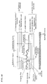
- FIG. 1 is a plan view for showing a configuration of a transflective type LCD related to a first embodiment of the present invention
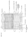
- FIG. 2 is a cross-sectional view in A-A' line of FIG. 1.
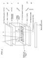
- FIG. 3 is an illustration for showing a polarization state in each position of the transflective type LCD related to the first embodiment of the present invention
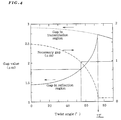
- FIG. 4 is a graph for showing a relationship between a twist angle and a gap.
- FIG. 5 are graphs for showing V-T characteristics under predetermined condition. Note here that the present embodiment features that an irregular film is formed also in the transmission region as in the reflection region in order to provide the same gap in these regions.
- the transflective type LCD of the present embodiment comprises the active matrix substrate 12, the opposing substrate 16, the liquid crystal layer 17 sandwiched by these substrates, the back-light source 18 arranged below the active matrix substrate 12, and the phase difference plates 20a and 20b as well as the polarizing plates 19a and 19b respectively arranged on the outer sides of the active matrix substrate 12 and the opposing substrate 16.
- the active matrix substrate 12 further comprises the gate line 1, the gate electrode 1a, the common storage line 4, the auxiliary capacitance electrode 4a, the gate insulation film 9, the semiconductor layer, the data line 2, the source/drain electrode, and the capacitance accumulation electrode 2c which are formed on the transparent insulation substrate 8 and, on the passivation film 10 covering these, the same shaped irregular film 11 in both the transmission and reflection regions.
- the transparent electrode film 5 made of ITO etc.
- the reflection electrode film 6 made of metal such as Al/Mo.
- the reflection region and the transmission regions have the irregular film 11 with the same shape formed therein and so have almost the same height (specifically with a difference in height of 1 ⁇ m or less), thus giving almost the same gap of the liquid crystal layer 17 in themselves.
- the phase difference plate ( ⁇ /4 plate) 20b is arranged between the liquid crystal layer 17 and the polarizing plate 19b.
- ⁇ /4 plate 20b By then turning the ⁇ /4 plate 20b by 45 degree with respect to the optical axis of the polarizing plate 19b and sandwiching it therebetween, linear-polarized (horizontal) light passing through the polarizing plate 19b is transformed into clockwise circular-polarized light.
- This clockwise circular-polarized light arrives at the reflection electrode film 6 as linear-polarized light by setting a gap d1 at a predetermined value.
- the linear-polarized light is reflected by the reflection electrode film 6 as linear-polarized light, which in turn goes out of the liquid crystal layer 17 as clockwise circular-polarized light.
- This circular-polarized light is transformed by the ⁇ /4 plate 20b into linear-polarized (horizontal) light and then goes out of the polarizing plate 19b having the horizontal optical axis, thus giving white display.
- the liquid crystal is erected.
- light injected to the liquid crystal layer 17 as circular-polarized clockwise arrives at the reflection electrode film 6 as clockwise circular-polarized light, which in turn is reflected by the reflection electrode film 6 as counterclockwise circular-polarized light.
- display appears black.
- arrangement angles of the optical axes of the ⁇ /4 plate 20a and the polarizing plate 19a on the lower side are determined so that display may appear black with a voltage applied on the liquid crystal.
- the lower side polarizing plate 19a is arranged in a crossed Nicols manner, that is, as turned by 90 degree with respect to the upper side polarizing plate 19b. Further, in order to cancel (compensate for) an influence by the upper side ⁇ /4 plate 20b, the lower side ⁇ /4 plate 20a is also arranged as turned by 90 degree.
- the liquid crystal Since the liquid crystal is erected when a voltage is applied thereon, the light is unchanged in polarization state, so that essentially it is optically equal to a state where the polarizing plates 19a and 19b are arranged in the crossed Nicols manner, thus providing black display with a voltage applied.
- the arrangement of the optical members of the transflective liquid crystal panel and the arrangement angles of their optical axes are determined.
- FIG. 4 shows respective gaps d1 and d2 of the reflection region and the transmission region which are optimal to maximize of reflectivity and transmittivity of a white color when the optical members are arranged at the above-mentioned arrangement angles and the twist angle ⁇ of the liquid crystal is changed over 0-90 degree.
- FIG. 4 indicates that the optimal gap of the transmission region is the same as that of the reflection region at a liquid crystal twist angle of 72° and also that as the liquid crystal twist angle decreases, the optimal gap of the reflection region becomes smaller than that of the transmission region.
- FIG. 5A shows the voltage-luminance characteristics (V-T characteristics) of the panel in the transmission and reflection modes under these conditions.
- FIGS. 5 show that in the configuration of the present embodiment the V-T characteristics of the transmission mode agree well with those of the reflection mode and also the irregular films 11 can be formed in the same shape throughout the surface of the pixel region to provide almost the same gap of the liquid crystal as well as almost the same V-T characteristics both in the reflection and transmission regions, thus improving the display quality.
- the irregular films 11 having the same shape have been formed not only in the reflection region but also in the transmission region, the irregular films 11 may not be the same in shape as far as the reflection and the transmission regions have substantially the same gap.
- the first insulation film may be formed in two steps so as to be a little thicker in the reflection region where it is scattered in dot taking into account a change in shape of thereof, thus providing almost the same total film thickness including the thickness of the second insulation film in these two regions.
- the present embodiment features that to suppress a reaction between the transparent electrode film made of ITO etc. and the reflection electrode film made of Al/Mo etc., the positional relationship these electrode films is regulated.
- the transflective type LCD 12 of the present embodiment comprises the active matrix substrate 12, the opposing substrate 16, and the liquid crystal layer 17 sandwiched by these substrates in such a configuration that on the outer sides of the active matrix substrate 12 and the opposing substrate 16 are respectively arranged the ⁇ /4 plates and the polarizing plates at the above-mentioned arrangement angle with respect to the optical axis.
- the opposing substrate is further comprised of a color filter and an opposing electrode for supplying a reference potential.
- the gate line 1 for supplying a scanning signal
- the common storage line 4 which gives capacitance
- the auxiliary capacitance electrode 4a the data line 2 for supplying an image signal
- the TFT 3 connected as a switching element to an intersection of these, and a pixel electrodes arranged in matrix at each of the transistors.
- To the gate electrode 1a of the TFT 3 is connected the gate line 1 and, to its drain electrode is connected the data line 2.
- the passivation film 10 is formed thereon, on which is in turn formed the irregular layer 11 made of photo-sensitive acrylic resin which underlies the irregularities of the reflection electrode film 6.
- the transparent electrode film 5 composed of a transparent conductive film made of ITO etc., on which is formed the reflection electrode film 6 made of high-reflectivity metal such as Al.
- the transparent electrode film 5 and the reflection electrode film 6 are separated from each other in a region between the adjacent pixels, in which region of the transparent electrode film 5 is eroded at its edge when the reflection electrode film 6 is patterned, thus giving a defective pixel in some cases.
- the present patent application employs a variety of countermeasures.
- One is to adjust the positional relationship between the reflection electrode film 6 and the transparent electrode film 5. Specifically, as shown in FIG. 6, a window portion which provides a transmission region is formed in the reflection electrode film 6 in each of the pixels to thereby set a positional relationship between the reflection electrode film 6 and the transparent electrode film 5 so that these two films may overlap with each other around the overall periphery of this window portion.
- one cause of erosion is considered as follows: at the edge of the transparent electrode film 5 the reflection electrode film 6 deposited thereon has poor coverage due to a crack etc., through which a developer soaks into the poor coverage portion when forming a resist pattern for reflection electrode film 6. To guard against this, a predetermined overlap region is provided between the transparent electrode film 5 and the reflection electrode film 6 to cover the edge of the transparent electrode film 5 with a resist pattern in order to prevent the developer from coming in direct contact therewith, thus avoiding erosion of the transparent electrode film 5. Note here that an extent of the overlapping should be enough only to cover the poor coverage portion, which is specifically 2 ⁇ m or so as confirmed experimentally by the present inventor.
- the reflection electrode film 6 in such a manner that it may overlap with the transparent electrode film 5 around its overall periphery, an area in which these two films 5 and 6 come in contact with each other can be increased advantageously. That is, in a case of the reflection region is formed on the side of the TFT 3, the source electrode of the TFT 3 and the reflection electrode film 6 can be interconnected via a contact hole 7 formed through the irregular layer 11 and the passivation film 10 to connect the transparent electrode film 5 to the reflection electrode film 6 in order to thereby interconnect the source electrode and the transparent electrode film 5, so that contact resistance between the transparent electrode film 5 and the reflection electrode film 6 can be decreased by forming these two films in such a manner that they may overlap with each other around the overall periphery. Moreover, by connecting the transparent electrode film 5 around its overall periphery, such an effect can be expected as to provide a uniform potential everywhere on the transparent electrode film 5, thus accurately controlling a voltage applied on the liquid crystal.
- the present embodiment has been described with reference to a configuration in which one rectangular window portion is formed in the reflection electrode film 6, the present invention is not limited thereto; for example, the window portion may be polygonal, circular, elliptical, or of any other arbitrary shape and be provided more than one in each pixel, as far as the reflection electrode film 6 overlaps with the transparent electrode film 5 around its overall periphery.
- the irregular film 11 is shaped irregular in the reflection region and flat in the transmission region, it may be formed irregular in both of the regions 5 and 6 as shown in FIG. 2 and their surfaces may be of an arbitrary shape.
- FIGS. 8-10 are drawings for explaining problems in production process of the active matrix substrate. Note here that the present embodiment features that the electric erosion reaction is suppressed from occurring between the transparent electrode film and the reflection electrode film.
- FIG. 8B expanded view of a defective portion of FIG. 8A
- a problem that a developer soaks into the reflection electrode film 6 through its crack at the edge of the transparent electrode film 5 during a PR process for processing of the reflection electrode film 6 is solved by adjusting the planar positional relationship between the reflection electrode film 6 and the transparent electrode film 5.
- the present embodiment features a method of adjusting the thickness of the reflection electrode and optimizing a cleaning step before the transparent electrode film 5 is formed to thereby suppress electric erosion from occurring between the reflection electrode film 6 and the transparent electrode film 5.
- the following will describe a mechanism of and how to suppress electric erosion from occurring between the ITO substrate of the transparent electrode film 5 and the Al substrate of the reflection electrode film 6.
- Combination is very bad between an Al-based material, which is highly reactive and easily reacts with oxygen to form an oxide film (Al 2 O 3 ), and ITO, which is an oxide conductor.
- ITO which is an oxide conductor.
- electric erosion occurs to erode (oxidize) Al and dissolve (reduce) ITO, thus giving poor contact between Al and ITO (see FIG. 8B). This electric erosion reaction is considered to occur by the following mechanism.
- the above-mentioned phenomenon of electric erosion occurring between the Al and ITO substances can be suppressed to some extent by inserting Mo etc. as the barrier metal between these substances.
- the Al and Mo substances deposited by sputtering are generally columnar crystal, so that a developer soaks into them through a gap between the columns to touch off electric erosion if Al and Mo do not have sufficient film thickness.
- the present inventor investigated an extent to which the electric erosion reaction occurs when the film thickness of Al and Mo formed on the ITO are changed respectively. A correlation between these is given in a table below. In the table, X indicates significant occurrence of electric erosion, ⁇ indicates partial occurrence, ⁇ indicates almost no occurrence, and o ⁇ indicates no occurrence.
- Mo film thickness Al film thickness Electric erosion 50 nm (500 A) 50 nm ⁇ 100 nm ⁇ 200 nm ⁇ 100 nm 50 nm ⁇ 100 nm ⁇ 200 nm ⁇ 200 nm 50 nm ⁇ 100 nm ⁇ 200 nm ⁇ 100 nm twice 50 nm ⁇ 100 nm ⁇ 200 nm o ⁇ 100 nm twice o ⁇
- Table 1 indicates that to suppress electric erosion from occurring, it is necessary to form both Mo and Al films to a film thickness of 100 nm (1000 ⁇ ) or more, preferably 200 nm or more. Furthermore, it was found that when forming the Mo and Al films, rather than forming them, for example, to a thickness of 200 nm at a time, preferably they are formed to a thickness of 100 nm, then washed with an alkali solution once, and then formed to another thickness of 200 nm, in order to improve their performance as a barrier.
- the reason may be that the surface of Mo dissolves by alkali washing and is reduced in columnar-ness, so that when once exposed to the air or the washing solution, the Mo surface has a thin film formed thereon and, when formed second time, is changed in crystallinity.
- Paragraphs (1) and (2) have described how to improve the performance of barrier metal. No matter how the barrier metal performance is improved, however, unless the transparent electrode film 5 made of ITO is patterned with good adhesiveness on the underlying irregular film 11, the developer soaks through a gap into the reflection electrode film 6 to give rise to electric erosion as shown in FIG. 8C.
- UV ray Prior to sputtering of the ITO, ultra-violet (UV) ray is applied to decomposes an organic substance such as oil and then pure water or a weak alkali solution is used for washing, a step of which washing was experimentally confirmed by the present inventor to have an influence on the adhesiveness of the ITO.
- Table 2 shows a correlation between electric erosion and an application quantity of UV ray prior to ITO sputtering.
- UV ray with a wavelength of 300 nm was applied with a quantity of 0 mJ through 1 J.
- Table 2 indicates that electric reaction is liable to occur at a quantity of 100 mJ or more of UV ray application.
- a mechanism for that is considered as follows: a polymer network on the surface of the irregular film 11 made of an organic substance such as acrylic is destroyed by UV ray and, when an ITO film is formed thereon and patterned by photolithography (PR), the surface of the irregular film 11 on which the polymer network is destroyed dissolves in an etch-off solution during an etch-off step, thus causing the edge of the ITO to lift.
- a lift cannot completely be covered by barrier metal, if provided to the reflection electrode film 6.
- a resist pattern 21 used for processing of the reflection electrode film does not cover the edge of the ITO, so that a developer soaks through a gap between the electrodes during a developing step, thus giving rise to electric erosion as confirmed by the experiment.
- the resist pattern used to etch the reflection electrode film 6 also covers the edge of the ITO to thereby block the developer, thus preventing it from disadvantageously soaking through during the developing step.
- the washing step prior to ITO sputtering by limiting the application quantity of UV ray down to 100 mJ or less or even by eliminating the UV ray application step and also by setting the film thickness of both the barrier metal and Al films of the reflection electrode film 6 at 100 nm or more, preferably 200 nm or more, it is possible to efficiently suppress electric erosion between the ITO and Al substances, thus preventing the conventional dissolving of ITO and Al (see a microscopic picture of FIG. 10).
- the barrier metal is not limited to it but may be Cr, Ti, W, etc. instead.
- the film thickness of the Al and Mo substances have been set at 100 nm or more, preferably 200 nm or more, the optimal film thickness may be adjusted appropriately corresponding to the film formation conditions including sputtering etc.
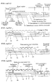
- FIGS. 11 and FIGS. 12 are cross-sectional flow diagrams for showing a transflective type LCD manufacturing method related to a fourth embodiment of the present invention
- FIGS. 13 are the cross-sectional flow diagrams for showing the method for forming the irregularity film.
- the present embodiment gives a specific manufacturing method which enables G-D conversion to prevent short-circuiting of a leader wiring owing to a conductive seal in addition to taking into account the conditions described with the above-mentioned embodiments. The method is described with reference to these figures.
- metal such as Cr is deposited on the transparent insulation substrate 8 made of glass and patterned with publicly known photolithography and etching technologies to form the gate line, the gate electrode 1a, the common storage line, and the auxiliary capacitance electrode 4a.
- a semiconductor layer made of a-Si etc. is deposited via the gate insulation layer film 9 made of SiO 2 , SiNx, SiON, etc. and patterned into islands, on which metal such as Cr is in turn deposited and patterned to form the data line, the drain electrode 2a, the source electrode 2b, and the capacitance accumulation electrode 2c.
- the passivation film 10 made of SiNx etc. for protecting the TFT 3 is formed with plasma-enhanced CVD, after which the gate insulation film 9 and the passivation film 10 at the G-D conversion portion and the terminal portions are partially removed to form a contact hole. Then, a conductive material made of ITO, Al, etc. is deposited to form a terminal electrode 23 and a G-D conversion electrode 22 for interconnecting the drain and gate layers at the G-D conversion portion.
- an irregular film 11 is formed.
- This irregular film 11 is formed by applying photo-sensitive acrylic resin, for example, PC403, 415G, 405G, etc. made by JSR Co. using spin coating. Furthermore, the photo-sensitive acrylic resin is under-exposed with a little smaller quantity of exposure in an expected recess region of the irregularities, not exposed on an expected protrusion region of them, and exposed with a sufficient quantity of exposure in the expected contact hole region.
- a half-tone (gray tone) mask can be used on which a reflection film is formed at a portion which corresponds to the expected protrusion region, a transmission mask is formed at a portion which corresponds to the expected contact hole region, and a transflective film is formed at a portion which corresponds to the expected recess region, thus requiring exposing only once to form the irregularities.
- a half-tone (gray tone) mask can be used on which a reflection film is formed at a portion which corresponds to the expected protrusion region, a transmission mask is formed at a portion which corresponds to the expected contact hole region, and a transflective film is formed at a portion which corresponds to the expected recess region, thus requiring exposing only once to form the irregularities.
- an ordinary mask comprised of only reflection/transmission films can be used to form the irregularities by exposing the expected contact hole and recess regions separately with different exposure quantities.
- an alkali developer is used to form the irregularities by utilizing a difference in dissolving rate in an alkali solution of the expected recess, protrusion, and contact hole regions.
- the acrylic film is decolorized by exposing the overall surface to suppress transmission light from being attenuated by the irregular mask 11. Then, the surface is cured, for example, at 220°C for one hour to form the irregular film 11 having a desired shape.
- this irregular mask 11 may be formed by forming one layer of photo-sensitive acrylic resin and then changing an exposure quantity partially, it may be formed using a plurality of photo-sensitive acrylic resin.
- desired irregularities can be formed by forming first layer of photo-sensitive acrylic resin in a shape of islands, then heat treating it to form the first insulation film 11a, then applying thereon the second insulation film 11b made of photo-sensitive acrylic resin having a predetermined value of viscosity, and then filling the gap between the islands of the first insulation film 11a.
- a transparent conductive film made of ITO etc. is formed by sputtering, in which step preferably a UV application quantity is 100 mJ or less as described with the third embodiment. Then, thus formed ITO is patterned into a predetermined shape to form the transparent electrode film 5 in the transmission region.
- Mo is used as barrier metal to suppress electric erosion between ITO and Al of the reflection electrode, to form Mo and Al films which act as the barrier metal and the reflection metal respectively.
- the Mo and Al films are formed to a thickness of 100 nm or more, preferably 200 nm or more and also in two steps to suppress the columnar crystal from growing by sputtering.
- the Al/Mo films are collectively wet-etched to pattern the reflection electrode film 6.
- the positional relationship of the Al/Mo films is set so that they may overlap with each other around the overall periphery of the ITO.
- this method of manufacturing the active matrix substrate makes it possible to obtain a transflective type LCD in which the peeling of the transparent electrode film 5 and the electric erosion between the transparent electrode film 5 and the reflection electrode film 6 can be suppressed to prevent occurrence of a defective pixel and also G-D conversion is conducted around the outer periphery of the liquid crystal panel.
- FIGS. 14 and 15 are cross-sectional flow diagrams for showing the transflective type LCD manufacturing method related to a fifth embodiment of the present invention.
- the present embodiment has simplified the manufacturing method as compared to the fourth embodiment. The method is described below with reference to these figures.
- the gate line, the gate electrode 1a, the common storage line, and the auxiliary capacitance electrode 4a on which are sequentially formed the gate insulation film 9, the semiconductor layer, the data line, the drain electrode, the source electrode, and the capacitance accumulation electrode 2c.
- the passivation film 10 which protects the TFT 3 is formed, the gate insulation film 9 and the passivation film 10 at the G-D conversion portion and the terminal portion are etched off to form a contact hole.
- the present embodiment simplifies the manufacturing steps by using the transparent electrode film 5 and the reflection electrode film 6 which are formed in the subsequent steps, to interconnect the drain and gate layers of the G-D conversion portion and form the terminal electrode.
- the irregular film 11 is formed to form irregularities of the reflection electrode film 6.
- the photo-sensitive acrylic resin is under-exposed with a little smaller quantity of exposure in an expected recess region of the irregularities, not exposed on an expected protrusion region of them, and exposed with a sufficient quantity of exposure in the expected contact hole 7 region.
- an alkali developer is used to form the irregularities by utilizing a difference in dissolving rate in an alkali solution of these regions.
- the surface is thoroughly exposed to decolorize the acrylic film and cured, for example, at 220°C for one hour to form the irregular film 11.
- a transparent conductive film made of ITO etc. is formed by sputtering and patterned to form the transparent electrode film 5 in the transmission region.
- ITO is formed also at the terminal portion to form the terminal electrode 23.
- a Mo film with a film thickness of 100 nm or more, preferably 200 nm or more, and an Al film with a film thickness of 100 nm or more, preferably 200 nm or more, are formed consecutively.
- the Al/Mo films are wet-etched collectively to pattern the reflection electrode film 6.
- Al/Mo films are formed also at the G-D conversion portion to interconnect its drain and source layers.
- the layers of the G-D conversion portion are interconnected using the reflection electrode film 6 and the terminal electrode 23 is formed using the transparent electrode film 5, so that it is possible to eliminate the step of forming and patterning the ITO film for G-D conversion etc. in contrast to the fourth embodiment.
- the present embodiment deposits the reflection electrode film 6 in the contact hole 7 to connect it with the source electrode and then with the transparent electrode film 5 at the overlapping portion thereof, the contact may not be enough only with the reflection electrode film 6 in some cases because the irregular film 11 in which the contact hole 7 is formed has a large step.
- the following manufacturing method may be employed.
- the irregular film 11 is formed to form irregularities of a reflection plate.
- the photo-sensitive acrylic resin is under-exposed with a little smaller quantity of exposure in an expected recess region of the irregularities, not exposed on an expected protrusion region of them, and exposed with a sufficient quantity of exposure in the expected contact hole region and then, an alkali developer is used to form the irregularities by utilizing a difference in dissolving rate in an alkali solution of these regions. Then, the surface is thoroughly exposed to decolorize the acrylic film and cured, for example, at 220°C for one hour to form the irregular film 11.
- a transparent conductive film made of ITO etc. is formed by sputtering and patterned to form the transparent electrode film 5 in the transmission region and the terminal electrode 23 as well.
- ITO is deposited also in the contact hole 7 to fill with it completely or partially.
- the Mo film and the reflecting Al metal film each having a film thickness of 100 nm or more, preferably 200 nm or more, are formed consecutively.
- the Al/Mo films are wet-etched collectively to pattern the reflection electrode film 6.
- the reflection electrode film 6 is formed also at the G-D conversion portion to interconnect its drain and source layers.
- the transparent electrode film 5 is already deposited in the contact hole 7, so that even if the contact hole 7 has a large aspect ratio, secure contact can be obtained between the source electrode and the reflection electrode film 6.
- the contact hole provided on the source electrode 2c of the TFT3 continues electrically to the reflection electrode film 6 and the transparent electrode film 5 in this order, so that contact can be secured even if the irregular film 11 is thick and the contact hole 7 has a large aspect ratio.
- the transflective type LCD and method for manufacturing the same according to the present invention has the following effects.
- the V-T characteristics of the transmission mode can agree with those of the reflection mode to thereby improve a display quality.
- the irregular film is formed almost in the same shape everywhere on the surface of the pixel region to thereby provide almost the same gap in both the reflection region and the transmission region mode.
- the second effect it is possible to suppress electric erosion from occurring between the transparent electrode film made of ITO etc. and the reflection electrode film made of Al etc. to thereby prevent occurrence of abnormal display.
- the reflection electrode film is formed in configuration all around the edge of the ITO film to cover the edge with a resist for processing the reflection electrode film when the resist is formed, thus preventing the developer from coming in contact therewith.
- the close contact-ness of the ITO film is improved to prevent the etchant or the developer from soaking through.
Landscapes
- Physics & Mathematics (AREA)
- Nonlinear Science (AREA)
- Mathematical Physics (AREA)
- Chemical & Material Sciences (AREA)
- Crystallography & Structural Chemistry (AREA)
- General Physics & Mathematics (AREA)
- Optics & Photonics (AREA)
- Liquid Crystal (AREA)
- Engineering & Computer Science (AREA)
- Food Science & Technology (AREA)
- Devices For Indicating Variable Information By Combining Individual Elements (AREA)
- Optical Elements Other Than Lenses (AREA)
- Polarising Elements (AREA)
- Thin Film Transistor (AREA)
Priority Applications (3)
| Application Number | Priority Date | Filing Date | Title |
|---|---|---|---|
| EP10196566A EP2372438A1 (fr) | 2001-08-06 | 2002-08-05 | Procédé de fabrication d'un dispositif d'affichage transflectif à cristaux liquides et d'un substrat transflectif à matrice active |
| EP11157140A EP2345924A3 (fr) | 2001-08-06 | 2002-08-05 | Dispositif d'affichage transflectif à cristaux liquides et son procédé de fabrication |
| EP11157148A EP2345925A3 (fr) | 2001-08-06 | 2002-08-05 | Dispositif d'affichage transflectif à cristaux liquides et son procédé de fabrication |
Applications Claiming Priority (2)
| Application Number | Priority Date | Filing Date | Title |
|---|---|---|---|
| JP2001237887 | 2001-08-06 | ||
| JP2001237887A JP3895952B2 (ja) | 2001-08-06 | 2001-08-06 | 半透過型液晶表示装置及びその製造方法 |
Publications (2)
| Publication Number | Publication Date |
|---|---|
| EP1284433A2 true EP1284433A2 (fr) | 2003-02-19 |
| EP1284433A3 EP1284433A3 (fr) | 2003-03-19 |
Family
ID=19068896
Family Applications (4)
| Application Number | Title | Priority Date | Filing Date |
|---|---|---|---|
| EP02017478A Withdrawn EP1284433A3 (fr) | 2001-08-06 | 2002-08-05 | Dispositif d'affichage transflectif à cristaux liquides et son procédé de fabrication |
| EP11157148A Withdrawn EP2345925A3 (fr) | 2001-08-06 | 2002-08-05 | Dispositif d'affichage transflectif à cristaux liquides et son procédé de fabrication |
| EP10196566A Withdrawn EP2372438A1 (fr) | 2001-08-06 | 2002-08-05 | Procédé de fabrication d'un dispositif d'affichage transflectif à cristaux liquides et d'un substrat transflectif à matrice active |
| EP11157140A Withdrawn EP2345924A3 (fr) | 2001-08-06 | 2002-08-05 | Dispositif d'affichage transflectif à cristaux liquides et son procédé de fabrication |
Family Applications After (3)
| Application Number | Title | Priority Date | Filing Date |
|---|---|---|---|
| EP11157148A Withdrawn EP2345925A3 (fr) | 2001-08-06 | 2002-08-05 | Dispositif d'affichage transflectif à cristaux liquides et son procédé de fabrication |
| EP10196566A Withdrawn EP2372438A1 (fr) | 2001-08-06 | 2002-08-05 | Procédé de fabrication d'un dispositif d'affichage transflectif à cristaux liquides et d'un substrat transflectif à matrice active |
| EP11157140A Withdrawn EP2345924A3 (fr) | 2001-08-06 | 2002-08-05 | Dispositif d'affichage transflectif à cristaux liquides et son procédé de fabrication |
Country Status (7)
| Country | Link |
|---|---|
| US (3) | US6853421B2 (fr) |
| EP (4) | EP1284433A3 (fr) |
| JP (1) | JP3895952B2 (fr) |
| KR (3) | KR100570404B1 (fr) |
| CN (1) | CN1196962C (fr) |
| NO (1) | NO20023694L (fr) |
| TW (1) | TW561299B (fr) |
Cited By (5)
| Publication number | Priority date | Publication date | Assignee | Title |
|---|---|---|---|---|
| EP1478033A3 (fr) * | 2003-05-16 | 2005-09-14 | Sel Semiconductor Energy Laboratory Co., Ltd. | dispositif d'affichage |
| EP1736818A1 (fr) * | 2005-06-23 | 2006-12-27 | Sanyo Epson Imaging Devices Corporation | Dispositif d'affichage à cristaux liquides semi-transmissif |
| US7714958B2 (en) | 2005-11-15 | 2010-05-11 | Semiconductor Energy Laboratory Co., Ltd. | Display device |
| US7821613B2 (en) | 2005-12-28 | 2010-10-26 | Semiconductor Energy Laboratory Co., Ltd. | Display device and manufacturing method thereof |
| US9773818B2 (en) | 2005-10-14 | 2017-09-26 | Semiconductor Energy Laboratory Co., Ltd. | Display device having transparent conductive film and metal film |
Families Citing this family (106)
| Publication number | Priority date | Publication date | Assignee | Title |
|---|---|---|---|---|
| JP4689900B2 (ja) * | 2001-08-22 | 2011-05-25 | Nec液晶テクノロジー株式会社 | 液晶表示装置 |
| KR100806166B1 (ko) * | 2001-10-08 | 2008-02-22 | 삼성전자주식회사 | 반사율 향상을 위한 액정표시장치 및 그 제조방법 |
| TWI226965B (en) * | 2001-10-30 | 2005-01-21 | Nec Lcd Technologies Ltd | Semi-transmission type liquid crystal display and fabrication method thereof |
| JP3895600B2 (ja) * | 2002-01-04 | 2007-03-22 | シャープ株式会社 | 液晶表示装置用基板及びそれを備えた液晶表示装置 |
| US7064799B2 (en) | 2002-07-10 | 2006-06-20 | Nec Lcd Technologies, Ltd. | Semi-transmissive-type liquid crystal display device and method for manufacturing same |
| US7209107B2 (en) * | 2002-11-06 | 2007-04-24 | Sharp Kabushiki Kaisha | Liquid crystal display device and manufacturing method for the same |
| TWI358053B (en) * | 2002-12-06 | 2012-02-11 | Samsung Electronics Co Ltd | Liquid crystal display device having a thin film t |
| KR100936905B1 (ko) * | 2002-12-13 | 2010-01-15 | 삼성전자주식회사 | 액정표시장치 및 이의 제조 방법 |
| KR100936954B1 (ko) * | 2002-12-31 | 2010-01-14 | 엘지디스플레이 주식회사 | 반사투과형 액정표시장치와 그 제조방법 |
| KR100491258B1 (ko) * | 2002-12-31 | 2005-05-24 | 엘지.필립스 엘시디 주식회사 | 반사투과형 액정표시장치용 어레이기판과 그 제조방법 |
| JP4052123B2 (ja) * | 2003-01-17 | 2008-02-27 | ソニー株式会社 | 液晶パネル |
| JP4181905B2 (ja) * | 2003-03-25 | 2008-11-19 | アルプス電気株式会社 | 液晶表示パネルおよび液晶表示装置 |
| TW594201B (en) * | 2003-03-28 | 2004-06-21 | Toppoly Optoelectronics Corp | Reflective LCD having two driving matrixes |
| KR100519377B1 (ko) | 2003-04-08 | 2005-10-06 | 엘지.필립스 엘시디 주식회사 | 반사투과형 액정표시장치용 어레이기판 및 그 제조방법 |
| KR100713885B1 (ko) * | 2003-04-14 | 2007-05-07 | 비오이 하이디스 테크놀로지 주식회사 | 반투과형 액정표시장치 |
| KR100531410B1 (ko) * | 2003-04-15 | 2005-11-28 | 엘지.필립스 엘시디 주식회사 | 반사투과형 액정표시장치의 어레이 기판 및 그의 제조 방법 |
| KR100524621B1 (ko) * | 2003-05-23 | 2005-10-28 | 엘지.필립스 엘시디 주식회사 | 반사투과형 액정표시장치 및 그 제조방법 |
| JP4260563B2 (ja) * | 2003-07-17 | 2009-04-30 | アルプス電気株式会社 | 半透過反射型液晶表示パネルおよび半透過反射型液晶表示装置ならびに半透過反射型液晶表示パネルの製造方法 |
| TWI224234B (en) * | 2003-08-12 | 2004-11-21 | Quanta Display Inc | Pixel structure and fabricating method thereof |
| US7274418B2 (en) * | 2003-10-21 | 2007-09-25 | Symbol Technologies, Inc. | Method and system for improving the contrast of LCDs using circular polarization |
| KR101066410B1 (ko) * | 2003-11-14 | 2011-09-21 | 삼성전자주식회사 | 어레이 기판, 그 제조방법 및 이를 갖는 액정 표시 장치 |
| KR100659912B1 (ko) * | 2003-12-03 | 2006-12-20 | 엘지.필립스 엘시디 주식회사 | 액정표시장치 및 그 제조방법 |
| JP2005173037A (ja) * | 2003-12-09 | 2005-06-30 | Fujitsu Display Technologies Corp | 液晶表示装置及びその製造方法 |
| JP4485184B2 (ja) * | 2003-12-15 | 2010-06-16 | 株式会社半導体エネルギー研究所 | 発光装置および電子機器 |
| KR100617037B1 (ko) * | 2003-12-29 | 2006-08-30 | 엘지.필립스 엘시디 주식회사 | 반사투과형 액정표시장치 및 이의 제조방법 |
| KR20050070773A (ko) * | 2003-12-30 | 2005-07-07 | 엘지.필립스 엘시디 주식회사 | 반사형 액정표시소자 및 반투과형 액정표시소자 |
| JP4540355B2 (ja) * | 2004-02-02 | 2010-09-08 | 富士通株式会社 | 液晶表示装置及びその製造方法 |
| KR101064185B1 (ko) * | 2004-02-05 | 2011-09-14 | 삼성전자주식회사 | 어레이 기판 및 이의 제조 방법과, 이를 갖는 액정 표시장치 |
| TWI300863B (en) * | 2004-03-19 | 2008-09-11 | Toppoly Optoelectronics Corp | Transmissive liquid crystal display |
| JP4628693B2 (ja) * | 2004-03-31 | 2011-02-09 | 富士通株式会社 | 液晶表示装置用基板及びその製造方法並びにそれを備えた液晶表示装置 |
| KR100623255B1 (ko) | 2004-05-10 | 2006-09-19 | 삼성에스디아이 주식회사 | 유기 전계 발광 표시 장치 및 그의 제조 방법 |
| JP4761425B2 (ja) * | 2004-05-12 | 2011-08-31 | 株式会社 日立ディスプレイズ | 表示装置および表示装置の製造方法 |
| US7177000B2 (en) * | 2004-05-18 | 2007-02-13 | Automotive Systems Laboratory, Inc. | Liquid crystal display cell structure and manufacture process of a liquid crystal display comprising an opening formed through the color filter and partially the buffer layer |
| JP4016977B2 (ja) * | 2004-09-03 | 2007-12-05 | セイコーエプソン株式会社 | 液晶表示装置、電子機器 |
| JP3861895B2 (ja) * | 2004-09-08 | 2006-12-27 | 三菱電機株式会社 | 半透過型液晶表示装置およびその製造方法 |
| US7271865B2 (en) * | 2004-12-02 | 2007-09-18 | Research Foundation Of The University Of Central Florida, Inc. | General film compensated reflective twisted nematic liquid crystal display |
| KR101147261B1 (ko) * | 2004-12-04 | 2012-05-18 | 엘지디스플레이 주식회사 | 반투과형 박막 트랜지스터 기판 및 그 제조 방법 |
| KR20060069080A (ko) | 2004-12-17 | 2006-06-21 | 삼성전자주식회사 | 박막 트랜지스터 표시판 및 이를 포함하는 액정 표시 장치 |
| JP4127267B2 (ja) * | 2005-01-14 | 2008-07-30 | 三菱電機株式会社 | 表示装置 |
| JP4083752B2 (ja) | 2005-01-31 | 2008-04-30 | 三菱電機株式会社 | アクティブマトリクス基板及びその製造方法 |
| CN100485463C (zh) * | 2005-04-18 | 2009-05-06 | 统宝光电股份有限公司 | 主动元件阵列基板及液晶显示面板 |
| TWI339306B (en) * | 2005-05-09 | 2011-03-21 | Au Optronics Corp | Liquid crystal display panel, active device array substrate and fabricating method thereof |
| KR100648223B1 (ko) * | 2005-05-11 | 2006-11-24 | 비오이 하이디스 테크놀로지 주식회사 | 반투과형 프린지 필드 스위칭 모드 액정표시장치 |
| US8013957B2 (en) * | 2005-05-21 | 2011-09-06 | The Hong Kong University Of Science And Technology | Transflective liquid crystal device and method of manufacturing the same |
| JP2006330021A (ja) * | 2005-05-23 | 2006-12-07 | Mitsubishi Electric Corp | 液晶表示装置 |
| KR20060121370A (ko) * | 2005-05-24 | 2006-11-29 | 삼성전자주식회사 | 액정표시장치의 제조방법과 이에 의한 액정표시장치 |
| JP2007004126A (ja) * | 2005-05-25 | 2007-01-11 | Sanyo Epson Imaging Devices Corp | 液晶装置及び電子機器 |
| KR20060122489A (ko) * | 2005-05-27 | 2006-11-30 | 삼성전자주식회사 | 액정 표시 장치 |
| TWI324264B (en) | 2005-06-29 | 2010-05-01 | Au Optronics Corp | Liquid crystal display |
| TWI279918B (en) * | 2005-06-29 | 2007-04-21 | Quanta Display Inc | A method for forming a liquid crystal display |
| KR101287702B1 (ko) * | 2005-06-30 | 2013-07-24 | 엘지디스플레이 주식회사 | 반사투과형 액정 표시 장치 및 그 제조 방법 |
| CN100394286C (zh) * | 2005-07-14 | 2008-06-11 | 友达光电股份有限公司 | 液晶显示装置 |
| CN100417996C (zh) * | 2005-07-14 | 2008-09-10 | 友达光电股份有限公司 | 液晶显示器的制造方法 |
| KR20070019162A (ko) * | 2005-08-11 | 2007-02-15 | 엘지.필립스 엘시디 주식회사 | 액정 표시 장치 및 이의 제조 방법 |
| TWI314658B (en) * | 2005-09-09 | 2009-09-11 | Au Optronics Corp | Pixel structure of transflective tft lcd panel and fabricating method thereof |
| CN100343734C (zh) * | 2005-09-23 | 2007-10-17 | 广辉电子股份有限公司 | 半穿透半反射液晶显示面板的像素结构及其制造方法 |
| JP4663485B2 (ja) | 2005-11-04 | 2011-04-06 | 三菱電機株式会社 | 薄膜トランジスタアレイ及びその製造方法、半透過型液晶表示装置 |
| US20070132923A1 (en) * | 2005-12-09 | 2007-06-14 | Toppoly Optoelectronics Corp. | Systems for displaying images involving transflective thin film transistor liquid crystal displays |
| KR101174164B1 (ko) * | 2005-12-29 | 2012-08-14 | 엘지디스플레이 주식회사 | 반사투과형 액정표시장치 |
| KR101301731B1 (ko) | 2006-01-19 | 2013-08-30 | 삼성디스플레이 주식회사 | 표시장치 및 그 제조방법 |
| US8023073B2 (en) | 2006-01-26 | 2011-09-20 | Samsung Electronics Co., Ltd. | Color filter display panel, thin film transistor array panel, liquid crystal display thereof, and method thereof |
| KR20070082957A (ko) * | 2006-02-20 | 2007-08-23 | 삼성전자주식회사 | 표시 기판, 이의 제조 방법 및 이를 갖는 표시 장치 |
| KR100862298B1 (ko) * | 2006-02-27 | 2008-10-13 | 김창현 | 이중 피펫, 이를 이용한 수핵난자의 탈핵 및 핵이식 방법및 체세포 복제동물의 생산방법 |
| JP4419972B2 (ja) * | 2006-03-14 | 2010-02-24 | エプソンイメージングデバイス株式会社 | 液晶装置及び電子機器 |
| TWI333112B (en) * | 2006-03-16 | 2010-11-11 | Au Optronics Corp | Liquid crystal driving electrode and liquid crystal display using the same |
| CN100410746C (zh) * | 2006-04-06 | 2008-08-13 | 友达光电股份有限公司 | 液晶驱动电极构造 |
| US7589703B2 (en) * | 2006-04-17 | 2009-09-15 | Au Optronics Corporation | Liquid crystal display with sub-pixel structure |
| KR20070109521A (ko) * | 2006-05-11 | 2007-11-15 | 삼성전자주식회사 | 박막트랜지스터 기판, 그를 포함하는 액정 표시 패널, 및그 액정 표시 패널의 제조 방법 |
| KR100744401B1 (ko) * | 2006-06-07 | 2007-07-30 | 비오이 하이디스 테크놀로지 주식회사 | 반투과형 액정표시장치의 어레이 기판 및 이의 제조 방법 |
| TW200807067A (en) * | 2006-07-21 | 2008-02-01 | Wintek Corp | Transflective liquid crystal display |
| US20080049176A1 (en) * | 2006-08-25 | 2008-02-28 | Samsung Electronics Co., Ltd. | Thin film transistor-array substrate, transflective liquid crystal display device with the same, and method for manufacturing the same |
| TW200815859A (en) * | 2006-09-19 | 2008-04-01 | Epson Imaging Devices Corp | Liquid crystal display device |
| CN101589331B (zh) * | 2007-01-24 | 2011-06-22 | 夏普株式会社 | 液晶显示装置 |
| US20100020278A1 (en) * | 2007-03-15 | 2010-01-28 | Tetsuo Fujita | Liquid crystal display device and production method thereof |
| KR101264717B1 (ko) * | 2007-03-26 | 2013-05-16 | 엘지디스플레이 주식회사 | 반투과형 액정표시패널 및 그 제조방법 |
| JP2007193371A (ja) * | 2007-04-26 | 2007-08-02 | Advanced Display Inc | 液晶表示装置 |
| TW200844548A (en) * | 2007-05-01 | 2008-11-16 | Au Optronics Corp | Display |
| KR101420428B1 (ko) * | 2007-10-09 | 2014-07-17 | 엘지디스플레이 주식회사 | 액정표시장치 및 그 제조방법 |
| JP4205144B2 (ja) * | 2007-10-12 | 2009-01-07 | 三菱電機株式会社 | アクティブマトリクス基板及びその製造方法 |
| JP2009111201A (ja) * | 2007-10-31 | 2009-05-21 | Mitsubishi Electric Corp | 積層導電膜、電気光学表示装置及びその製造方法 |
| CN102253546A (zh) * | 2007-11-13 | 2011-11-23 | 友达光电股份有限公司 | 像素结构 |
| KR101522241B1 (ko) * | 2008-12-16 | 2015-05-21 | 엘지디스플레이 주식회사 | 시야각 제어가 가능한 액정표시장치 및 그 제조방법 |
| KR101582941B1 (ko) | 2008-12-24 | 2016-01-08 | 삼성디스플레이 주식회사 | 유기 발광 표시 장치 및 그 제조 방법 |
| JP5262966B2 (ja) * | 2009-04-30 | 2013-08-14 | ソニー株式会社 | 表示装置および表示装置の製造方法 |
| TWI385455B (zh) * | 2009-05-22 | 2013-02-11 | Au Optronics Corp | 半穿透半反射式畫素結構及顯示面板 |
| US8665192B2 (en) * | 2009-07-08 | 2014-03-04 | Hitachi Displays, Ltd. | Liquid crystal display device |
| CN102062967B (zh) * | 2009-11-13 | 2013-03-13 | 上海天马微电子有限公司 | 液晶显示装置 |
| WO2011081041A1 (fr) | 2009-12-28 | 2011-07-07 | Semiconductor Energy Laboratory Co., Ltd. | Dispositif à semi-conducteurs et son procédé de fabrication |
| KR101842865B1 (ko) * | 2009-12-28 | 2018-03-28 | 가부시키가이샤 한도오따이 에네루기 켄큐쇼 | 액정 표시 장치 및 전자 기기 |
| WO2011081010A1 (fr) | 2009-12-28 | 2011-07-07 | Semiconductor Energy Laboratory Co., Ltd. | Dispositif d'affichage à cristaux liquides et dispositif électronique |
| US9000438B2 (en) | 2010-02-26 | 2015-04-07 | Semiconductor Energy Laboratory Co., Ltd. | Semiconductor device and manufacturing method thereof |
| KR101790161B1 (ko) * | 2010-08-09 | 2017-10-26 | 삼성디스플레이 주식회사 | 광 센서, 광 센서의 제조 방법, 및 광 센서를 포함하는 액정 표시 장치 |
| CN102645774B (zh) * | 2011-02-22 | 2016-05-04 | 上海天马微电子有限公司 | 一种液晶显示装置 |
| US8709920B2 (en) * | 2011-02-24 | 2014-04-29 | Semiconductor Energy Laboratory Co., Ltd. | Method for manufacturing semiconductor device |
| KR101128063B1 (ko) | 2011-05-03 | 2012-04-23 | 테세라, 인코포레이티드 | 캡슐화 층의 표면에 와이어 본드를 구비하는 패키지 적층형 어셈블리 |
| US8404520B1 (en) | 2011-10-17 | 2013-03-26 | Invensas Corporation | Package-on-package assembly with wire bond vias |
| KR20130114996A (ko) | 2012-04-10 | 2013-10-21 | 삼성디스플레이 주식회사 | 표시 장치 및 그 제조방법 |
| KR102082794B1 (ko) | 2012-06-29 | 2020-02-28 | 가부시키가이샤 한도오따이 에네루기 켄큐쇼 | 표시 장치의 구동 방법, 및 표시 장치 |
| US9583411B2 (en) | 2014-01-17 | 2017-02-28 | Invensas Corporation | Fine pitch BVA using reconstituted wafer with area array accessible for testing |
| CN104777649A (zh) * | 2015-04-21 | 2015-07-15 | 合肥鑫晟光电科技有限公司 | 显示基板及其制备方法、显示装置 |
| KR102471130B1 (ko) * | 2016-02-17 | 2022-11-29 | 삼성디스플레이 주식회사 | 표시 장치 및 이의 제조 방법 |
| KR102572128B1 (ko) * | 2016-03-14 | 2023-08-30 | 삼성디스플레이 주식회사 | 유기 발광 표시 장치 |
| CN113219748B (zh) * | 2018-06-29 | 2023-05-26 | 上海天马微电子有限公司 | 一种阵列基板、液晶显示面板及显示装置 |
| CN112014989A (zh) * | 2019-05-31 | 2020-12-01 | 北京小米移动软件有限公司 | 显示模组、显示设备、显示设备控制方法及存储介质 |
| JP7393927B2 (ja) * | 2019-11-29 | 2023-12-07 | シャープ株式会社 | 液晶表示パネル |
| TWI893815B (zh) * | 2024-02-26 | 2025-08-11 | 瀚宇彩晶股份有限公司 | 顯示面板 |
Citations (3)
| Publication number | Priority date | Publication date | Assignee | Title |
|---|---|---|---|---|
| EP0973058A1 (fr) | 1998-02-04 | 2000-01-19 | Seiko Epson Corporation | Dispositif a cristaux liquides et dispositif electronique |
| US6195140B1 (en) | 1997-07-28 | 2001-02-27 | Sharp Kabushiki Kaisha | Liquid crystal display in which at least one pixel includes both a transmissive region and a reflective region |
| EP1113308A1 (fr) * | 1999-07-07 | 2001-07-04 | Matsushita Electric Industrial Co., Ltd. | Dispositif d'affichage a cristaux liquides translucide |
Family Cites Families (30)
| Publication number | Priority date | Publication date | Assignee | Title |
|---|---|---|---|---|
| JPH06188265A (ja) | 1992-12-22 | 1994-07-08 | Matsushita Electric Ind Co Ltd | 半導体装置およびその製造方法 |
| EP0811892A4 (fr) | 1995-12-25 | 1999-11-17 | Nippon Petrochemicals Co Ltd | Structure en lamine pour operation de chauffage |
| JP2955277B2 (ja) | 1997-07-28 | 1999-10-04 | シャープ株式会社 | 液晶表示装置 |
| US6330047B1 (en) * | 1997-07-28 | 2001-12-11 | Sharp Kabushiki Kaisha | Liquid crystal display device and method for fabricating the same |
| CN1246931A (zh) | 1997-12-04 | 2000-03-08 | 平板展示(Fpd)有限公司 | 显示装置 |
| JP3361278B2 (ja) * | 1997-12-26 | 2003-01-07 | シャープ株式会社 | 反射型液晶表示装置とその製造方法、ならびに回路基板の製造方法 |
| JP3410656B2 (ja) | 1998-03-31 | 2003-05-26 | シャープ株式会社 | 液晶表示装置及びその製造方法 |
| KR100394023B1 (ko) * | 1998-08-06 | 2003-10-17 | 엘지.필립스 엘시디 주식회사 | 반투과 반사형 액정표시장치 |
| JP2000075305A (ja) | 1998-09-02 | 2000-03-14 | Toppan Printing Co Ltd | 液晶表示装置用カラーフィルタ及びその製造方法 |
| US7106400B1 (en) * | 1998-09-28 | 2006-09-12 | Sharp Kabushiki Kaisha | Method of making LCD with asperities in insulation layer under reflective electrode |
| JP2000148042A (ja) | 1998-11-12 | 2000-05-26 | Sharp Corp | 電極配線基板の製造方法及び液晶表示装置の製造方法 |
| JP3992393B2 (ja) | 1999-02-25 | 2007-10-17 | 株式会社アドバンスト・ディスプレイ | 反射型液晶表示装置の製造方法及び反射型液晶表示装置の製造用マスク |
| JP3566874B2 (ja) | 1999-03-08 | 2004-09-15 | シャープ株式会社 | 液晶表示装置の製造方法 |
| KR20010004911A (ko) * | 1999-06-30 | 2001-01-15 | 김영환 | 반사형 액정표시장치의 반사판 형성방법 |
| JP3767255B2 (ja) | 1999-07-16 | 2006-04-19 | セイコーエプソン株式会社 | 液晶装置及び電子機器 |
| KR20010015373A (ko) * | 1999-07-20 | 2001-02-26 | 구본준 | 반사투과 액정 표시장치 |
| JP3765203B2 (ja) | 1999-07-29 | 2006-04-12 | 株式会社日立製作所 | 液晶表示装置 |
| JP3498020B2 (ja) * | 1999-09-29 | 2004-02-16 | Nec液晶テクノロジー株式会社 | アクティブマトリックス基板及びその製造方法 |
| JP2001188112A (ja) | 1999-10-21 | 2001-07-10 | Matsushita Electric Ind Co Ltd | 反射板、その製造方法、表示素子、表示装置 |
| JP2001132744A (ja) | 1999-11-05 | 2001-05-18 | Akashi Corp | シャフトの支持方法及び支持機構 |
| KR100655278B1 (ko) * | 1999-12-06 | 2006-12-08 | 삼성전자주식회사 | 반투과 반사형 박막트랜지스터 액정표시장치 |
| KR100656696B1 (ko) | 1999-12-21 | 2006-12-15 | 엘지.필립스 엘시디 주식회사 | 반사투과형 액정 표시장치 |
| JP2001194662A (ja) * | 2000-01-14 | 2001-07-19 | Nec Corp | 反射型液晶表示装置及びその製造方法 |
| TW483038B (en) | 2000-05-26 | 2002-04-11 | Koninkl Philips Electronics Nv | Display device |
| KR100372579B1 (ko) * | 2000-06-21 | 2003-02-17 | 엘지.필립스 엘시디 주식회사 | 액정표시장치용 어레이기판과 그 제조방법 |
| TWI240811B (en) * | 2000-09-13 | 2005-10-01 | Au Optronics Corp | Manufacturing method of liquid crystal display device |
| KR20020057228A (ko) * | 2000-12-30 | 2002-07-11 | 주식회사 현대 디스플레이 테크놀로지 | 하프톤 패터닝을 이용한 반사형 엘시디의 반사판 제조방법 |
| JP5131505B2 (ja) | 2001-04-27 | 2013-01-30 | Nltテクノロジー株式会社 | 液晶表示装置 |
| KR100803109B1 (ko) * | 2001-06-14 | 2008-02-13 | 삼성전자주식회사 | 반사 투과형 액정표시장치 및 이의 제조방법 |
| KR100803165B1 (ko) * | 2001-07-20 | 2008-02-14 | 삼성전자주식회사 | 반사-투과형 액정표시장치 및 그 제조방법 |
-
2001
- 2001-08-06 JP JP2001237887A patent/JP3895952B2/ja not_active Expired - Lifetime
-
2002
- 2002-07-26 US US10/205,365 patent/US6853421B2/en not_active Expired - Lifetime
- 2002-07-29 TW TW091116945A patent/TW561299B/zh not_active IP Right Cessation
- 2002-08-05 EP EP02017478A patent/EP1284433A3/fr not_active Withdrawn
- 2002-08-05 EP EP11157148A patent/EP2345925A3/fr not_active Withdrawn
- 2002-08-05 EP EP10196566A patent/EP2372438A1/fr not_active Withdrawn
- 2002-08-05 NO NO20023694A patent/NO20023694L/no not_active Application Discontinuation
- 2002-08-05 EP EP11157140A patent/EP2345924A3/fr not_active Withdrawn
- 2002-08-06 KR KR1020020046316A patent/KR100570404B1/ko not_active Expired - Fee Related
- 2002-08-06 CN CNB021276617A patent/CN1196962C/zh not_active Expired - Lifetime
-
2004
- 2004-12-13 US US11/009,029 patent/US7817229B2/en not_active Expired - Fee Related
-
2005
- 2005-04-21 KR KR1020050033002A patent/KR100746779B1/ko not_active Expired - Fee Related
- 2005-10-12 KR KR1020050096019A patent/KR100746778B1/ko not_active Expired - Fee Related
-
2010
- 2010-10-15 US US12/905,793 patent/US7990501B2/en not_active Expired - Fee Related
Patent Citations (3)
| Publication number | Priority date | Publication date | Assignee | Title |
|---|---|---|---|---|
| US6195140B1 (en) | 1997-07-28 | 2001-02-27 | Sharp Kabushiki Kaisha | Liquid crystal display in which at least one pixel includes both a transmissive region and a reflective region |
| EP0973058A1 (fr) | 1998-02-04 | 2000-01-19 | Seiko Epson Corporation | Dispositif a cristaux liquides et dispositif electronique |
| EP1113308A1 (fr) * | 1999-07-07 | 2001-07-04 | Matsushita Electric Industrial Co., Ltd. | Dispositif d'affichage a cristaux liquides translucide |
Cited By (16)
| Publication number | Priority date | Publication date | Assignee | Title |
|---|---|---|---|---|
| US7495382B2 (en) | 2003-05-16 | 2009-02-24 | Semiconductor Energy Laboratory Co., Ltd. | Display device having display surfaces with polarizing plates |
| EP1478033A3 (fr) * | 2003-05-16 | 2005-09-14 | Sel Semiconductor Energy Laboratory Co., Ltd. | dispositif d'affichage |
| US7719638B2 (en) | 2005-06-23 | 2010-05-18 | Epson Imaging Devices Corp. | Semi-transmissive liquid crystal display device with signal lines that are broader in the transmissive portion than in the reflective portion |
| EP1736818A1 (fr) * | 2005-06-23 | 2006-12-27 | Sanyo Epson Imaging Devices Corporation | Dispositif d'affichage à cristaux liquides semi-transmissif |
| US9773818B2 (en) | 2005-10-14 | 2017-09-26 | Semiconductor Energy Laboratory Co., Ltd. | Display device having transparent conductive film and metal film |
| US10847547B2 (en) | 2005-10-14 | 2020-11-24 | Semiconductor Energy Laboratory Co., Ltd. | Display device having transparent conductive film and metal film |
| US11296124B2 (en) | 2005-10-14 | 2022-04-05 | Semiconductor Energy Laboratory Co., Ltd. | Display device and manufacturing method thereof |
| US11901370B2 (en) | 2005-10-14 | 2024-02-13 | Semiconductor Energy Laboratory Co., Ltd. | Display device |
| US7714958B2 (en) | 2005-11-15 | 2010-05-11 | Semiconductor Energy Laboratory Co., Ltd. | Display device |
| US7821613B2 (en) | 2005-12-28 | 2010-10-26 | Semiconductor Energy Laboratory Co., Ltd. | Display device and manufacturing method thereof |
| US8634044B2 (en) | 2005-12-28 | 2014-01-21 | Semiconductor Energy Laboratory Co., Ltd. | Display device and manufacturing method thereof |
| US9703140B2 (en) | 2005-12-28 | 2017-07-11 | Semiconductor Energy Laboratory Co., Ltd. | Display device and manufacturing method thereof |
| US10444564B1 (en) | 2005-12-28 | 2019-10-15 | Semiconductor Energy Laboratory Co., Ltd. | Display device and manufacturing method thereof |
| US10739637B2 (en) | 2005-12-28 | 2020-08-11 | Semiconductor Energy Laboratory Co., Ltd. | Display device and manufacturing method thereof |
| US11269214B2 (en) | 2005-12-28 | 2022-03-08 | Semiconductor Energy Laboratory Co., Ltd. | Display device and manufacturing method thereof |
| US12189232B2 (en) | 2005-12-28 | 2025-01-07 | Semiconductor Energy Laboratory Co., Ltd. | Display device and manufacturing method thereof |
Also Published As
| Publication number | Publication date |
|---|---|
| KR100746779B1 (ko) | 2007-08-06 |
| US20030030768A1 (en) | 2003-02-13 |
| EP2345924A2 (fr) | 2011-07-20 |
| JP3895952B2 (ja) | 2007-03-22 |
| CN1402064A (zh) | 2003-03-12 |
| EP2345925A2 (fr) | 2011-07-20 |
| NO20023694L (no) | 2003-02-07 |
| EP1284433A3 (fr) | 2003-03-19 |
| EP2372438A1 (fr) | 2011-10-05 |
| US20110027460A1 (en) | 2011-02-03 |
| EP2345924A3 (fr) | 2011-08-31 |
| KR100746778B1 (ko) | 2007-08-06 |
| US7817229B2 (en) | 2010-10-19 |
| TW561299B (en) | 2003-11-11 |
| KR20050048561A (ko) | 2005-05-24 |
| US7990501B2 (en) | 2011-08-02 |
| CN1196962C (zh) | 2005-04-13 |
| KR20030014132A (ko) | 2003-02-15 |
| KR100570404B1 (ko) | 2006-04-11 |
| US6853421B2 (en) | 2005-02-08 |
| NO20023694D0 (no) | 2002-08-05 |
| KR20050104322A (ko) | 2005-11-02 |
| US20050094067A1 (en) | 2005-05-05 |
| EP2345925A3 (fr) | 2012-02-22 |
| JP2003050389A (ja) | 2003-02-21 |
Similar Documents
| Publication | Publication Date | Title |
|---|---|---|
| US6853421B2 (en) | Transflective type LCD and method for manufacturing the same | |
| JP3908552B2 (ja) | 液晶表示装置及びその製造方法 | |
| EP0617310B1 (fr) | Dispositif d'affichage à cristal liquide du type réflectif et procédé pour sa fabrication | |
| US7525626B2 (en) | Liquid crystal display and method for manufacturing the same | |
| US6184960B1 (en) | Method of making a reflective type LCD including providing a protective metal film over a connecting electrode during at least one portion of the manufacturing process | |
| JP3488681B2 (ja) | 液晶表示装置 | |
| JP2000019563A (ja) | 液晶表示装置 | |
| US8031304B2 (en) | Liquid crystal display device | |
| JP4646018B2 (ja) | 液晶表示装置およびその製造方法 | |
| US6587173B2 (en) | Multidomain liquid crystal display device | |
| JP3513409B2 (ja) | 液晶表示装置およびその製造方法 | |
| US20070188682A1 (en) | Method for manufacturing a display device | |
| KR20020012794A (ko) | 투과반사형 액정 표시장치와 그 제조방법 | |
| KR100268010B1 (ko) | 반사형액정표시소자의반사판및그제조방법 | |
| JP4019080B2 (ja) | 液晶表示装置の製造方法 | |
| JP2000162637A (ja) | 液晶表示装置の製造方法 | |
| KR100692689B1 (ko) | 반투과형 액정표시장치 | |
| KR100682745B1 (ko) | 반투과 액정표시장치 | |
| KR100909415B1 (ko) | 반투과형 액정표시장치 및 이의 제조 방법 | |
| KR20070002391A (ko) | 반투과형 액정표시장치용 어레이 기판 및 그 제조방법 | |
| JP3655917B2 (ja) | 液晶表示装置 | |
| KR20030057072A (ko) | 횡전계방식 액정표시소자 및 그 제조방법 | |
| JP2004004992A (ja) | 配線板および液晶表示装置 |
Legal Events
| Date | Code | Title | Description |
|---|---|---|---|
| PUAI | Public reference made under article 153(3) epc to a published international application that has entered the european phase |
Free format text: ORIGINAL CODE: 0009012 |
|
| PUAL | Search report despatched |
Free format text: ORIGINAL CODE: 0009013 |
|
| AK | Designated contracting states |
Designated state(s): AT BE BG CH CY CZ DE DK EE ES FI FR GB GR IE IT LI LU MC NL PT SE SK TR |
|
| AX | Request for extension of the european patent |
Extension state: AL LT LV MK RO SI |
|
| AK | Designated contracting states |
Kind code of ref document: A3 Designated state(s): AT BE BG CH CY CZ DE DK EE ES FI FR GB GR IE IT LI LU MC NL PT SE SK TR |
|
| AX | Request for extension of the european patent |
Extension state: AL LT LV MK RO SI |
|
| 17P | Request for examination filed |
Effective date: 20030207 |
|
| AKX | Designation fees paid |
Designated state(s): DE FI FR GB NL |
|
| 17Q | First examination report despatched |
Effective date: 20090227 |
|
| RAP1 | Party data changed (applicant data changed or rights of an application transferred) |
Owner name: NEC LCD TECHNOLOGIES, LTD. |
|
| RAP1 | Party data changed (applicant data changed or rights of an application transferred) |
Owner name: NLT TECHNOLOGIES, LTD. |
|
| STAA | Information on the status of an ep patent application or granted ep patent |
Free format text: STATUS: THE APPLICATION IS DEEMED TO BE WITHDRAWN |
|
| 18D | Application deemed to be withdrawn |
Effective date: 20161123 |