EP1284499B1 - Halbleiterwafer für das Testen eines integrierten Schaltkreises während der Herstellung und entsprechendes Herstellungsverfahren - Google Patents
Halbleiterwafer für das Testen eines integrierten Schaltkreises während der Herstellung und entsprechendes Herstellungsverfahren Download PDFInfo
- Publication number
- EP1284499B1 EP1284499B1 EP02255732A EP02255732A EP1284499B1 EP 1284499 B1 EP1284499 B1 EP 1284499B1 EP 02255732 A EP02255732 A EP 02255732A EP 02255732 A EP02255732 A EP 02255732A EP 1284499 B1 EP1284499 B1 EP 1284499B1
- Authority
- EP
- European Patent Office
- Prior art keywords
- pcm
- testline
- array
- sram
- embedded
- Prior art date
- Legal status (The legal status is an assumption and is not a legal conclusion. Google has not performed a legal analysis and makes no representation as to the accuracy of the status listed.)
- Expired - Lifetime
Links
Images


Classifications
-
- H—ELECTRICITY
- H10—SEMICONDUCTOR DEVICES; ELECTRIC SOLID-STATE DEVICES NOT OTHERWISE PROVIDED FOR
- H10B—ELECTRONIC MEMORY DEVICES
- H10B10/00—Static random access memory [SRAM] devices
-
- H—ELECTRICITY
- H10—SEMICONDUCTOR DEVICES; ELECTRIC SOLID-STATE DEVICES NOT OTHERWISE PROVIDED FOR
- H10P—GENERIC PROCESSES OR APPARATUS FOR THE MANUFACTURE OR TREATMENT OF DEVICES COVERED BY CLASS H10
- H10P74/00—Testing or measuring during manufacture or treatment of wafers, substrates or devices
- H10P74/27—Structural arrangements therefor
- H10P74/277—Circuits for electrically characterising or monitoring manufacturing processes, e.g. circuits in tested chips or circuits in testing wafers
-
- H—ELECTRICITY
- H10—SEMICONDUCTOR DEVICES; ELECTRIC SOLID-STATE DEVICES NOT OTHERWISE PROVIDED FOR
- H10B—ELECTRONIC MEMORY DEVICES
- H10B10/00—Static random access memory [SRAM] devices
- H10B10/12—Static random access memory [SRAM] devices comprising a MOSFET load element
Definitions
- the present invention relates to semiconductor devices and, in particular, to in-process electrical testing of integrated circuit (IC) components and process control monitors (PCMs).
- IC integrated circuit
- PCMs process control monitors
- ICs Semiconductor integrated circuits
- substrates such as silicon wafers
- the fabricated components are then interconnected through deposited metal layers, or the like, to form logic or other functions.
- the various ICs formed on the wafer are typically arranged in a grid pattern and are thus separated by vertical and horizontal scribe areas, also called "streets.”
- streets vertical and horizontal scribe areas, also called "streets.”
- the wafer is cut up (diced) into the individual chips (die).
- Each die is mounted in a package and the terminals of the die are connected to the package terminals through a wire bonding operation. It is desirable to verify that such integrated basic components are fabricated according to a design specification and have certain properties or values, e.g., a specified gain, resistance, capacitance, etc. An individual component cannot readily be tested, however, once integrated into a circuit,
- stand-alone copies of such basic components are tested.
- the stand-alone copies are fabricated in some location of the surface of the wafer not occupied by the ICs formed on the wafer, e.g., the scribe areas of the wafer.
- Such stand-alone copies or target components have properties or values of gain, resistance, and the like that are representative of such properties of their IC counterparts since they are fabricated using the same process.
- it may be assumed that the parameters measured for the target components are similar to those of the non-tested integrated components, and it is therefore appropriate to apply the test results for the target components to the integrated components.
- Such a quality control methodology is referred to as "in-process electrical testing.”
- a signal source and measurement device are electrically connected to the stand-alone target component to be tested, or DUT (device under test). Electrical connection is typically effected via microprobes between the DUT and the measurement device.
- DUT device under test
- Various measurement device systems are commercially available.
- the target component is electrically connected to pads.
- Microprobes are used to contact the pads, thereby electrically connecting the signal source and the measurement device to the target component.
- the measurement device is typically used to measure various response or performance parameters of the target component, i.e., parameters that characterize the response or performance of the target component.
- PCM process control monitor
- device monitor device monitor
- PCMs are commonly used to monitor the quality of wafer processing in IC manufacturing. See U.S. Patent Numbers 5,523,252 and 6,194,739B1 for descriptions of PCMs and their associated pads.
- PCMs are incorporated typically in the scribe area between two adjacent dice on a wafer.
- Modern CMOS (complementary metal oxide semiconductor) IC chips incorporate a significant amount of on-chip SRAMs (static random access memories).
- SRAMs static random access memories.
- the embedded SRAMs typically use smaller design rules than the logic CMOS process used to create the circuits in which the SRAMs are embedded.
- PCM testline used to monitor the logic CMOS process is not ideally suited for logic-embedded SRAM ICs. What is needed is a PCM testline designed exclusively for logic-embedded SRAMs.
- US-A-5 903 489 addresses a semiconductor memory device capable to suppress the increase of the chip area of the product chip caused by dust of conductive materials generated when a chemical-mechanical polishing (CMP) technique is employed for planarization of the semiconductor devices arranged on a wafer.
- CMP chemical-mechanical polishing
- the teaching of D1 provides a semiconductor memory device comprising a memory cell area including a plurality of memory cells, a peripheral area including a peripheral circuit for controlling the memory cells, the peripheral area including a scribe area at an outer periphery thereof.
- a first monitoring pattern is disposed in the scribe area, having a level substantially equal to a level of the peripheral circuit, and a second monitoring pattern disposed in an area other than the scribe area, the second monitoring pattern having a level substantially equal to a level of the memory cells. Since the second monitoring pattern having a structure similar to that of the memory cell is disposed in an area other than the scribe area, the CMP process or polyimide removing process for the scribe area does not generate dust of conductive materials from the first monitoring pattern which has a level substantially equal to the level of the peripheral area.
- US-A-5 872 018 describes a method for designing testlines suitable for DRAM chips and other integrated circuits (ICs) and teaches the use of product specific test structures for process monitoring of sub-micron DRAM integrated circuits.
- US-B1-6 194 739 also aims to reduce the amount of wafer surface sacrificed in conjunction with the use of testers, such as pads and target components forming a process monitor or device monitor, and to improve the accuracy of such measurements for a given size tester.
- a wafer configured for in-process testing of electrical components has a plurality of dies disposed on the wafer, wherein adjacent dies are separated from one another by streets.
- An in-line device monitor having a first port, a second port, and a device-under-test substantially in line with one another is placed within a street, where the device-under-test is between the first and second ports and electrically coupled to the first and second ports.
- US-A-5 485 095 is addressed to a need for a more sensitive test circuit and test method for signaling possible out-of-spec resistance shifts, or other type of defect, in a current carrying structure of an integrated circuit.
- US-A-5 485 095 proposes a fabrication test circuit for signaling possible out-of-spec resistance in a current carrying structure of an associated integrated circuit.
- the fabrication test circuit includes a plurality of monitor structures electrically connected in parallel. Each monitor structure has an associated test structure and threshold sensitive device. Each test structure is predesigned relative to the current carrying structure of the integrated circuit such that an out-of-spec resistance in the test structure signals a possible out-of-spec resistance in the current carrying structure.
- the threshold sensitive device of each monitor structure outputs a fail signal when a resistance proportional signal from the associated test structure exceeds a predefined level, the fail signal being representative of out-of-spec resistance in the associated test structure and possible out-of-spec resistance in the current carrying structure of the integrated circuit.
- Monitor means are provided for monitoring the plurality of monitor structures for a fail signal output from at least one monitor structure.
- a semiconductor wafer is configured for in-process testing of integrated circuitry fabricated thereon. At least two die are separated by a scribe area, and each of the die has at least one complementary metal oxide silicon (CMOS) static random access memory (SRAM) array embedded therein among mixed-signal CMOS circuitry.
- CMOS complementary metal oxide silicon
- SRAM static random access memory
- the mixed-signal CMOS circuitry includes devices with larger feature sizes compared to similar devices of the embedded SRAM array.
- a first process control monitor (PCM) testline is included, which has a first layout corresponding to the mixed-signal CMOS circuitry.
- a second PCM testline is included, which has a second layout corresponding to the embedded SRAM arrays. The first and second PCM testlines are formed in the scribe area.
- the second PCM testline comprises at least one 6-transistor memory cell.
- the second PCM testline comprises at least one decoder, and/or at least one sense amplifier, and/or at least one data output circuit.
- the second PCM testline comprises facsimiles of embedded SRAM array devices located at different locations within the embedded SRAM array, thereby permitting in-process testing to evaluate process variations that are location specific.
- the second PCM testline comprises facsimiles of embedded SRAM array devices located at different locations within the embedded SRAM array, thereby permitting in-process testing to track across-die variations of critical dimensions.
- the second PCM testline comprises facsimiles of embedded SRAM array devices located at different locations within the embedded SRAM array, thereby permitting in-process testing to track across-die alignment variations.
- the second PCM testline comprises facsimiles of embedded SRAM array devices located at different locations within the embedded SRAM array, thereby permitting in-process testing to track across-wafer variations of critical dimensions.
- the second PCM testline comprises facsimiles of embedded SRAM array devices located at different locations within the embedded SRAM array, thereby permitting in-process testing to track across-wafer alignment variations,
- FIG. 1 shows a conventional prior art wafer having a plurality of dies arranged thereon
- FIG. 2 is an enlarged view of a region of the wafer of FIG. 1 , showing horizontal and vertical streets located between dies;
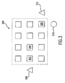
- FIG. 3 shows an array of like devices that may experience different optical effects during photolithograph
- FIG. 4 shows SRAM PCMs, in accordance with an embodiment of the present invention.
- chip integrated circuit
- monolithic device semiconductor device and microelectronic device
- present invention is applicable to all of the above as they are generally understood in the field.
- pins, pads and leads refer to input and/or output terminals of a connector, device, chip, printed circuit, or the like, which are used to provide electrical connection to one or more connectors, devices, chips, printed circuits, or the like.
- metal line trace, wire, conductor, signal path and signalling medium are all related. These related terms are generally interchangeable and appear in order from most specific to most general. In this field, metal lines are sometimes referred to as traces, wires, lines, interconnect or simply metal.
- Metal lines generally aluminum (Al) or an alloy of Al and copper (Cu), are conductors which provide signal paths for coupling, or interconnecting, electrical circuitry. Conductors other than metal are available in microelectronic devices.
- Materials such as doped polysilicon, doped single-crystal silicon (often referred to simply as diffusion, regardless of whether such doping is achieved by thermal diffusion or ion implantation), titanium (Ti), molybdenum (Mo), or refractory metal silicides are examples of other conductors.
- Signalling medium is the most general term and encompasses the others.
- FIG. 1 there is shown a conventional wafer 100 and a plurality of dies 102 formed thereon.
- the dies 102 are discrete regions of the wafer at which circuitry (the IC) is patterned. All dies resident on a wafer may contain the same circuitry, such as is typical for mass production of a particular IC, or each die in a plurality of such dies disposed on a single wafer may have a different circuit configuration from other dies on the wafer.
- the wafer is diced to separate the dies 102 for use. When separated, the individual dies are typically referred to as an IC or chip.
- FIG. 2 there is shown an enlarged view of region 200 of wafer 100 of FIG. 1 .
- Adjacent dies such as adjacent dies 102a and 102b, and adjacent dies 102a and 102c, are separated by respective vertical and horizontal scribe areas (also called streets) 202a, 202b.
- PCMs or testers 204 operable to test various stand-alone electrical components, counterparts of which stand-alone components are incorporated within the circuits comprising any of the dies 102 on wafer 100, are located in the scribe areas between such dies, such as the scribe areas 202a, 202b.
- an edge device 302 is not surrounded on all four sides by similar devices, but may be adjacent to a different device 304 on one side, and a like device 306 on the other side.
- a comer device 308 may be adjacent to one or more different device types 310 and 312.
- edge and corner devices can be exposed to optical effects during photolithography that devices in the center of an array of common devices do not experience during processing. Such process variations can impact operational characteristics of the variously positioned devices (i.e., how the circuits behave).
- CMOS SRAM memory arrays are often laid-out (or "embedded") at various, non-symmetric locations of the circuit.
- edge and comer memory cells of each embedded SRAM memory array are often located adjacent different devices or components.
- the inventors have observed that embedding of SRAM memory arrays can cause operating characteristics of the center, edge, and corner memory cells to vary. Additionally, the inventors have observed that memory array edge and corner cells fail more often than middle cells. This variation of operating characteristics between cells located at different regions of an array and increased failure rates of edge and comer cells may be attributable to optical effects during photolithography. Based on these observations, the inventors have developed a new in-process electrical testing technique to measure and compensate for such variations,
- the SRAM memory arrays are embedded, they are not provided with separate pinouts. Thus, direct in-process testing is of the embedded SRAM memory arrays is not possible Adding pinouts for testing embedded SRAM memory arrays is not practical.
- FIG. 4 illustrates the scribe areas -202a and 202b discussed above.
- a exemplary die 402 comprises standard CMOS logic 404 in which SRAM memory arrays 406 are embedded.
- the standard (e.g., mixed-signal) CMOS logic circuitry 404 comprises devices with larger feature sizes compared to similar devices of the embedded SRAM memory arrays 406.
- SRAM PCM testlines 408 comprise transistors that are laid-out in a manner that is identical to the layout of the on-chip SRAM memory arrays 406. However, independent access is provided to the terminals of the individual transistors (not shown).
- PCMs 410 corresponding to the standard CMOS logic 404 are also formed as part of the testlines.
- the PCMs 408 and 410 can be arranged in the scribe areas in many different patterns. For example, PCMs 408 can be formed in the vertical scribe areas and PCMs 410 can be formed in the horizontal scribe areas, or vice versa. PCMs 408 and 410 can be formed in alternating patterns in both the vertical horizontal scribe areas. Alternatively, PCMs 408 and 410 can be formed in any application specific manner in accordance with the teaching herein, as would be apparent to a person skilled in the relevant art.
- SRAM testline 408 includes transistors from memory , a memory cell, an edge and a corner of the memory array to monitor process variations. Based on such testing using the techniques of the present invention, layout modifications, process modifications, or combinations thereof can be made on subsequent design and tape-out iterations to compensate for such process variations.
- testline of the present invetion is designed to include variations to dimensions of the (a) active region - the channel of the transistor, (b) gate length of the transistor, and (c) size of the contacts.
- the magnitude of the variations is determined by the extent of across-die uniformity that the process technology can provide, as would be apparent to a person skilled in the relevant art.
- the SRAM PCM testlines 408 include a speed path having address loading, address decoding, data sensing, and data output circuits, and the like to facilitate monitoring of the speed path in the embedded SRAM. More specfically, to monitor the junction leakage of P+ to Nwell, or N+ to Psubstrate, a test memory array is generated with all P+ nodes connected in parallel using metal interconnect to a terminal, and similarly all N+ nodes to another terminal. Such a test device can be used to monitor the extent of junction leakage in a SRAM array in production. Also, across-wafer variation of all transistor and junction parameters can be monitored.
- testline testline to monitor the cycle time of a memory, which is the speed at which data can be accessed from the memory, a full access path is placed in the SRAM testline. This consists of loading of the address on the latches, subsequent decoding and data access and data output. The data access path can be monitored as a delay chain or as a ring oscillator. Such a test circuit provides a vehicle to monitor the memory performance. Other test circuits will become apparent to those persons skilled in the art in view of the teachings of the present invention.
- testline can include a sensitive sense amplifier so that the actual sensing circuit of the SRAM 406 can be monitored for manufacturing variations.
- Prior art typically uses a standard CMOS logic testline to monitor process quality. Such testlines do not provide accurate information about how process variations affect SRAM performance. In addition, with prior art critical dimension and overlay variations are not included.
- the advantages of the proposed testline is that it enables regular accurate monitoring of across-die variation of device parameters associated with a SRAM array and thus reduce yield improvement cycle.
Landscapes
- Testing Or Measuring Of Semiconductors Or The Like (AREA)
- For Increasing The Reliability Of Semiconductor Memories (AREA)
Claims (10)
- Halbleiter-Wafer (100), der zur Fertigungsprüfung darauf hergestellter integrierter Schaltung konfiguriert ist, mit:wenigstens zwei Chips (1 02a, 102b, 102c, 102d), die durch einen Ritzbereich (202a, 202b) getrennt sind, wobei jeder Chip (1 02a, 102b, 102c, 102d) wenigstens einen Complementary Metal Oxide Silicon (CMOS) Static Random Access Memory (SRAM) Array (406) mit einem darin eingebetteten SRAM-Layout zwischen Mischsignal-CMOS-Schaltung (404) aufweist, wobei die Mischsignal-CMOS-Schaltung (404) im Vergleich zu ähnlichen Vorrichtungen des eingebetteten SRAM-Arrays (406) Vorrichtungen mit größeren Merkmalsgrößen hat;einer ersten Prozesssteuerungsüberwachungs- (process control monitor; PCM) -Prüfleitung (410) mit einem ersten Layout, das der Mischsignal-CMOS-Schaltung (404) entspricht;einer zweiten PCM-Prüfleitung (408) mit einem zweiten Layout mit Transistoren, die in einer zu dem Layout der eingebetteten SRAM-Anordnung (406) identischen Art und Weise ausgelegt sind, wodurch ein kleinerer Array von SRAM-Zellen ausgebildet wird, der verwendet werden kann, um das Layout des eingebetteten SRAM-Arrays (406) nachzuahmen;wobei die zweite PCM-Prüfleitung (408) Transistoren aus dem Speicher, eine Speicherzelle, eine Flanke und eine Ecke des eingebetteten SRAM-Arrays (406) aufweist, um Prozessveränderungen zu überwachen;wobei unabhängiger Zugriff zu den Endgeräten der Transistoren bereitgestellt wird;wobei die ersten und zweiten PCM-Prüfleitungen (408, 410) in dem Ritzbereich (202a, 202b) ausgebildet sind;wobei die zweite PCM-Prüfleitung (408) naturgetreue Nachbildungen eingebetteter SRAM-Array-Vorrichtungen aufweist, die sich an verschiedenen Stellen in dem eingebetteten SRAM-Array (406) befinden; undwobei die zweite PCM-Prüfleitung (408) einen Geschwindigkeitspfad mit Adressladungs-, Adressdecodierungs-, Datenabtastungs-, Datenausgangsschaltungen aufweist, um das Überwachen des Geschwindigkeitspfads in dem eingebetteten SRAM-Array (406) zu erleichtern.
- Halbleiter-Wafer (100) nach Anspruch 1, wobei die zweite PCM-Prüfleitung (408) wenigstens eine 6-Tansitor Speicherzelle aufweist.
- Halbleiter-Wafer (100) nach Anspruch 1, wobei die zweite PCM-Prüfleitung (408) wenigstens einen Decoder aufweist.
- Halbleiter-Wafer (100) nach Anspruch 1, wobei die zweite PCM-Prüfleitung (408) wenigstens einen Leseverstärker aufweist.
- Halbleiter-Wafer (100) nach Anspruch 1, wobei die zweite PCM-Prüfleitung (408) wenigstens eine Datenausgangsschaltung aufweist.
- Verfahren zum Herstellen einer integrierten Schaltung, die auf einem Halbleiter-Wafer (100) hergestellt wird, der zur Fertigungsprüfung konfiguriert ist, wobei das Verfahren die folgenden Schritte umfasst:Ausbilden von wenigstens zwei Chips (102a, 102b, 102c, 102d), die durch einen Ritzbereich (202a, 202b) getrennt sind, wobei jeder Chip (1 02a, 102b, 102c, 102d) wenigstens einen Complementary Metal Oxide Silicon (CMOS) Static Random Access Memory (SRAM) Array (406) mit einem darin eingebetteten SRAM-Layout zwischen Mischsignal-CMOS-Schaltung (404) aufweist, wobei die Mischsignal-CMOS-Schaltung (404) im Vergleich zu ähnlichen Vorrichtungen des eingebetteten SRAM-Arrays (406) Vorrichtungen mit größeren Merkmalsgrößen hat;Ausbilden einer ersten Prozesssteuerungsüberwachungs- (process control monitor; PCM) -Prüfleitung (410) mit einem ersten Layout, das der Mischsignal-CMOS-Schaltung (404) entspricht;Ausbilden einer zweiten PCM-Prüfleitung (408) mit einem zweiten Layout mit Transistoren, die in einer zu dem Layout der eingebetteten SRAM-Anordnung (406) identischen Art und Weise ausgelegt sind, um einen kleineren Array von SRAM-Zellen bereitzustellen, der verwendet werden kann, um das Layout des eingebetteten SRAM-Arrays (406) nachzuahmen;Ausbilden der zweiten Prüfleitung (408) so, dass sie Transistoren aus dem Speicher, eine Speicherzelle, eine Flanke und eine Ecke des eingebetteten SRAM-Arrays (406) aufweist, um Prozessveränderungen zu überwachen;Bereitstellen von unabhängigem Zugriff zu den Endgeräten der Transistoren;wobei die ersten und zweiten PCM-Prüfleitungen (408, 410) in dem Ritzbereich (202a, 202b) ausgebildet sind;wobei der Schritt des Ausbildens der zweiten PCM-Prüfleitung (408) das Ausbilden naturgetreuer Nachbildungen eingebetteter SRAM-Array-Vorrichtungen umfasst, die sich an verschiedenen Stellen in dem eingebetteten SRAM-Array (406) befinden; undwobei die zweite PCM-Prüfleitung (408) einen Geschwindigkeitspfad mit Adressladungs-, Adressdecodierungs-, Datenabtastungs-, Datenausgangsschaltungen aufweist, um das Überwachen des Geschwindigkeitspfads in dem eingebetteten SRAM-Array (406) zu erleichtern.
- Verfahren nach Anspruch 6, wobei der Schritt des Ausbildens der zweiten PCM-Prüfleitung (408) das Ausbilden wenigstens eines Decoders umfasst.
- Verfahren nach Anspruch 6, wobei der Schritt des Ausbildens der zweiten PCM-Prüfleitung (408) das Ausbilden wenigstens eines Leseverstärkers umfasst.
- Verfahren nach Anspruch 6, wobei der Schritt des Ausbildens der zweiten PCM-Prüfleitung (408) das Ausbilden wenigstens einer Datenausgangsschaltung umfasst.
- Verfahren nach Anspruch 6, wobei die zweite PCM-Prüfleitung (408) wenigstens eine 6-Transistor Speicherzelle aufweist.
Applications Claiming Priority (4)
| Application Number | Priority Date | Filing Date | Title |
|---|---|---|---|
| US195527 | 1980-10-09 | ||
| US31235201P | 2001-08-16 | 2001-08-16 | |
| US312352P | 2001-08-16 | ||
| US10/195,527 US20030034489A1 (en) | 2001-08-16 | 2002-07-16 | Apparatus and method for a production testline to monitor CMOS SRAMs |
Publications (3)
| Publication Number | Publication Date |
|---|---|
| EP1284499A2 EP1284499A2 (de) | 2003-02-19 |
| EP1284499A3 EP1284499A3 (de) | 2003-08-20 |
| EP1284499B1 true EP1284499B1 (de) | 2012-10-17 |
Family
ID=26891052
Family Applications (1)
| Application Number | Title | Priority Date | Filing Date |
|---|---|---|---|
| EP02255732A Expired - Lifetime EP1284499B1 (de) | 2001-08-16 | 2002-08-16 | Halbleiterwafer für das Testen eines integrierten Schaltkreises während der Herstellung und entsprechendes Herstellungsverfahren |
Country Status (2)
| Country | Link |
|---|---|
| US (1) | US20030034489A1 (de) |
| EP (1) | EP1284499B1 (de) |
Families Citing this family (13)
| Publication number | Priority date | Publication date | Assignee | Title |
|---|---|---|---|---|
| TW556303B (en) * | 2002-10-25 | 2003-10-01 | Nanya Technology Corp | Test key of detecting whether the overlay of active area and memory cell structure of DRAM with vertical transistors is normal and test method of the same |
| US7098049B2 (en) * | 2003-11-18 | 2006-08-29 | Nanya Technology Corp. | Shallow trench isolation void detecting method and structure for the same |
| ATE518244T1 (de) * | 2003-12-23 | 2011-08-15 | Nxp Bv | Wafer mit optischen steuermodulen in ic-feldern |
| WO2005064678A1 (en) * | 2003-12-23 | 2005-07-14 | Koninklijke Philips Electronics N.V. | Wafer with optical control modules in dicing paths |
| US20050167837A1 (en) * | 2004-01-21 | 2005-08-04 | International Business Machines Corporation | Device with area array pads for test probing |
| US7300807B2 (en) | 2004-04-14 | 2007-11-27 | International Business Machines Corporation | Structure and method for providing precision passive elements |
| CN101273454B (zh) * | 2005-09-27 | 2010-06-23 | Nxp股份有限公司 | 划线通道中具有用于管芯测试的元件的晶片 |
| US7782073B2 (en) * | 2007-03-30 | 2010-08-24 | Taiwan Semiconductor Manufacturing Company, Ltd. | High accuracy and universal on-chip switch matrix testline |
| US20080244475A1 (en) * | 2007-03-30 | 2008-10-02 | Tseng Chin Lo | Network based integrated circuit testline generator |
| US7999566B2 (en) * | 2007-12-31 | 2011-08-16 | Hitachi Global Storage Technologies, Netherlands B.V. | Wafer level testing |
| US7915056B2 (en) * | 2008-03-20 | 2011-03-29 | International Business Machines Corporation | Image sensor monitor structure in scribe area |
| US7825678B2 (en) * | 2008-08-22 | 2010-11-02 | Taiwan Semiconductor Manufacturing Company, Ltd. | Test pad design for reducing the effect of contact resistances |
| CN111834245B (zh) * | 2020-08-26 | 2022-09-23 | 上海华虹宏力半导体制造有限公司 | 半导体pcm结构及其检测方法 |
Family Cites Families (7)
| Publication number | Priority date | Publication date | Assignee | Title |
|---|---|---|---|---|
| US5523252A (en) * | 1993-08-26 | 1996-06-04 | Seiko Instruments Inc. | Method for fabricating and inspecting semiconductor integrated circuit substrate, and semi-finished product used for the sustrate |
| US5485095A (en) * | 1994-11-10 | 1996-01-16 | International Business Machines Corporation | Fabrication test circuit and method for signalling out-of-spec resistance in integrated circuit structure |
| US5872018A (en) * | 1997-05-05 | 1999-02-16 | Vanguard International Semiconductor Corporation | Testchip design for process analysis in sub-micron DRAM fabrication |
| JPH1197645A (ja) * | 1997-09-19 | 1999-04-09 | Nec Corp | 半導体記憶装置 |
| JP3214556B2 (ja) * | 1998-08-25 | 2001-10-02 | 日本電気株式会社 | 集積回路装置、半導体ウェハ、回路検査方法 |
| US6194739B1 (en) * | 1999-11-23 | 2001-02-27 | Lucent Technologies Inc. | Inline ground-signal-ground (GSG) RF tester |
| JP2001308271A (ja) * | 2000-04-18 | 2001-11-02 | Hitachi Ltd | 半導体集積回路および設計方法並びに製造方法 |
-
2002
- 2002-07-16 US US10/195,527 patent/US20030034489A1/en not_active Abandoned
- 2002-08-16 EP EP02255732A patent/EP1284499B1/de not_active Expired - Lifetime
Also Published As
| Publication number | Publication date |
|---|---|
| EP1284499A2 (de) | 2003-02-19 |
| EP1284499A3 (de) | 2003-08-20 |
| US20030034489A1 (en) | 2003-02-20 |
Similar Documents
| Publication | Publication Date | Title |
|---|---|---|
| US5654588A (en) | Apparatus for performing wafer-level testing of integrated circuits where the wafer uses a segmented conductive top-layer bus structure | |
| KR100466984B1 (ko) | 테스트 소자 그룹 회로를 포함하는 집적 회로 칩 및 그것의 테스트 방법 | |
| USRE41016E1 (en) | Probe card having groups of probe needles in a probing test apparatus for testing semiconductor integrated circuits | |
| EP1017094A2 (de) | Gehäuse für Scheiben und seine Herstellung | |
| US8754412B2 (en) | Intra die variation monitor using through-silicon via | |
| US6185706B1 (en) | Performance monitoring circuitry for integrated circuits | |
| US5319224A (en) | Integrated circuit device having a geometry to enhance fabrication and testing and manufacturing method thereof | |
| US20030034489A1 (en) | Apparatus and method for a production testline to monitor CMOS SRAMs | |
| US20170154687A1 (en) | Sram-like ebi structure design and implementation to capture mosfet source-drain leakage eariler | |
| US6614049B1 (en) | System LSI chip having a logic part and a memory part | |
| US6962827B1 (en) | Semiconductor device capable of shortening test time and suppressing increase in chip area, and method of manufacturing semiconductor integrated circuit device | |
| US7253436B2 (en) | Resistance defect assessment device, resistance defect assessment method, and method for manufacturing resistance defect assessment device | |
| KR100358609B1 (ko) | 반도체기판에집적된전자회로의검사방법,전자회로및집적회로 | |
| WO1999017125A1 (en) | Method and apparatus for probing an integrated circuit through the back side of an integrated circuit die | |
| US20060163571A1 (en) | Test element group structures having 3 dimensional SRAM cell transistors | |
| JP4510370B2 (ja) | 半導体集積回路装置 | |
| US6950355B2 (en) | System and method to screen defect related reliability failures in CMOS SRAMS | |
| Walton | Microelectronic test structures | |
| JP2006511077A (ja) | テスト構造を用いた半導体素子の製造方法 | |
| Hess et al. | Passive multiplexer test structure for fast and accurate contact and via fail-rate evaluation | |
| US20020063251A1 (en) | Semiconductor device and testing method therefor | |
| JP3196813B2 (ja) | 半導体メモリ | |
| US6901545B2 (en) | Testing method for permanent electrical removal of an integrated circuit output after packaging | |
| JP3495835B2 (ja) | 半導体集積回路装置及びその検査方法 | |
| US7106084B2 (en) | Method of screening semiconductor device |
Legal Events
| Date | Code | Title | Description |
|---|---|---|---|
| PUAI | Public reference made under article 153(3) epc to a published international application that has entered the european phase |
Free format text: ORIGINAL CODE: 0009012 |
|
| AK | Designated contracting states |
Designated state(s): AT BE BG CH CY CZ DE DK EE ES FI FR GB GR IE IT LI LU MC NL PT SE SK TR |
|
| AX | Request for extension of the european patent |
Extension state: AL LT LV MK RO SI |
|
| PUAL | Search report despatched |
Free format text: ORIGINAL CODE: 0009013 |
|
| AK | Designated contracting states |
Designated state(s): AT BE BG CH CY CZ DE DK EE ES FI FR GB GR IE IT LI LU MC NL PT SE SK TR |
|
| AX | Request for extension of the european patent |
Extension state: AL LT LV MK RO SI |
|
| 17P | Request for examination filed |
Effective date: 20040220 |
|
| 17Q | First examination report despatched |
Effective date: 20040325 |
|
| AKX | Designation fees paid |
Designated state(s): AT BE BG CH CY CZ DE DK EE ES FI FR GB GR IE IT LI LU MC NL PT SE SK TR |
|
| RAP1 | Party data changed (applicant data changed or rights of an application transferred) |
Owner name: BROADCOM CORPORATION |
|
| 17Q | First examination report despatched |
Effective date: 20040325 |
|
| GRAP | Despatch of communication of intention to grant a patent |
Free format text: ORIGINAL CODE: EPIDOSNIGR1 |
|
| RIC1 | Information provided on ipc code assigned before grant |
Ipc: H01L 21/66 20060101AFI20120420BHEP Ipc: H01L 27/11 20060101ALN20120420BHEP Ipc: H01L 21/8244 20060101ALI20120420BHEP Ipc: H01L 23/544 20060101ALI20120420BHEP |
|
| RTI1 | Title (correction) |
Free format text: SEMICONDUCTOR WAFER FOR IN-PROCESS TESTING AN INTEGRATED CIRCUIT AND CORRESPONDING MANUFACTURING METHOD |
|
| GRAS | Grant fee paid |
Free format text: ORIGINAL CODE: EPIDOSNIGR3 |
|
| GRAA | (expected) grant |
Free format text: ORIGINAL CODE: 0009210 |
|
| AK | Designated contracting states |
Kind code of ref document: B1 Designated state(s): AT BE BG CH CY CZ DE DK EE ES FI FR GB GR IE IT LI LU MC NL PT SE SK TR |
|
| REG | Reference to a national code |
Ref country code: GB Ref legal event code: FG4D |
|
| REG | Reference to a national code |
Ref country code: CH Ref legal event code: EP |
|
| REG | Reference to a national code |
Ref country code: IE Ref legal event code: FG4D |
|
| REG | Reference to a national code |
Ref country code: AT Ref legal event code: REF Ref document number: 580227 Country of ref document: AT Kind code of ref document: T Effective date: 20121115 |
|
| REG | Reference to a national code |
Ref country code: DE Ref legal event code: R096 Ref document number: 60243870 Country of ref document: DE Effective date: 20121213 |
|
| REG | Reference to a national code |
Ref country code: AT Ref legal event code: MK05 Ref document number: 580227 Country of ref document: AT Kind code of ref document: T Effective date: 20121017 |
|
| REG | Reference to a national code |
Ref country code: NL Ref legal event code: VDEP Effective date: 20121017 |
|
| PG25 | Lapsed in a contracting state [announced via postgrant information from national office to epo] |
Ref country code: FI Free format text: LAPSE BECAUSE OF FAILURE TO SUBMIT A TRANSLATION OF THE DESCRIPTION OR TO PAY THE FEE WITHIN THE PRESCRIBED TIME-LIMIT Effective date: 20121017 Ref country code: NL Free format text: LAPSE BECAUSE OF FAILURE TO SUBMIT A TRANSLATION OF THE DESCRIPTION OR TO PAY THE FEE WITHIN THE PRESCRIBED TIME-LIMIT Effective date: 20121017 Ref country code: ES Free format text: LAPSE BECAUSE OF FAILURE TO SUBMIT A TRANSLATION OF THE DESCRIPTION OR TO PAY THE FEE WITHIN THE PRESCRIBED TIME-LIMIT Effective date: 20130128 Ref country code: SE Free format text: LAPSE BECAUSE OF FAILURE TO SUBMIT A TRANSLATION OF THE DESCRIPTION OR TO PAY THE FEE WITHIN THE PRESCRIBED TIME-LIMIT Effective date: 20121017 |
|
| PG25 | Lapsed in a contracting state [announced via postgrant information from national office to epo] |
Ref country code: CY Free format text: LAPSE BECAUSE OF FAILURE TO SUBMIT A TRANSLATION OF THE DESCRIPTION OR TO PAY THE FEE WITHIN THE PRESCRIBED TIME-LIMIT Effective date: 20121017 Ref country code: GR Free format text: LAPSE BECAUSE OF FAILURE TO SUBMIT A TRANSLATION OF THE DESCRIPTION OR TO PAY THE FEE WITHIN THE PRESCRIBED TIME-LIMIT Effective date: 20130118 Ref country code: PT Free format text: LAPSE BECAUSE OF FAILURE TO SUBMIT A TRANSLATION OF THE DESCRIPTION OR TO PAY THE FEE WITHIN THE PRESCRIBED TIME-LIMIT Effective date: 20130218 Ref country code: BE Free format text: LAPSE BECAUSE OF FAILURE TO SUBMIT A TRANSLATION OF THE DESCRIPTION OR TO PAY THE FEE WITHIN THE PRESCRIBED TIME-LIMIT Effective date: 20121017 |
|
| PG25 | Lapsed in a contracting state [announced via postgrant information from national office to epo] |
Ref country code: AT Free format text: LAPSE BECAUSE OF FAILURE TO SUBMIT A TRANSLATION OF THE DESCRIPTION OR TO PAY THE FEE WITHIN THE PRESCRIBED TIME-LIMIT Effective date: 20121017 |
|
| PG25 | Lapsed in a contracting state [announced via postgrant information from national office to epo] |
Ref country code: EE Free format text: LAPSE BECAUSE OF FAILURE TO SUBMIT A TRANSLATION OF THE DESCRIPTION OR TO PAY THE FEE WITHIN THE PRESCRIBED TIME-LIMIT Effective date: 20121017 Ref country code: CZ Free format text: LAPSE BECAUSE OF FAILURE TO SUBMIT A TRANSLATION OF THE DESCRIPTION OR TO PAY THE FEE WITHIN THE PRESCRIBED TIME-LIMIT Effective date: 20121017 Ref country code: SK Free format text: LAPSE BECAUSE OF FAILURE TO SUBMIT A TRANSLATION OF THE DESCRIPTION OR TO PAY THE FEE WITHIN THE PRESCRIBED TIME-LIMIT Effective date: 20121017 Ref country code: DK Free format text: LAPSE BECAUSE OF FAILURE TO SUBMIT A TRANSLATION OF THE DESCRIPTION OR TO PAY THE FEE WITHIN THE PRESCRIBED TIME-LIMIT Effective date: 20121017 Ref country code: BG Free format text: LAPSE BECAUSE OF FAILURE TO SUBMIT A TRANSLATION OF THE DESCRIPTION OR TO PAY THE FEE WITHIN THE PRESCRIBED TIME-LIMIT Effective date: 20130117 |
|
| PLBE | No opposition filed within time limit |
Free format text: ORIGINAL CODE: 0009261 |
|
| STAA | Information on the status of an ep patent application or granted ep patent |
Free format text: STATUS: NO OPPOSITION FILED WITHIN TIME LIMIT |
|
| PG25 | Lapsed in a contracting state [announced via postgrant information from national office to epo] |
Ref country code: IT Free format text: LAPSE BECAUSE OF FAILURE TO SUBMIT A TRANSLATION OF THE DESCRIPTION OR TO PAY THE FEE WITHIN THE PRESCRIBED TIME-LIMIT Effective date: 20121017 |
|
| 26N | No opposition filed |
Effective date: 20130718 |
|
| PGFP | Annual fee paid to national office [announced via postgrant information from national office to epo] |
Ref country code: DE Payment date: 20130831 Year of fee payment: 12 |
|
| REG | Reference to a national code |
Ref country code: DE Ref legal event code: R097 Ref document number: 60243870 Country of ref document: DE Effective date: 20130718 |
|
| PGFP | Annual fee paid to national office [announced via postgrant information from national office to epo] |
Ref country code: GB Payment date: 20130823 Year of fee payment: 12 |
|
| REG | Reference to a national code |
Ref country code: CH Ref legal event code: PL |
|
| PG25 | Lapsed in a contracting state [announced via postgrant information from national office to epo] |
Ref country code: LI Free format text: LAPSE BECAUSE OF NON-PAYMENT OF DUE FEES Effective date: 20130831 Ref country code: CH Free format text: LAPSE BECAUSE OF NON-PAYMENT OF DUE FEES Effective date: 20130831 Ref country code: MC Free format text: LAPSE BECAUSE OF FAILURE TO SUBMIT A TRANSLATION OF THE DESCRIPTION OR TO PAY THE FEE WITHIN THE PRESCRIBED TIME-LIMIT Effective date: 20121017 |
|
| REG | Reference to a national code |
Ref country code: IE Ref legal event code: MM4A |
|
| REG | Reference to a national code |
Ref country code: FR Ref legal event code: ST Effective date: 20140430 |
|
| PG25 | Lapsed in a contracting state [announced via postgrant information from national office to epo] |
Ref country code: IE Free format text: LAPSE BECAUSE OF NON-PAYMENT OF DUE FEES Effective date: 20130816 |
|
| PG25 | Lapsed in a contracting state [announced via postgrant information from national office to epo] |
Ref country code: FR Free format text: LAPSE BECAUSE OF NON-PAYMENT OF DUE FEES Effective date: 20130902 |
|
| REG | Reference to a national code |
Ref country code: DE Ref legal event code: R119 Ref document number: 60243870 Country of ref document: DE |
|
| GBPC | Gb: european patent ceased through non-payment of renewal fee |
Effective date: 20140816 |
|
| REG | Reference to a national code |
Ref country code: DE Ref legal event code: R119 Ref document number: 60243870 Country of ref document: DE Effective date: 20150303 |
|
| PG25 | Lapsed in a contracting state [announced via postgrant information from national office to epo] |
Ref country code: TR Free format text: LAPSE BECAUSE OF FAILURE TO SUBMIT A TRANSLATION OF THE DESCRIPTION OR TO PAY THE FEE WITHIN THE PRESCRIBED TIME-LIMIT Effective date: 20121017 |
|
| PG25 | Lapsed in a contracting state [announced via postgrant information from national office to epo] |
Ref country code: GB Free format text: LAPSE BECAUSE OF NON-PAYMENT OF DUE FEES Effective date: 20140816 Ref country code: DE Free format text: LAPSE BECAUSE OF NON-PAYMENT OF DUE FEES Effective date: 20150303 Ref country code: LU Free format text: LAPSE BECAUSE OF NON-PAYMENT OF DUE FEES Effective date: 20130816 |