EP1284527A2 - Dispositif source de lumière pour le pompage d'un laser à l'état solide - Google Patents
Dispositif source de lumière pour le pompage d'un laser à l'état solide Download PDFInfo
- Publication number
- EP1284527A2 EP1284527A2 EP02255148A EP02255148A EP1284527A2 EP 1284527 A2 EP1284527 A2 EP 1284527A2 EP 02255148 A EP02255148 A EP 02255148A EP 02255148 A EP02255148 A EP 02255148A EP 1284527 A2 EP1284527 A2 EP 1284527A2
- Authority
- EP
- European Patent Office
- Prior art keywords
- laser diode
- modules
- stack
- connection plates
- light source
- Prior art date
- Legal status (The legal status is an assumption and is not a legal conclusion. Google has not performed a legal analysis and makes no representation as to the accuracy of the status listed.)
- Granted
Links
Images


Classifications
-
- H—ELECTRICITY
- H01—ELECTRIC ELEMENTS
- H01S—DEVICES USING THE PROCESS OF LIGHT AMPLIFICATION BY STIMULATED EMISSION OF RADIATION [LASER] TO AMPLIFY OR GENERATE LIGHT; DEVICES USING STIMULATED EMISSION OF ELECTROMAGNETIC RADIATION IN WAVE RANGES OTHER THAN OPTICAL
- H01S3/00—Lasers, i.e. devices using stimulated emission of electromagnetic radiation in the infrared, visible or ultraviolet wave range
- H01S3/09—Processes or apparatus for excitation, e.g. pumping
- H01S3/091—Processes or apparatus for excitation, e.g. pumping using optical pumping
- H01S3/094—Processes or apparatus for excitation, e.g. pumping using optical pumping by coherent light
- H01S3/0941—Processes or apparatus for excitation, e.g. pumping using optical pumping by coherent light of a laser diode
-
- H—ELECTRICITY
- H01—ELECTRIC ELEMENTS
- H01S—DEVICES USING THE PROCESS OF LIGHT AMPLIFICATION BY STIMULATED EMISSION OF RADIATION [LASER] TO AMPLIFY OR GENERATE LIGHT; DEVICES USING STIMULATED EMISSION OF ELECTROMAGNETIC RADIATION IN WAVE RANGES OTHER THAN OPTICAL
- H01S5/00—Semiconductor lasers
- H01S5/40—Arrangement of two or more semiconductor lasers, not provided for in groups H01S5/02 - H01S5/30
- H01S5/4025—Array arrangements, e.g. constituted by discrete laser diodes or laser bar
-
- H—ELECTRICITY
- H01—ELECTRIC ELEMENTS
- H01S—DEVICES USING THE PROCESS OF LIGHT AMPLIFICATION BY STIMULATED EMISSION OF RADIATION [LASER] TO AMPLIFY OR GENERATE LIGHT; DEVICES USING STIMULATED EMISSION OF ELECTROMAGNETIC RADIATION IN WAVE RANGES OTHER THAN OPTICAL
- H01S5/00—Semiconductor lasers
- H01S5/02—Structural details or components not essential to laser action
- H01S5/024—Arrangements for thermal management
- H01S5/02407—Active cooling, e.g. the laser temperature is controlled by a thermo-electric cooler or water cooling
- H01S5/02423—Liquid cooling, e.g. a liquid cools a mount of the laser
Definitions
- the present invention relates to a light source device using semiconductor laser (laser diode) for pumping a solid-state laser medium of a high-power solid-state laser generator suitable for use in a laser machining apparatus.
- semiconductor laser laser diode
- a solid-state laser generator such as YAG laser is generally used in a laser machining apparatus for cutting, welding, etc. of metal and nonmetal material.
- a semiconductor laser (laser diode) as well as conventional lamps are adopted as a light source for pumping a solid-state laser medium of the laser generator.
- the pumping by the laser diodes (LD) is expected to be mainly used in the near future in view of advantages thereof. Particularly, it is possible to make a wavelength of a pumping light substantially coincide with a light absorbing range of the solid-state laser medium in the LD pumping, to enhance efficiency of energy absorption of the solid-state laser medium.
- an electro-optical conversion efficiency of the laser generator not less than 10% is realized in the LD pumping, whereas a conversion efficiency in the conventional lamp pumping is approximately 3%. Accordingly, a size of the laser generator with the LD pumping can be greatly reduced.
- the research on the high performance of the LD is carried out on LD material and also how to solve a problem of heat generated in the LD in driving. It is difficult to solve the problem of heat since an efficiency of light emission of the LD is not greater than 50% at present and a driving power thereof not less than 50% is transferred into heat.
- a plurality of LD bars each mounted on the cooling device can be stacked to form a surface light source device to enhance a density of an output power of a light emitting region (a ratio of the output optical power to the light emitting region).
- the high density of output power provides advantages in performance of the solid-state laser generator.
- the pumping light containment is an arrangement of containing the pumping light in a casing covered by high reflection surfaces for pumping the solid-state laser medium disposed in the casing, to enhance the efficiency of absorbing the pumping light by the laser medium.
- a solid-state laser generator with LD pumping is known from Japanese Patent Publication No. 2002-134817.
- the pumping light containment it is generally adopted an arrangement in which an emitting light form the LD is converged by converging means such as lens and the converged light is introduced into a casing from an opening formed on the casing.
- converging means such as lens
- the converged light is introduced into a casing from an opening formed on the casing.
- divergence of the emitted light from a high-power LD bar is within an angle of 10 degree in a longitudinal direction of the LD bar and within an angle of 40 degree in a direction perpendicular to the longitudinal direction.
- the above angle of divergence is expressed on the basis of the full width at half maximum of angular distribution of light intensity.
- the divergence angle of the emitted light is small in the longitudinal direction of the LD bar and is large in the direction perpendicular to the longitudinal direction.
- a divergence angle of emitted light from the LD stack is equivalent to the divergence angle of each LD bar, i.e., within an angle of 10 degree in a longitudinal direction and within an angle of 40 degree in the staking direction.
- the light source device As a pumping light source for the solid-state laser medium, it is appropriate to arrange the pumping light source such that the stacking direction of the LD bars (perpendicular to the longitudinal direction thereof) is parallel to a longitudinal direction of the solid-state laser medium, and converge the divergence of the emitted light in the longitudinal direction of the LD bars by the converging means such as lens.
- the LD bars are stacked by stacking cooling devices on which the LD bars are mounted with sealing members made of rubber material intervened therebetween.
- the cooling devices it is necessary that the cooling devices have constant thickness for making stacking pitch of the LD bars constant, since the stacking pitch of the LD bars is substantially determined by the thickness of the cooling device. Also, if thickness of the respective cooling devices are slightly changed, the thickness of the LD stack formed by stacking the cooling devices supporting the LD bars are greatly changed.
- the thickness of the LD stack is 100mm.
- the thickness of each cooling device is reduced by 50 ⁇ m, the thickness of the LD stack constituted by the fifty LD bars is shortened by 2.5mm. If a large number of cooling devices having reduced thickness are stacked, pressure applied to each of the sealing members is lowered to tend to cause leakage of the coolant.
- the LD stacks each constituted by LD bars of a small number to be independently.
- conduits for flow passages of the coolant and wiring of leads for the LD bars are made complicated, and a nonradiative area (dead space) produced between the LD stacks is increased to an extent which can not be ignored, to fail in effectively pumping the laser medium.
- a LD bar in the LD stack is broken, the LD stack as a whole has to be exchanged with a new one, or the LD stack has to be disassembled to replace the broken LD bar with a new one.
- An object of the present invention is to improve a light source device for pumping a solid-state laser medium of a laser generator to be capable of economically using LD bars constituting a LD stack with easy maintenance and have a compact structure.
- a light source device of the present invention comprises a plurality of laser diode modules connected in series to form a laser diode stack.
- Each of the laser diode modules has cooling devices for cooling laser diode bars respectively mounted thereon and flow passage for supplying/discharging coolant to/from the cooling devices.
- the cooling devices are stacked such that longitudinal directions of the laser diode bars extend perpendicular to a stacking direction thereof.
- the laser diode modules further having connection plates for connecting/disconnecting adjacent laser diode modules, and continuously connecting the flow passages of coolant formed in the adjacent laser diode modules.
- Each of the laser diode modules may have the connection plates on both sides thereof to electrically connect the adjacent laser diode modules in series. Also, each of the laser diode modules may have the connection plates on both sides thereof to fixedly supporting the stacked cooling devices in the laser diode module.
- connection plates may have a concavity for receiving an outermost cooling device of the stacked cooling devices.
- the laser diodes and the connection plates are arranged in the laser diode stack such that a value of 1-(NB/A) does not exceed 0.2, where N (N: an integer not less than two) representing the number of LD modules, A represents an area of a smallest rectangle enclosing an emitting region of the laser diode stack, and B represents an area of a smallest rectangle enclosing an emitting region of each laser diode module.
- FIG. 1 A partly exploded view of FIG. 1 shows a fundamental arrangement of a LD stack for use as a light source device according to an embodiment of the present invention.
- an LD stack 100 comprises a plurality of LD modules 5 of which one LD module 5 is depicted separately form the rest of the LD modules 5 for the sake of illustration.
- Each of the LD modules 5 comprises a plurality of cooling devices 2 with LD bars 1 respectively mounted thereon, a housing 6 for supporting the cooling devices 2 with the LD bars 1 thereon and the connection plates 3 arranged on both sides thereof.
- the LD bar 1 is mounted on the cooling device 2 in the vicinity of one peripheral side thereof such that a longitudinal direction of the LD bar 1 extends along the peripheral side of the cooling device 2.
- the cooling devices 2 are connected with one another such that the LD bars 1 thereon are subsequently stacked in a direction perpendicular to longitudinal directions thereof.
- the LD stack 100 is arranged such that the stacking direction, i.e., the direction perpendicular to the longitudinal directions of the DL bars 1, is parallel to a longitudinal direction of the solid-state laser medium.
- the LD stack 100 is formed by mechanically connecting the LD modules 5 using the connection plates 3 provided on both sides thereof.
- the LD stack 100 having the desired number of LD modules is obtained by connecting confronting connection plates 3 of the adjacent LD modules 5.
- Any known mechanism can be adopted for connection/disconnection of the confronting connection plates 3.
- an elastic fitting mechanism for connection by pushing and for disconnection by pulling may be adopted or the connection plates 3 may be connected/disconnected by means of screws.
- a sealing member 4 for sealing connecting portion of the adjacent LD modules is arranged between the confronting connection plates 3 so as to prevent leakage of coolant.
- the sealing member 4 is fitted in the concavities formed on the outer faces of the confronting connection plates 3 to be enclosed by the confronting connection plates 3.
- the connection plate 3 and the sealing member 4 have openings (a pair of openings in this example) at corresponding positions to jointly serve part of flow passages for coolant when assembled together.
- the flow passages formed in the adjacent LD modules 5 for supplying/discharging the coolant to/from the cooling devices 2 are connected with each other through the sealing member 4 intervened between the confronting connection plates 3.
- the housings 6 supporting the cooling devices 2 with the LD bars 1 thereon and the connection plates 3 of the LD modules 5 are continuously connected to define a profile of the LD stack 100.
- each LD module 5 comprises the plurality of cooing devices 2, the LD bars 1 respectively mounted on the cooling devices 2, the housing 6 for holding the cooling devices 2 with LD bars 1, the connection plates 3 and sealing members 4 intervened between the series of the cooling devices 2 and the connection plates 3.
- Each LD bar 1 is arranged on an associated cooling device 2 to extend along the peripheral side thereof.
- the cooling devices 2 have openings at approximately central portions thereof to be continuously joined together and connected with the openings formed in the connection plate 3 and the sealing member 4, to form the flow passages for supplying/discharging the coolant to/from the cooling devices 2.
- a concavity 3a corresponding to outer contours of the stacked cooling devices 2 and the sealing member 4 is formed on an inner side of the plate member 3, and at least outermost cooling device 2 with the sealing member 4 is fitted into the concavity 3a of the plate member 3 to be fixedly held by the plate member 3.
- the housing 6 may be made of isolating material such as resin and the connection plate 3 may be made of electrically conductive material such as metal, so that the connection plate 3 can be utilized as a conductor for the electric connection between the adjacent LD modules 5.
- FIG. 3a shows electric connection of an LD stack constituted by only one LD module 3 and FIG. 3b shows electric connection of an LD stack constituted by two LD modules 3, as viewed from rear of the LD stack.
- An positive terminal 7 having a threaded hole for connecting an positive lead 9 and a negative terminal 8 having a threaded hole for connecting a negative lead 9' are formed on a rear side of a connection plate 3 of each LD module 5.
- the positive lead 9 and the negative lead 9' are connected to the positive terminal 7 and the negative terminal 8, respectively, of the connection plates 3.
- the positive lead 9 is connected to the positive terminal 7 of an outer connection plate 3 of one outermost LD module 5
- the negative lead 9' is connected to the negative terminal 8 of an outer connection plate 3 of the other outermost LD module 5.
- the LD bars adjacent to each other in the LD module are electrically connected through the cooling devices on which the adjacent LD bars are mounted, and the outermost cooling devices are electrically connected to the connection plates 3 directly by the mechanical connection.
- Three or more LD modules may be connected one another in the same manner as the two LD modules as shown in FIG. 3b.
- the LD modules 5 can be electrically isolated with one another with ease, as shown in FIG. 4.
- an insulating plate 13 is intervened between the confronting connection plates 3 of the adjacent LD modules 5, so that the adjacent LD modules 5 are electrically isolated.
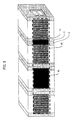
- the LD stack shown in FIG. 5 is constituted by four LD modules 5.
- a rectangle 10 indicated by a thick dotted line represents the smallest rectangle having an area "A" enclosing a whole emitting region of the LD stack.
- a rectangle 11 indicated by a small dotted line represents the smallest rectangle having an area "B" enclosing an emitting region of each LD module.
- the rectangle 10 includes non-emitting regions (dead spaces) 12 formed on side surfaces of the connection plates 3 between the adjacent LD modules and the rectangle 11 does not include the dead space 12.
- the dead space 12 is determined in dependence on thickness of the connection plates 3 and also depth of the concavities 3a formed in the connection plates 3 in the embodiment as shown in FIG. 2. It is necessary to reduce the thickness of the connection plate 3 and/or increase the depth of the concavities 3a in order to reduce the dead space 12.
- N (N ⁇ 2) represents the number of LD modules constituting the LD stack
- A, B represent areas of the rectangles 10 and 11, respectively.
- the laser diodes and the connection plates in the LD stack are arranged such that the above index does not exceed "0.2". Fulfilling this condition, a high density of output power from the emitting surface is secured with small dead spaces to realize a high performance of the LD stack constituted by the LD modules.
- the LD stack is divided into a plurality of LD modules to make assembly of the LD stack easy and prevent leakage of the coolant possibly caused by shortage of pressing pressure on the seal members due to non-uniformity of thickness of the cooling devices. Since the LD modules are mechanically and electrically connected with each other in series including the flow passages of the coolant, the connected LD stack can be treated as a module.
- the connected LD stack is used as a surface light-emitting device having a length in accordance with a desired length of a solid-state laser medium with small dead spaces.
- the connection plates for connecting the Ld modules also function as fixture for fixedly supporting the cooling devices in the LD module to simplify the structure of the LD module.
- the electrical connection between the LD modules can be made independent while the LD modules are connected mechanically, so that diagnose of deterioration of the LD module can be performed.
- the LD stack is repaired by replacing a LD module containing a broken LD with a new LD module to continuously use the LD modules other than the LD module containing the broken LD.
- the LD stack is used economically. Since an operation for replacing the LD module in the LD stack is easy performed, the maintenance of the LD stack is made easy.
Landscapes
- Physics & Mathematics (AREA)
- Electromagnetism (AREA)
- Optics & Photonics (AREA)
- Condensed Matter Physics & Semiconductors (AREA)
- General Physics & Mathematics (AREA)
- Engineering & Computer Science (AREA)
- Plasma & Fusion (AREA)
- Lasers (AREA)
- Semiconductor Lasers (AREA)
Applications Claiming Priority (2)
| Application Number | Priority Date | Filing Date | Title |
|---|---|---|---|
| JP2001223223 | 2001-07-24 | ||
| JP2001223223A JP3830364B2 (ja) | 2001-07-24 | 2001-07-24 | 固体レーザ励起用光源装置 |
Publications (3)
| Publication Number | Publication Date |
|---|---|
| EP1284527A2 true EP1284527A2 (fr) | 2003-02-19 |
| EP1284527A3 EP1284527A3 (fr) | 2004-03-03 |
| EP1284527B1 EP1284527B1 (fr) | 2006-02-15 |
Family
ID=19056591
Family Applications (1)
| Application Number | Title | Priority Date | Filing Date |
|---|---|---|---|
| EP02255148A Expired - Lifetime EP1284527B1 (fr) | 2001-07-24 | 2002-07-23 | Dispositif source de lumière pour le pompage d'un laser à l'état solide |
Country Status (4)
| Country | Link |
|---|---|
| US (1) | US6850549B2 (fr) |
| EP (1) | EP1284527B1 (fr) |
| JP (1) | JP3830364B2 (fr) |
| DE (1) | DE60209186T2 (fr) |
Cited By (1)
| Publication number | Priority date | Publication date | Assignee | Title |
|---|---|---|---|---|
| WO2005067112A1 (fr) * | 2003-12-31 | 2005-07-21 | The Boeing Company | Laser solide comprenant des diodes hermetiquement scellees |
Families Citing this family (6)
| Publication number | Priority date | Publication date | Assignee | Title |
|---|---|---|---|---|
| KR20050091915A (ko) * | 2004-03-11 | 2005-09-16 | 주식회사 솔고 바이오메디칼 | 반도체 레이저 다이오드 바 스택 방법 |
| EP2050145A4 (fr) * | 2006-07-28 | 2009-09-02 | Koninkl Philips Electronics Nv | Source de lumiere comprenant des elements d'emission marginale |
| JP5611334B2 (ja) | 2009-08-31 | 2014-10-22 | 西安炬光科技有限公司 | レーザ用冷却モジュール、製造方法および該モジュールで製造した半導体レーザ |
| US8989226B2 (en) * | 2009-08-31 | 2015-03-24 | Xi'an Focuslight Technologies Co., Ltd. | Cooling module for laser, fabricating method thereof, and semiconductor laser fabricated from the module |
| JP5729107B2 (ja) | 2011-04-20 | 2015-06-03 | 村田機械株式会社 | レーザ発振器制御装置 |
| US10170893B1 (en) * | 2017-08-09 | 2019-01-01 | Waymo Llc | Vacuum fixture |
Family Cites Families (14)
| Publication number | Priority date | Publication date | Assignee | Title |
|---|---|---|---|---|
| US5105429A (en) * | 1990-07-06 | 1992-04-14 | The United States Of America As Represented By The Department Of Energy | Modular package for cooling a laser diode array |
| US5311530A (en) * | 1990-09-14 | 1994-05-10 | Advanced Optoelectronics, Inc. | Semiconductor laser array |
| US5105430A (en) * | 1991-04-09 | 1992-04-14 | The United States Of America As Represented By The United States Department Of Energy | Thin planar package for cooling an array of edge-emitting laser diodes |
| JPH07202332A (ja) | 1993-12-28 | 1995-08-04 | Fuji Electric Co Ltd | 半導体レーザ素子および固体レーザ装置 |
| US5495490A (en) * | 1995-02-28 | 1996-02-27 | Mcdonnell Douglas Corporation | Immersion method and apparatus for cooling a semiconductor laser device |
| FR2741208B1 (fr) * | 1995-11-13 | 1997-12-05 | Commissariat Energie Atomique | Assemblage de barrettes de diodes laser refroidies |
| JPH09181376A (ja) | 1995-12-26 | 1997-07-11 | Mitsubishi Heavy Ind Ltd | 固体レーザ励起用半導体レーザ及びその製造方法 |
| JP3816194B2 (ja) | 1996-11-22 | 2006-08-30 | ファナック株式会社 | 冷却装置、光源装置、面発光装置、およびその製造方法 |
| US5815523A (en) * | 1996-11-27 | 1998-09-29 | Mcdonnell Douglas Corporation | Variable power helix laser amplifier and laser |
| US6151341A (en) * | 1997-05-30 | 2000-11-21 | Excel/Quantronix, Inc. | Stackable integrated diode packaging |
| DE69931937T2 (de) | 1998-08-18 | 2007-02-15 | Hamamatsu Photonics K.K., Hamamatsu | Kühlkörper, halbleiterlaser und halbleiterlaserstapel mit diesem kühlkörper |
| JP3681581B2 (ja) * | 1999-07-30 | 2005-08-10 | ファナック株式会社 | 冷却装置とそれを備えた面発光装置 |
| JP4031903B2 (ja) * | 1999-10-21 | 2008-01-09 | イェーノプティク アクチエンゲゼルシャフト | ダイオードレーザを冷却する装置 |
| JP3473540B2 (ja) * | 2000-02-23 | 2003-12-08 | 日本電気株式会社 | 半導体レーザの冷却装置 |
-
2001
- 2001-07-24 JP JP2001223223A patent/JP3830364B2/ja not_active Expired - Fee Related
-
2002
- 2002-07-23 DE DE60209186T patent/DE60209186T2/de not_active Expired - Fee Related
- 2002-07-23 EP EP02255148A patent/EP1284527B1/fr not_active Expired - Lifetime
- 2002-07-24 US US10/200,756 patent/US6850549B2/en not_active Expired - Fee Related
Cited By (1)
| Publication number | Priority date | Publication date | Assignee | Title |
|---|---|---|---|---|
| WO2005067112A1 (fr) * | 2003-12-31 | 2005-07-21 | The Boeing Company | Laser solide comprenant des diodes hermetiquement scellees |
Also Published As
| Publication number | Publication date |
|---|---|
| EP1284527B1 (fr) | 2006-02-15 |
| US20030031227A1 (en) | 2003-02-13 |
| DE60209186D1 (de) | 2006-04-20 |
| JP2003037316A (ja) | 2003-02-07 |
| US6850549B2 (en) | 2005-02-01 |
| EP1284527A3 (fr) | 2004-03-03 |
| JP3830364B2 (ja) | 2006-10-04 |
| DE60209186T2 (de) | 2006-07-20 |
Similar Documents
| Publication | Publication Date | Title |
|---|---|---|
| US9029814B2 (en) | LED light source device | |
| CN114243451B (zh) | 半导体泵浦源及光纤激光器 | |
| US6850549B2 (en) | Light source device for pumping solid-state laser medium | |
| US7113528B2 (en) | Semiconductor laser device | |
| US7271419B2 (en) | Laser device having a plurality of emission zones | |
| WO2021256421A1 (fr) | Dispositif électroluminescent à semi-conducteur et appareil électroluminescent le comprenant | |
| CN111048989A (zh) | 光纤耦合输出半导体激光器 | |
| CN117458263A (zh) | 一种半导体激光器芯片及高功率半导体激光器叠阵模块 | |
| CA3191466A1 (fr) | Assemblage de diode laser de puissance a pic eleve | |
| CN215070862U (zh) | 一种激光脱毛半导体激光模组 | |
| CN116093744A (zh) | 一种基于波长合束与偏振合束的双波长激光合束装置 | |
| CN212412421U (zh) | 一种集成化小体积yag脉冲光纤焊接激光器 | |
| CN223967505U (zh) | 一种阵列激光发射装置 | |
| CN210954612U (zh) | 一种激光直写曝光机的激光器及激光直写曝光机 | |
| CN224082917U (zh) | 一种用于光纤激光器的水冷板 | |
| CN114051669A (zh) | 电池模块及其制造方法 | |
| CN112202038A (zh) | 一种集成化小体积yag脉冲光纤焊接激光器 | |
| CN119209177B (zh) | 一种可调谐单频脉冲光纤激光器 | |
| CN219105334U (zh) | 一种光源装置以及照明系统 | |
| CN219760242U (zh) | 一种快轴准直半导体激光器阵列 | |
| CN216251620U (zh) | 一种多波长cos阵列激光器 | |
| RU2854621C1 (ru) | Микроканальный лазерный излучатель | |
| CN114937914A (zh) | 一种半导体激光器 | |
| CN219419851U (zh) | 泵浦冷却组件及激光器 | |
| CN223217777U (zh) | 矩阵型白激光灯以及投影装置 |
Legal Events
| Date | Code | Title | Description |
|---|---|---|---|
| PUAI | Public reference made under article 153(3) epc to a published international application that has entered the european phase |
Free format text: ORIGINAL CODE: 0009012 |
|
| AK | Designated contracting states |
Designated state(s): AT BE BG CH CY CZ DE DK EE ES FI FR GB GR IE IT LI LU MC NL PT SE SK TR |
|
| AX | Request for extension of the european patent |
Extension state: AL LT LV MK RO SI |
|
| PUAL | Search report despatched |
Free format text: ORIGINAL CODE: 0009013 |
|
| AK | Designated contracting states |
Kind code of ref document: A3 Designated state(s): AT BE BG CH CY CZ DE DK EE ES FI FR GB GR IE IT LI LU MC NL PT SE SK TR |
|
| AX | Request for extension of the european patent |
Extension state: AL LT LV MK RO SI |
|
| RAP1 | Party data changed (applicant data changed or rights of an application transferred) |
Owner name: FANUC LTD |
|
| 17P | Request for examination filed |
Effective date: 20040705 |
|
| AKX | Designation fees paid |
Designated state(s): DE |
|
| 17Q | First examination report despatched |
Effective date: 20050127 |
|
| GRAP | Despatch of communication of intention to grant a patent |
Free format text: ORIGINAL CODE: EPIDOSNIGR1 |
|
| RIN1 | Information on inventor provided before grant (corrected) |
Inventor name: SATO, MASAO Inventor name: MIYATA, RYUSUKE,FANUC DAI3VIRAKARAMATSU Inventor name: TAKIGAWA, HIROSHI Inventor name: NISHIKAWA, YUJI,FANUC MANSHONHARIMOMI Inventor name: NAITO, SHINYA |
|
| GRAS | Grant fee paid |
Free format text: ORIGINAL CODE: EPIDOSNIGR3 |
|
| GRAA | (expected) grant |
Free format text: ORIGINAL CODE: 0009210 |
|
| AK | Designated contracting states |
Kind code of ref document: B1 Designated state(s): DE |
|
| REF | Corresponds to: |
Ref document number: 60209186 Country of ref document: DE Date of ref document: 20060420 Kind code of ref document: P |
|
| PLBE | No opposition filed within time limit |
Free format text: ORIGINAL CODE: 0009261 |
|
| STAA | Information on the status of an ep patent application or granted ep patent |
Free format text: STATUS: NO OPPOSITION FILED WITHIN TIME LIMIT |
|
| 26N | No opposition filed |
Effective date: 20061116 |
|
| PGFP | Annual fee paid to national office [announced via postgrant information from national office to epo] |
Ref country code: DE Payment date: 20080908 Year of fee payment: 7 |
|
| PG25 | Lapsed in a contracting state [announced via postgrant information from national office to epo] |
Ref country code: DE Free format text: LAPSE BECAUSE OF NON-PAYMENT OF DUE FEES Effective date: 20100202 |