EP1284590A1 - Dispositif de connexion de lignes de raccordement avec un élement de connexion élastique et stratifié - Google Patents
Dispositif de connexion de lignes de raccordement avec un élement de connexion élastique et stratifié Download PDFInfo
- Publication number
- EP1284590A1 EP1284590A1 EP02405656A EP02405656A EP1284590A1 EP 1284590 A1 EP1284590 A1 EP 1284590A1 EP 02405656 A EP02405656 A EP 02405656A EP 02405656 A EP02405656 A EP 02405656A EP 1284590 A1 EP1284590 A1 EP 1284590A1
- Authority
- EP
- European Patent Office
- Prior art keywords
- connection contacts
- zebral
- contacting device
- layers
- depressions
- Prior art date
- Legal status (The legal status is an assumption and is not a legal conclusion. Google has not performed a legal analysis and makes no representation as to the accuracy of the status listed.)
- Withdrawn
Links
Images

Classifications
-
- H—ELECTRICITY
- H01—ELECTRIC ELEMENTS
- H01R—ELECTRICALLY-CONDUCTIVE CONNECTIONS; STRUCTURAL ASSOCIATIONS OF A PLURALITY OF MUTUALLY-INSULATED ELECTRICAL CONNECTING ELEMENTS; COUPLING DEVICES; CURRENT COLLECTORS
- H01R13/00—Details of coupling devices of the kinds covered by groups H01R12/70 or H01R24/00 - H01R33/00
- H01R13/02—Contact members
- H01R13/22—Contacts for co-operating by abutting
- H01R13/24—Contacts for co-operating by abutting resilient; resiliently-mounted
- H01R13/2407—Contacts for co-operating by abutting resilient; resiliently-mounted characterized by the resilient means
- H01R13/2414—Contacts for co-operating by abutting resilient; resiliently-mounted characterized by the resilient means conductive elastomers
-
- H—ELECTRICITY
- H01—ELECTRIC ELEMENTS
- H01R—ELECTRICALLY-CONDUCTIVE CONNECTIONS; STRUCTURAL ASSOCIATIONS OF A PLURALITY OF MUTUALLY-INSULATED ELECTRICAL CONNECTING ELEMENTS; COUPLING DEVICES; CURRENT COLLECTORS
- H01R12/00—Structural associations of a plurality of mutually-insulated electrical connecting elements, specially adapted for printed circuits, e.g. printed circuit boards [PCB], flat or ribbon cables, or like generally planar structures, e.g. terminal strips, terminal blocks; Coupling devices specially adapted for printed circuits, flat or ribbon cables, or like generally planar structures; Terminals specially adapted for contact with, or insertion into, printed circuits, flat or ribbon cables, or like generally planar structures
- H01R12/50—Fixed connections
- H01R12/59—Fixed connections for flexible printed circuits, flat or ribbon cables or like structures
- H01R12/62—Fixed connections for flexible printed circuits, flat or ribbon cables or like structures connecting to rigid printed circuits or like structures
-
- H—ELECTRICITY
- H05—ELECTRIC TECHNIQUES NOT OTHERWISE PROVIDED FOR
- H05K—PRINTED CIRCUITS; CASINGS OR CONSTRUCTIONAL DETAILS OF ELECTRIC APPARATUS; MANUFACTURE OF ASSEMBLAGES OF ELECTRICAL COMPONENTS
- H05K1/00—Printed circuits
- H05K1/02—Details
- H05K1/11—Printed elements for providing electric connections to or between printed circuits
-
- H—ELECTRICITY
- H05—ELECTRIC TECHNIQUES NOT OTHERWISE PROVIDED FOR
- H05K—PRINTED CIRCUITS; CASINGS OR CONSTRUCTIONAL DETAILS OF ELECTRIC APPARATUS; MANUFACTURE OF ASSEMBLAGES OF ELECTRICAL COMPONENTS
- H05K3/00—Apparatus or processes for manufacturing printed circuits
- H05K3/30—Assembling printed circuits with electric components, e.g. with resistors
- H05K3/32—Assembling printed circuits with electric components, e.g. with resistors electrically connecting electric components or wires to printed circuits
- H05K3/325—Assembling printed circuits with electric components, e.g. with resistors electrically connecting electric components or wires to printed circuits by abutting or pinching; Mechanical auxiliary parts therefor
-
- H—ELECTRICITY
- H05—ELECTRIC TECHNIQUES NOT OTHERWISE PROVIDED FOR
- H05K—PRINTED CIRCUITS; CASINGS OR CONSTRUCTIONAL DETAILS OF ELECTRIC APPARATUS; MANUFACTURE OF ASSEMBLAGES OF ELECTRICAL COMPONENTS
- H05K2201/00—Indexing scheme relating to printed circuits covered by H05K1/00
- H05K2201/03—Conductive materials
- H05K2201/0302—Properties and characteristics in general
- H05K2201/0314—Elastomeric connector or conductor, e.g. rubber with metallic filler
-
- H—ELECTRICITY
- H05—ELECTRIC TECHNIQUES NOT OTHERWISE PROVIDED FOR
- H05K—PRINTED CIRCUITS; CASINGS OR CONSTRUCTIONAL DETAILS OF ELECTRIC APPARATUS; MANUFACTURE OF ASSEMBLAGES OF ELECTRICAL COMPONENTS
- H05K2201/00—Indexing scheme relating to printed circuits covered by H05K1/00
- H05K2201/03—Conductive materials
- H05K2201/032—Materials
- H05K2201/0326—Inorganic, non-metallic conductor, e.g. indium-tin oxide [ITO]
-
- H—ELECTRICITY
- H05—ELECTRIC TECHNIQUES NOT OTHERWISE PROVIDED FOR
- H05K—PRINTED CIRCUITS; CASINGS OR CONSTRUCTIONAL DETAILS OF ELECTRIC APPARATUS; MANUFACTURE OF ASSEMBLAGES OF ELECTRICAL COMPONENTS
- H05K2201/00—Indexing scheme relating to printed circuits covered by H05K1/00
- H05K2201/03—Conductive materials
- H05K2201/0332—Structure of the conductor
- H05K2201/0364—Conductor shape
- H05K2201/0373—Conductors having a fine structure, e.g. providing a plurality of contact points with a structured tool
-
- H—ELECTRICITY
- H05—ELECTRIC TECHNIQUES NOT OTHERWISE PROVIDED FOR
- H05K—PRINTED CIRCUITS; CASINGS OR CONSTRUCTIONAL DETAILS OF ELECTRIC APPARATUS; MANUFACTURE OF ASSEMBLAGES OF ELECTRICAL COMPONENTS
- H05K2201/00—Indexing scheme relating to printed circuits covered by H05K1/00
- H05K2201/10—Details of components or other objects attached to or integrated in a printed circuit board
- H05K2201/10007—Types of components
- H05K2201/10128—Display
- H05K2201/10136—Liquid Crystal display [LCD]
Definitions
- the invention relates to a device for contacting Connection lines of electronic modules using a elastic connecting element according to the preamble of Claim 1.
- Such elastic and electrically conductive connecting elements are for example from [1], U.S. Patent No. 5,599,193 and [2], U.S. Patent No. 5,517,752 known.
- connecting elements are described which are non-conductive Have substrate, which on both sides with electrically conductive layers is provided by means of electrical lines are connected so that an electrical connection between contacts of Modules are created on which the electrically conductive layers issue.
- the surfaces are preferably electrically conductive Layers roughened, so that during assembly at most existing oxide layers on the connection contacts, the disturbing contact resistance can be broken up become.
- connection element which consists of elastic, provided with electrically conductive particles Connection material exists, which under during assembly elevated temperature is compressed, making it conductive Particles between associated connector contacts be pressed together.
- the connection contacts are with Furrows provided under the action during assembly external forces completely deformed and with elastic Fastening material filled under the influence of Pressure and heat hardened in the compressed state.
- An electrically conductive layer consists of, for example 60 parts by weight of silicon rubber made of organopolysiloxane rubber, 40 parts by weight of acetylene black, 5 parts by weight Carbon fibers and 3 parts by weight of a hardening agent (see [3], column 7).
- a hardening agent see [3], column 7.
- Carbon fibers often become metal wires or balls used with a precious metal like gold; Silver or are coated with a silver oxide.
- the present invention is therefore based on the object a device for contacting connecting lines to specify electronic modules using a zebra rubber, avoided the described contacting problems become.
- a zebral conductive rubber Contacting device can be created by means of Connection lines, especially when installing according to Manufacturer's guidelines, durable with low and constant contact resistance can be connected to each other.
- connection contacts are one or both Modules are provided with recesses or channels to accommodate them and possibly suitable for draining liquid are that come out of the Zebraleitgummi and contact problems can cause.
- Soiling such as hand cream, added during manufacture or assembly on the contact surfaces can reach.
- the recesses or gutters that are made during manufacture embossed or then by roughening, milling or Cutting the surfaces of the connection contacts incorporated are preferably designed so narrow that the elastic material of the zebraleitgummier after it Compression cannot or only partially occur in it, making them filled and draining fluid would be prevented.
- the gutters or depressions can also be applied by the application of several appropriately designed indium tin oxide layers or by milling or cutting, for example by means of a laser beam.
- channels or channels can be created by a layer, optionally a metal or graphite layer is applied to the contact surface, in the larger one Particles, possibly metal spheres, are incorporated in this way are that the escaping liquid can seep away.
- the channels are preferably transverse to the layers of the Zebraleitgummi arranged so that even conductive layers, located in the edge area of the connection contacts, be connected with these as uninterruptedly as possible and leaked liquid can be drained over a short distance can.
- Liquids that leak out of the zebral conduit and onto it Contact surfaces can form an insulation layer therefore channeled according to the invention with simple measures and derived, with an optimal connection between the ensures conductive layers of the zebral conductive rubber and is constantly maintained.
- Contacting devices according to the invention are particularly advantageous can be used when contacting modules, which are manufactured using chip-on-glass technology and for example with vapor-deposited contacts made of indium tin oxide are provided. By inserting gutters on the otherwise smooth connection contacts become contacting problems avoided.
- zebral gums can be used with Carbon fibers or with optionally with precious metals such as Gold, silver or silver oxide coated beads or Particles made of metal or plastic are provided.
- precious metals such as Gold, silver or silver oxide coated beads or Particles made of metal or plastic are provided.
- Especially Contacting devices according to the invention are advantageous can also be used when choosing higher compression factors.
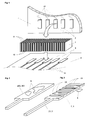
- Figure 1 shows the connection area of two modules 4, 5 with five connection contacts 2 or 3, each using a elastic zebraleitgummi 1 are connected to each other.
- the Zebraleitgummi 1 which is preferably around during assembly at least 10% is compressed alternately interconnected conductive and insulating layers 10, 11 of small diameter. As shown in Figure 3, should correspond to each other after assembly 2, 3 by means of at least two conductive layers 10 be connected.
- the zebral conduction rubber 1 therefore does not have, as in the case of [1] described device, a non-conductive substrate, which is provided on both sides with contact foils through which oxide layers are broken open at high compression can, but continuous conductive layers 10th
- the on the connecting element or the Zebraleitgummi 1 compression force exerted is also much less than in the device described in [2], in which some in Evenly distributed metal particles between the substrate Terminal contacts are pressed into furrows contained therein and thereby the relevant connection contacts with each other connect.
- the COG technology which is the direct connection electronic components with a metallized Glass substrate, is often used to manufacture Liquid crystal displays (LCD) applied (see Mool C. Gupta, Handbook of PHOTONICS, CRC Press LLC, Boca Raton 1997, pages 780-788). Since the preferably made of indium tin oxide Connection contacts 2 of a COG module cannot be soldered these are normally connected by means of a zebra rubber 1.
- Figure 2 shows a conventional smooth connection contact 200, 300, the one with leaked liquid caused insulating layer 8 is covered, which a caused increased contact resistance, due to which the mentioned malfunctions arise.
- FIG. 3 shows a connection contact 2; 3 of the inventive Contacting device according to Figure 1 longer operating time.
- the connection contact 2; 3 is with Provided channels 23, by means of which liquid, which from the Zebraleitgummi 1 leaked, channeled and directed away was, so that a corresponding insulation layer 8 is not on the remaining contact surfaces 24, but next to the Connection contact 2; 3 on the substrate of the associated module 4; 5 was formed.
- the channels 23 are narrow, so the resulting cross-sectional loss is comparatively is small in relation to the cross-sectional loss that otherwise caused by insulation layers 8 leaked liquids can be.
- the channels 23 are preferably designed so narrow that the elastic material of the zebraleitgummi 1 not or only can partially enter this, thereby interrupting the Derivation of, if necessary, from the zebral conductive rubber 1 escaping liquid is prevented.
- the channels 23 are in a preferred embodiment also across the layers 10, 11 of the zebral conductive rubber 1 arranged so that conductive layers 10, which are in the Edge area of the connection contacts 2, 3, if possible are connected to these without interruption and emerging Liquid can be drained over a short distance.
- Troughs 23 are preferably used in the manufacture of the Terminal contacts 2, 3 are stamped into them. It is also possible roughening the surface of the connection contacts 2, 3 after their manufacture.
- the application of the channels or depressions can also be applied by applying several designed indium tin oxide layers or by milling or cutting the surface of the connection contacts 2, 3 for example by means of a laser beam.
- the design of the channels 23 can also be dependent the nature of the Zebraleitgummi 1 done.
Landscapes
- Engineering & Computer Science (AREA)
- Microelectronics & Electronic Packaging (AREA)
- Metallurgy (AREA)
- Manufacturing & Machinery (AREA)
- Liquid Crystal (AREA)
Applications Claiming Priority (2)
| Application Number | Priority Date | Filing Date | Title |
|---|---|---|---|
| CH15002001 | 2001-08-14 | ||
| CH15002001 | 2001-08-14 |
Publications (1)
| Publication Number | Publication Date |
|---|---|
| EP1284590A1 true EP1284590A1 (fr) | 2003-02-19 |
Family
ID=4565524
Family Applications (1)
| Application Number | Title | Priority Date | Filing Date |
|---|---|---|---|
| EP02405656A Withdrawn EP1284590A1 (fr) | 2001-08-14 | 2002-07-28 | Dispositif de connexion de lignes de raccordement avec un élement de connexion élastique et stratifié |
Country Status (1)
| Country | Link |
|---|---|
| EP (1) | EP1284590A1 (fr) |
Cited By (4)
| Publication number | Priority date | Publication date | Assignee | Title |
|---|---|---|---|---|
| WO2005062525A1 (fr) * | 2003-12-22 | 2005-07-07 | Huawei Technologies Co., Ltd. | Procede de traitement du compte rendu des positions provenant d'un equipement utilisateur oriente objet |
| WO2006084971A1 (fr) * | 2005-02-11 | 2006-08-17 | Johnson Controls Technology Company | Connecteur elastomere |
| WO2008152934A1 (fr) | 2007-06-11 | 2008-12-18 | Fuji Polymer Industries Co., Ltd. | Composant en caoutchouc conducteur avec intégration de métal |
| EP2325948A4 (fr) * | 2008-09-16 | 2012-04-04 | Fuji Polymer Ind | Composant électroconducteur en caoutchouc |
Citations (5)
| Publication number | Priority date | Publication date | Assignee | Title |
|---|---|---|---|---|
| JPS58189613A (ja) * | 1982-04-30 | 1983-11-05 | Hitachi Ltd | 液晶表示素子 |
| US4793543A (en) * | 1986-08-28 | 1988-12-27 | Stc Plc | Solder joint |
| JPH0738241A (ja) * | 1993-07-23 | 1995-02-07 | Ricoh Co Ltd | 印刷配線板の電極構造及び形成方法 |
| US5984691A (en) * | 1996-05-24 | 1999-11-16 | International Business Machines Corporation | Flexible circuitized interposer with apertured member and method for making same |
| US6010340A (en) * | 1998-03-04 | 2000-01-04 | Internatinal Business Machines Corporation | Solder column tip compliancy modification for use in a BGA socket connector |
-
2002
- 2002-07-28 EP EP02405656A patent/EP1284590A1/fr not_active Withdrawn
Patent Citations (5)
| Publication number | Priority date | Publication date | Assignee | Title |
|---|---|---|---|---|
| JPS58189613A (ja) * | 1982-04-30 | 1983-11-05 | Hitachi Ltd | 液晶表示素子 |
| US4793543A (en) * | 1986-08-28 | 1988-12-27 | Stc Plc | Solder joint |
| JPH0738241A (ja) * | 1993-07-23 | 1995-02-07 | Ricoh Co Ltd | 印刷配線板の電極構造及び形成方法 |
| US5984691A (en) * | 1996-05-24 | 1999-11-16 | International Business Machines Corporation | Flexible circuitized interposer with apertured member and method for making same |
| US6010340A (en) * | 1998-03-04 | 2000-01-04 | Internatinal Business Machines Corporation | Solder column tip compliancy modification for use in a BGA socket connector |
Non-Patent Citations (2)
| Title |
|---|
| PATENT ABSTRACTS OF JAPAN vol. 008, no. 033 (P - 254) 14 February 1984 (1984-02-14) * |
| PATENT ABSTRACTS OF JAPAN vol. 1995, no. 05 30 June 1995 (1995-06-30) * |
Cited By (7)
| Publication number | Priority date | Publication date | Assignee | Title |
|---|---|---|---|---|
| WO2005062525A1 (fr) * | 2003-12-22 | 2005-07-07 | Huawei Technologies Co., Ltd. | Procede de traitement du compte rendu des positions provenant d'un equipement utilisateur oriente objet |
| WO2006084971A1 (fr) * | 2005-02-11 | 2006-08-17 | Johnson Controls Technology Company | Connecteur elastomere |
| FR2882197A1 (fr) * | 2005-02-11 | 2006-08-18 | Johnson Controls Tech Co | Connecteur elastomere feuillete a test d'ecrasement, et dispositif de connexion comportant un tel connecteur |
| WO2008152934A1 (fr) | 2007-06-11 | 2008-12-18 | Fuji Polymer Industries Co., Ltd. | Composant en caoutchouc conducteur avec intégration de métal |
| EP2073619A4 (fr) * | 2007-06-11 | 2010-10-27 | Fuji Polymer Ind | Composant en caoutchouc conducteur avec integration de metal |
| US7976927B2 (en) | 2007-06-11 | 2011-07-12 | Fuji Polymer Industries Co., Ltd. | Metal-integral conductive rubber component |
| EP2325948A4 (fr) * | 2008-09-16 | 2012-04-04 | Fuji Polymer Ind | Composant électroconducteur en caoutchouc |
Similar Documents
| Publication | Publication Date | Title |
|---|---|---|
| DE69535551T2 (de) | Halbleiteranordnung mit Kontaktlöchern | |
| DE69627389T2 (de) | Leitfähige elastomere und verfahren zur herstellung derselben | |
| DE69736722T2 (de) | Steckverbinder hoher Kontaktdichte | |
| EP0004899B1 (fr) | Procédé pour établir des connexions électriquement conductrices et sans oscillations entre des circuits imprimés sur la surface arrière d'une plaque à circuits et des ressorts de contact des réglettes à ressorts de contact, aussi bien que réglette à ressorts de contact appropriée | |
| DE60218961T2 (de) | Einpress-Sammelschiene für Leistungsversorgung | |
| DE69414686T2 (de) | Elektrische verbindungsstruktur und verfahren zum elektrischen verbinden von anschluessen untereinander | |
| DE112012002406T5 (de) | Dehnbare Schaltungsanordnungen | |
| CH667562A5 (de) | Verfahren zum aendern einer elektrischen flachbaugruppe. | |
| DE10293878T5 (de) | Transparentes Berührungsfeld und Verfahren zur Herstellung des Berührungsfeldes | |
| DE60124977T2 (de) | Elektrisches lötbares Verbindungselement mit Lötstelle | |
| EP0718878A2 (fr) | Procédé de fabrication de conducteurs sur un substrat avec des dépressions | |
| DE102004043464A1 (de) | Schaltungsplatte mit einer Metallplatte, gedruckte Schaltungsplatte und flexible Schaltungsplatine | |
| DE19733877B4 (de) | Über eine Matrix adressierte Anzeigevorrichtung | |
| EP1284590A1 (fr) | Dispositif de connexion de lignes de raccordement avec un élement de connexion élastique et stratifié | |
| DE69019600T2 (de) | Plasma-Anzeigevorrichtung. | |
| DE102004045896A1 (de) | Transponder mit Antenne und Flip-Chip-Modul und Verfahren zu dessen Herstellung | |
| DE19539181C2 (de) | Chipkartenmodul sowie entsprechendes Herstellungsverfahren | |
| EP1940207A2 (fr) | Dispositif électrique doté d'un élément de support ayant au moins une surface de raccordement spécifique et un composant monté sur la surface | |
| DE4319876A1 (de) | Verfahren zum Befestigen einer Hybrid-Schaltung auf einer Leiterplatte | |
| DE69810575T2 (de) | Elektrolumineszentes Element | |
| DE10059808A1 (de) | Verfahren zur Verbindung einer integrierten Schaltung und einer flexiblen Schaltung | |
| DE3211408A1 (de) | Substrat | |
| DE102011004543B4 (de) | Widerstand, Leiterplatte und elektrisches oder elektronisches Gerät | |
| WO2007012514A1 (fr) | Connexion electroconductrice et procede de production de cette connexion | |
| EP1162694B1 (fr) | Appareil pour la connexion de conducteurs électriques |
Legal Events
| Date | Code | Title | Description |
|---|---|---|---|
| PUAI | Public reference made under article 153(3) epc to a published international application that has entered the european phase |
Free format text: ORIGINAL CODE: 0009012 |
|
| AK | Designated contracting states |
Designated state(s): AT BE BG CH CY CZ DE DK EE ES FI FR GB GR IE IT LI LU MC NL PT SE SK TR |
|
| AX | Request for extension of the european patent |
Extension state: AL LT LV MK RO SI |
|
| AKX | Designation fees paid | ||
| REG | Reference to a national code |
Ref country code: DE Ref legal event code: 8566 |
|
| STAA | Information on the status of an ep patent application or granted ep patent |
Free format text: STATUS: THE APPLICATION IS DEEMED TO BE WITHDRAWN |
|
| 18D | Application deemed to be withdrawn |
Effective date: 20030820 |