EP1286202A1 - Unite d'affichage a cristaux liquides et procede d'attaque de ce dernier - Google Patents
Unite d'affichage a cristaux liquides et procede d'attaque de ce dernier Download PDFInfo
- Publication number
- EP1286202A1 EP1286202A1 EP02710455A EP02710455A EP1286202A1 EP 1286202 A1 EP1286202 A1 EP 1286202A1 EP 02710455 A EP02710455 A EP 02710455A EP 02710455 A EP02710455 A EP 02710455A EP 1286202 A1 EP1286202 A1 EP 1286202A1
- Authority
- EP
- European Patent Office
- Prior art keywords
- image signal
- signal
- picture
- liquid crystal
- written
- Prior art date
- Legal status (The legal status is an assumption and is not a legal conclusion. Google has not performed a legal analysis and makes no representation as to the accuracy of the status listed.)
- Withdrawn
Links
Images












Classifications
-
- G—PHYSICS
- G02—OPTICS
- G02F—OPTICAL DEVICES OR ARRANGEMENTS FOR THE CONTROL OF LIGHT BY MODIFICATION OF THE OPTICAL PROPERTIES OF THE MEDIA OF THE ELEMENTS INVOLVED THEREIN; NON-LINEAR OPTICS; FREQUENCY-CHANGING OF LIGHT; OPTICAL LOGIC ELEMENTS; OPTICAL ANALOGUE/DIGITAL CONVERTERS
- G02F1/00—Devices or arrangements for the control of the intensity, colour, phase, polarisation or direction of light arriving from an independent light source, e.g. switching, gating or modulating; Non-linear optics
- G02F1/01—Devices or arrangements for the control of the intensity, colour, phase, polarisation or direction of light arriving from an independent light source, e.g. switching, gating or modulating; Non-linear optics for the control of the intensity, phase, polarisation or colour
- G02F1/13—Devices or arrangements for the control of the intensity, colour, phase, polarisation or direction of light arriving from an independent light source, e.g. switching, gating or modulating; Non-linear optics for the control of the intensity, phase, polarisation or colour based on liquid crystals, e.g. single liquid crystal display cells
- G02F1/133—Constructional arrangements; Operation of liquid crystal cells; Circuit arrangements
-
- G—PHYSICS
- G09—EDUCATION; CRYPTOGRAPHY; DISPLAY; ADVERTISING; SEALS
- G09G—ARRANGEMENTS OR CIRCUITS FOR CONTROL OF INDICATING DEVICES USING STATIC MEANS TO PRESENT VARIABLE INFORMATION
- G09G3/00—Control arrangements or circuits, of interest only in connection with visual indicators other than cathode-ray tubes
- G09G3/20—Control arrangements or circuits, of interest only in connection with visual indicators other than cathode-ray tubes for presentation of an assembly of a number of characters, e.g. a page, by composing the assembly by combination of individual elements arranged in a matrix no fixed position being assigned to or needed to be assigned to the individual characters or partial characters
- G09G3/34—Control arrangements or circuits, of interest only in connection with visual indicators other than cathode-ray tubes for presentation of an assembly of a number of characters, e.g. a page, by composing the assembly by combination of individual elements arranged in a matrix no fixed position being assigned to or needed to be assigned to the individual characters or partial characters by control of light from an independent source
- G09G3/36—Control arrangements or circuits, of interest only in connection with visual indicators other than cathode-ray tubes for presentation of an assembly of a number of characters, e.g. a page, by composing the assembly by combination of individual elements arranged in a matrix no fixed position being assigned to or needed to be assigned to the individual characters or partial characters by control of light from an independent source using liquid crystals
- G09G3/3611—Control of matrices with row and column drivers
- G09G3/3648—Control of matrices with row and column drivers using an active matrix
-
- G—PHYSICS
- G09—EDUCATION; CRYPTOGRAPHY; DISPLAY; ADVERTISING; SEALS
- G09G—ARRANGEMENTS OR CIRCUITS FOR CONTROL OF INDICATING DEVICES USING STATIC MEANS TO PRESENT VARIABLE INFORMATION
- G09G2300/00—Aspects of the constitution of display devices
- G09G2300/04—Structural and physical details of display devices
- G09G2300/0469—Details of the physics of pixel operation
- G09G2300/0478—Details of the physics of pixel operation related to liquid crystal pixels
- G09G2300/0491—Use of a bi-refringent liquid crystal, optically controlled bi-refringence [OCB] with bend and splay states, or electrically controlled bi-refringence [ECB] for controlling the color
-
- G—PHYSICS
- G09—EDUCATION; CRYPTOGRAPHY; DISPLAY; ADVERTISING; SEALS
- G09G—ARRANGEMENTS OR CIRCUITS FOR CONTROL OF INDICATING DEVICES USING STATIC MEANS TO PRESENT VARIABLE INFORMATION
- G09G2310/00—Command of the display device
- G09G2310/02—Addressing, scanning or driving the display screen or processing steps related thereto
- G09G2310/0243—Details of the generation of driving signals
- G09G2310/0251—Precharge or discharge of pixel before applying new pixel voltage
-
- G—PHYSICS
- G09—EDUCATION; CRYPTOGRAPHY; DISPLAY; ADVERTISING; SEALS
- G09G—ARRANGEMENTS OR CIRCUITS FOR CONTROL OF INDICATING DEVICES USING STATIC MEANS TO PRESENT VARIABLE INFORMATION
- G09G2310/00—Command of the display device
- G09G2310/06—Details of flat display driving waveforms
-
- G—PHYSICS
- G09—EDUCATION; CRYPTOGRAPHY; DISPLAY; ADVERTISING; SEALS
- G09G—ARRANGEMENTS OR CIRCUITS FOR CONTROL OF INDICATING DEVICES USING STATIC MEANS TO PRESENT VARIABLE INFORMATION
- G09G2320/00—Control of display operating conditions
- G09G2320/02—Improving the quality of display appearance
- G09G2320/0209—Crosstalk reduction, i.e. to reduce direct or indirect influences of signals directed to a certain pixel of the displayed image on other pixels of said image, inclusive of influences affecting pixels in different frames or fields or sub-images which constitute a same image, e.g. left and right images of a stereoscopic display
-
- G—PHYSICS
- G09—EDUCATION; CRYPTOGRAPHY; DISPLAY; ADVERTISING; SEALS
- G09G—ARRANGEMENTS OR CIRCUITS FOR CONTROL OF INDICATING DEVICES USING STATIC MEANS TO PRESENT VARIABLE INFORMATION
- G09G3/00—Control arrangements or circuits, of interest only in connection with visual indicators other than cathode-ray tubes
- G09G3/20—Control arrangements or circuits, of interest only in connection with visual indicators other than cathode-ray tubes for presentation of an assembly of a number of characters, e.g. a page, by composing the assembly by combination of individual elements arranged in a matrix no fixed position being assigned to or needed to be assigned to the individual characters or partial characters
- G09G3/34—Control arrangements or circuits, of interest only in connection with visual indicators other than cathode-ray tubes for presentation of an assembly of a number of characters, e.g. a page, by composing the assembly by combination of individual elements arranged in a matrix no fixed position being assigned to or needed to be assigned to the individual characters or partial characters by control of light from an independent source
- G09G3/36—Control arrangements or circuits, of interest only in connection with visual indicators other than cathode-ray tubes for presentation of an assembly of a number of characters, e.g. a page, by composing the assembly by combination of individual elements arranged in a matrix no fixed position being assigned to or needed to be assigned to the individual characters or partial characters by control of light from an independent source using liquid crystals
- G09G3/3611—Control of matrices with row and column drivers
- G09G3/3614—Control of polarity reversal in general
-
- G—PHYSICS
- G09—EDUCATION; CRYPTOGRAPHY; DISPLAY; ADVERTISING; SEALS
- G09G—ARRANGEMENTS OR CIRCUITS FOR CONTROL OF INDICATING DEVICES USING STATIC MEANS TO PRESENT VARIABLE INFORMATION
- G09G3/00—Control arrangements or circuits, of interest only in connection with visual indicators other than cathode-ray tubes
- G09G3/20—Control arrangements or circuits, of interest only in connection with visual indicators other than cathode-ray tubes for presentation of an assembly of a number of characters, e.g. a page, by composing the assembly by combination of individual elements arranged in a matrix no fixed position being assigned to or needed to be assigned to the individual characters or partial characters
- G09G3/34—Control arrangements or circuits, of interest only in connection with visual indicators other than cathode-ray tubes for presentation of an assembly of a number of characters, e.g. a page, by composing the assembly by combination of individual elements arranged in a matrix no fixed position being assigned to or needed to be assigned to the individual characters or partial characters by control of light from an independent source
- G09G3/36—Control arrangements or circuits, of interest only in connection with visual indicators other than cathode-ray tubes for presentation of an assembly of a number of characters, e.g. a page, by composing the assembly by combination of individual elements arranged in a matrix no fixed position being assigned to or needed to be assigned to the individual characters or partial characters by control of light from an independent source using liquid crystals
- G09G3/3611—Control of matrices with row and column drivers
- G09G3/3648—Control of matrices with row and column drivers using an active matrix
- G09G3/3655—Details of drivers for counter electrodes, e.g. common electrodes for pixel capacitors or supplementary storage capacitors
Definitions
- the present invention relates to liquid crystal devices, more specifically, relates to a liquid crystal device using an active-matrix-type liquid crystal panel, and can be expediently applied to a liquid crystal device in OCB (Optically self-Compensated Birefringence) mode.
- OCB Optically self-Compensated Birefringence
- liquid crystal devices have been used as a screen display device for a computer device, and are expected to be used more in the future also for TVs.
- liquid crystal display devices are those in TN (Twisted Nematic) mode, having a narrow viewing angle and an insufficient response rate. This causes problems such as reduction in contrast due to parallax and blurs in moving pictures, posing a large problem about the display capability in TN mode for TVs.
- TN Transmission Nematic
- the OCB mode is a scheme with a wide viewing angle and a high-speed response compared with the TN mode. Therefore, the OCB mode is a display mode more suitable for nature motion picture display.
- liquid crystal display device and a method of driving the same that adopt the OCB mode.
- FIG. 1 illustrates the construction of a conventional liquid crystal display device.
- the liquid crystal display device includes gate lines GL1 through GLn, source lines SL1 through SLm, a plurality of thin-film transistors (hereinafter referred to as TFTs) 103 as switching devices, etc.
- FIG. 2 illustrates a picture element section thereof.
- a drain electrode of the TFT 103 is connected to a picture-element electrode in a picture element 104.
- the picture element 104 is structured by the picture-element electrode, a common electrode 201, a liquid crystal 202 held between both of these electrodes, and a storage capacitor 203 formed between the picture-element electrode and the common electrode 201.
- the common electrode 201 is driven by a voltage supplied by a common driving section 105 illustrated in FIG. 1.
- the gate driver 101 applies a voltage to the gate lines GL1 through GLn for turning the TFTs 103 ON or OFF. In synchronization with data supply to the source lines SL1 through SLm, the gate driver 101 sequentially applies an ON potential to the gate lines GL1 through GLn.
- the source driver 102 applies a voltage to the source lines SL1 through SLm to supply the voltage to the respective picture elements 104.
- a difference between the voltage supplied to the common electrode 201 and the voltage supplied to each of the source lines SL1 through SLm to be applied to the picture element 104 is a voltage between both ends of the liquid crystal 202 in the picture element 104. This voltage determines the transmittance of the picture element 104.
- the above driving scheme is applied not only to OCB cells but also to a case where TN-type cells are used.
- an activation step of starting video display requires unique driving, which is not required when the TN-type cells are used.
- An OCB cell has a bend configuration enabling image display or a spray configuration disabling imaged display.
- transition To cause transition from the spray configuration to the bend configuration (hereinafter referred to as transition), the unique driving is required, such as applying a high voltage for a predetermined time. Note that the driving associated with transition is not directly related to the present invention, and therefore is not further described herein.
- This OCB cell has a problem that, even once transition is made to the bend configuration by the above unique driving, if a voltage over a predetermined level has not been applied for over a predetermined time, the bend configuration cannot be maintained and is back to the spray configuration. This phenomenon is hereinafter called "back transition”.
- FIG.3 illustrates potential-transmittance curves observed in general OCB.
- a curve 301 is a potential-transmittance curve at normal driving, not at anti-back transition driving, and a curve 302 is a potential-transmittance curve at anti-back transition driving.
- a potential 303 indicates a critical potential Vth at which back transition occurs at normal driving.
- a potential 304 is a potential when the transmittance is at the highest (white potential), and a potential 305 is a potential when the transmittance is at the lowest (black potential).
- the configuration of the OCB cell is back to the spray configuration when the potential becomes Vth or lower, and therefore an appropriate transmittance cannot be obtained.
- driving is always made with a potential not lower than Vth. In such case, however, as illustrated in FIG. 3, sufficient luminance cannot be obtained. For this reason, the OCB requires anti-back transition driving to be carried out.
- liquid crystals typified by OCB and TN require so-called alternating driving to be carried out.
- alternating driving the above-described Japanese Patent Laid-Open Publication No. 11-109921 and Japanese Liquid Crystal Society Journal do not disclose any specific construction of a liquid crystal display device in OCB mode. Therefore, both of the documents do not help specify which type of alternate inversion should be carried out. Therefore, hereinafter described is a virtual example of anti-back transition driving when the most general alternating driving (that is, a combination of line-by-line inversion and frame-by-frame inversion) is carried out.
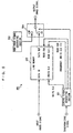
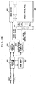
- FIG. 4 is an illustration showing the construction of a liquid crystal display device as the virtual example.
- the liquid crystal display device includes a signal converting section 401, a driving pulse generating section 402, a source driver 403, a gate driver 404, and a liquid crystal panel 405.
- the signal converting section 401 doubles the speed of an input image signal line by line, converting it into a double-speed signal composed of a double-speed image signal and a double-speed non-image signal.
- the driving pulse generating section 402 generates pulses for driving the respective drivers 403 and 404.
- the number of source lines of the liquid crystal panel 405 is ten (SL1 through SL10)
- the number of gate lines is ten (GL1 through GL10)
- one frame period is composed of ten horizontal periods.
- An input image signal is doubled in speed line by line in the signal converting section 401, and is then supplied to the source driver 403.
- FIG. 5 illustrates a specific construction of the signal converting section 401.
- FIG. 6 illustrates timing of a converting operation.
- the control signal generating section 501 generates various control signals, such as a clock, from a synchronizing signal synchronized with the input image signal.
- the input image signal is written in a line memory 502 in synchronization with a write clock from a control signal generating section 501.
- the image signal written in the line memory 502 is read from the line memory 502 in synchronization with a read clock (having a frequency twice as much as that of the write clock) from the control signal generating section 501, and this reading is carried out during a period half of that of writing.
- a read clock having a frequency twice as much as that of the write clock
- the output signal selecting section 504 selects this image signal as an output and, during the remaining period, selects a non-image signal outputted from the non-image signal generating section 503 as an output. Consequently, as illustrated in FIG. 6, in one horizontal period of the input signal, the double-speed non-image signal and image signal are outputted in time sequence.
- the non-image signal is a signal for applying a predetermined high potential to the OCB cells with predetermined periodicity.
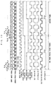
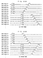
- FIG. 7 is an illustration showing timing of a polarity control signal and driver driving pulses when line-by-line inversion and frame-by-frame inversion are combined as described above.
- the polarity control signal which is to switch alternating polarity, is a signal obtained by XORing a frame inverting signal (A) and a line inverting signal (B), and is generated by the driving pulse generating section 402 illustrated in FIG. 4.
- FIG. 8 An input-output characteristic of the source driver 403 is illustrated in FIG. 8.
- signal outputs higher with respect to a reference potential are illustrated as having a positive polarity, and those lower with respect thereto as having a negative polarity.
- this polarity is represented as "+” or "-" in each gate-selected period.
- "+” is indicated on a gate pulse P1 at a location corresponding to a period T0_1 during which the gate pulse P1 is selected. This indicates that a voltage supplied by the source driver 403 during the period T0_1 has a positive polarity.
- the source driver 403 supplies a positive voltage when the polarity control signal is HI, and supplies a negative voltage when LOW.
- gate pulses P1 through P10 are pulses for selecting ten gate lines (GL1 through GL10), respectively, on the liquid crystal panel 405 during their HI periods.
- the gate pulses P1 through P10 are driven in the following manner in accordance with timing of the double-speed signal inputted to the source driver 403.
- the gate pulse P1 becomes HI, and a positive image signal S1 is written in picture elements on the gate line GL1.
- the gate pulse P7 becomes HI, and a negative non-image signal is written in picture elements on the gate line GL7.
- the gate pulse P2 becomes HI, and a negative image signal S2 is written in picture elements on the gate line GL2.
- the gate pulse P8 becomes HI, and a positive non-image signal is written in picture elements on the gate line GL8. Thereafter, signals are sequentially written in accordance with the polarity of the polarity control signal.
- each of the gate lines (GL1 through GL10) on the liquid crystal panel 405 is selected twice during one frame period.
- an image signal and a non-image signal are written once.
- the gate pulse P1 becomes HI, and a negative image signal S'1, which is opposite in polarity of the signal in the first frame, is written in the picture elements on the gate line GL1.
- the gate pulse P7 becomes HI, and a positive non-image signal, which is opposite in polarity of the signal in the first frame, is written on the gate line GL7. Thereafter, similarly, signals opposite in polarity to those in the first frame are sequentially written.
- the image signal is made opposite in polarity to that in the previous frame so as to avoid sticking caused on the liquid crystal panel when signals of the same polarity are retained for a long time.
- the driving frequency in the above virtual example becomes double. Therefore, the time allocated for writing the image signal to each picture element is shortened by half compared with normal driving. Consequently, writing of data to the picture elements may not sufficiently be carried out.
- an object of the present invention is to provide a liquid crystal display device and a method of driving the same that can suppress the occurrence of back transition without causing the above problems when OCB cells are used and, as a result, can display a good image.
- the present invention has the following aspects.
- a first aspect of the present invention is directed to a liquid crystal display device that displays an image by driving, based on an input image signal, a liquid crystal panel having a plurality of source lines supplied with a picture-element signal, a plurality of gate lines supplied with a scanning signal, and a plurality of picture-element cells arranged in matrix on intersections of the source lines and the gate lines, including: a source driver for supplying the picture-element signal to the source lines; a gate driver for supplying the scanning signal to the gate lines; driving control means for generating a polarity control signal for controlling a polarity of a voltage applied to each of the picture-element cells, and controlling the source driver by the polarity control signal; and a signal converting section for speeding up a transfer rate of the input image signal, and inserting a non-image signal in space of the input image signal, the non-image signal for applying a predetermined voltage to the liquid-crystal cells, to supply the picture-element signal to the source driver, wherein the input
- a second aspect of the present invention is directed to a liquid crystal display device that displays an image by driving, based on an input image signal, a liquid crystal panel having a plurality of source lines supplied with a picture-element signal, a plurality of gate lines supplied with a scanning signal, and a plurality of picture-element cells arranged in matrix on intersections of the source lines and the gate lines, including: a source driver for supplying the picture-element signal to the source lines; a gate driver for supplying the scanning signal to the gate lines; driving control means for generating a polarity control signal for controlling a polarity of a voltage applied to each of the picture-element cells, and controlling the source driver by the polarity control signal; and a signal converting section for speeding up a transfer rate of the input image signal, and inserting a non-image signal in space of the input image signal, the image signal for applying a predetermined voltage to the liquid-crystal cells, to supply the picture-element signal to the source driver, wherein the input image signal
- an input image signal and a non-image signal are sequentially written in the picture-element cells, thereby improving image quality of the moving pictures. Also, the polarity inversion can be balanced, thereby enabling image display evenly.
- the picture-element cells are OCB cells
- the predetermined voltage to be applied to the liquid crystal is a voltage that can prevent a back transition phenomenon of the OCB cells.
- a non-image signal equal in polarity to the input image signal is preliminarily written in the picture-element cell.
- a non-image signal equal in polarity to the non-image signal is further auxiliarily written in the picture-element cell.
- an input image signal equal in polarity to the non-image signal is further preliminarily written.
- writing of the non-image signal becomes easy.
- a seventh aspect of the present invention is directed to a liquid crystal display device that displays an image by driving, based on an input image signal, a liquid crystal panel having a plurality of source lines supplied with a picture-element signal, a plurality of gate lines supplied with a scanning signal, and a plurality of picture-element cells arranged in matrix on intersections of the source lines and the gate lines, including: a source driver for supplying the picture-element signal to the source lines; a gate driver for supplying the scanning signal to the gate lines; and a signal converting section for speeding up a transfer rate of the input image signal, and inserting a non-image signal in space of the input image signal, the non-image signal for applying a predetermined voltage to the liquid-crystal cells, to supply the picture-element signal to the source driver, wherein the non-image signal is written simultaneously to two or more scanning lines corresponding to two or more of the gate lines.
- an input image signal and a non-image signal are sequentially written in the picture-element cells, thereby improving image quality of the moving pictures. Also, it is not required to convert the signal transfer rate to up to a doubled one. Therefore, writing of signals in the picture-element cells become easy.
- the predetermined voltage to be applied to the liquid crystal is a voltage that can prevent a back transfer phenomenon of the OCB cells.
- the liquid crystal display device further includes adjusting means for adjusting the input image signal so that the number of scanning lines to be scanned for one frame period becomes N ⁇ (2M + 1), where the number of the two or more scanning lines in which the non-image signal is simultaneously written is N.
- the number of scanning lines of the input image signal can be adjusted, even when not satisfying a predetermined condition. Therefore, irrespectively of the number of scanning lines of the input image signal, image display can be made more evenly.
- the liquid crystal display device further includes luminance correcting means for correcting luminance of the input image signal at a predetermined degree so that luminance variations due to difference in time periods of retaining the non-image signal for each of the picture-element cells are eliminated.
- luminance variations can be prevented by correcting the luminance.
- the liquid crystal display device further includes rearranging means for rearranging a transfer order of the input image signal so that time periods of retaining the non-image signal for each of the picture-element cells are equal at least for two frame periods, wherein the gate driver supplies a scanning signal corresponding to the rearrangement result by the rearranging means to the gate lines.
- the average insertion time of the non-imagine signal in each scanning line is made evenly, thereby preventing luminance variations from being perceived.
- the liquid crystal display device further includes rearranging means for rearranging a transfer order of the input image signal so that a difference in time period of retaining the non-image signal becomes small between the picture-element cells adjacent to each other, wherein the gate driver supplies a scanning signal corresponding to the rearrangement result by the rearranging means to the gate lines.
- discontinuity in retaining time of the non-image signal among the scanning lines can be resolved. Therefore, it is possible to prevent luminance variations from being perceived.
- the time period of retaining the non-image signal for one frame is arbitrarily adjustable by a user.
- the retaining time of the non-image signal can be arbitrarily adjusted by the user. Therefore, image display according to user's preferences can be made.
- a fourteenth aspect of the present invention is directed to a liquid crystal display device that displays an image by driving, based on an input image signal, a liquid crystal panel having a plurality of source lines supplied with a picture-element signal, a plurality of gate lines supplied with a scanning signal, and a plurality of picture-element cells arranged in matrix on intersections of the source lines and the gate lines, including: each of the picture-element cells including: a transistor connected to the source line and the gate line; a liquid crystal and a storage capacitor respectively connected to the transistor; a common electrode for applying a potential to the liquid crystal; and an other-end electrode for applying a potential to the storage capacitor from a side opposite to a side connected to the transistor, wherein the other-end electrode is given a potential for applying a predetermined voltage to the liquid crystal for a predetermined time period for one frame.
- the predetermined voltage can be applied to the liquid crystal without affecting writing of the input image signal. Therefore, image quality of the moving pictures can be improved without causing problems such as image deterioration due to insufficient recharging of the image signal or processing load on the circuits due to speed-up of the driving frequency.
- the picture-element cells are OCB cells
- the predetermined voltage to be applied to the liquid crystal is a voltage that can prevent a back transition phenomenon of the OCB cells.
- the liquid crystal display device further includes a driver for controlling the potential to be given to the other-end electrode.
- a desired potential can be freely applied to the other-end electrode.
- the other-end electrode is connected to the gate line of another picture-element cell adjacent to the picture-element cell including the other-end electrode, and the other-end electrode is given the potential through the gate line.
- a range of change in a potential from the source line to the picture-element cell is not less than one-fold and less than two-fold of a range of change required for changing a transmittance of the picture-element cell at maximum, and the other-end electrode is further given with a potential for changing a polarity of the voltage to be applied to the picture-element cell.
- a nineteenth aspect of the present invention is directed to a method of driving a liquid crystal display device that displays an image by driving, based on an input image signal, a liquid crystal panel having a plurality of source lines supplied with a picture-element signal, a plurality of gate lines supplied with a scanning signal, and a plurality of picture-element cells arranged in matrix on intersections of the source lines and the gate lines, the method including: a driver controlling step of generating a polarity control signal for controlling a polarity of a voltage to be applied to each of the picture-element cells, and controlling the source driver by the polarity control signal; a step of speeding up a transfer rate of the input image signal; a step of inserting a non-image signal for applying a predetermined voltage to the liquid-crystal cells in space of the input image signal speeded up in the transfer rate; a step of supplying the input image signal speeded up in the transfer rate and having the non-image signal inserted therein to the source line as a picture-
- a twentieth aspect of the present invention is directed to a method of driving a liquid crystal display device that displays an image by driving, based on an input image signal, a liquid crystal panel having a plurality of source lines supplied with a picture-element signal, a plurality of gate lines supplied with a scanning signal, and a plurality of picture-element cells arranged in matrix on intersections of the source lines and the gate lines, the method including: a driver controlling step of generating a polarity control signal for controlling a polarity of a voltage to be applied to each of the picture-element cells, and controlling the source driver by the polarity control signal; a step of speeding up a transfer rate of the input image signal; a step of inserting a non-image signal for applying a predetermined voltage to the liquid-crystal cells in space of the input image signal speeded up in the transfer rate; a step of supplying the input image signal speeded up in the transfer rate and having the non-image signal inserted therein to the source line as a picture-
- an input image signal and a non-image signal are sequentially written in picture-element cells, thereby improving image quality of the moving pictures. Also, the polarity inversion can be balanced, thereby enabling image display evenly.
- a twenty-first aspect of the present invention is directed to a method of driving a liquid crystal display device that displays an image by driving, based on an input image signal, a liquid crystal panel having a plurality of source lines supplied with a picture-element signal, a plurality of gate lines supplied with a scanning signal, and a plurality of picture-element cells arranged in matrix on intersections of the source lines and the gate lines, the method including: a source driver for supplying the picture-element signal to the source line; a gate driver for supplying the scanning signal to the gate line; a step of speeding up a transfer rate of the input image signal; a step of inserting a non-image signal for applying a predetermined voltage to the liquid-crystal cells in space of the input image signal; and a step of supplying the input image signal speeded up in transfer rate and having the non-image signal inserted therein to the source line as the picture-element signal, wherein the non-image signal is simultaneously written in two or more scanning lines that correspond to two or more
- an input image signal and a non-image signal are sequentially written in the picture-element cells, thereby improving image quality of the moving pictures. Also, it is not required to convert the signal transfer rate to up to a doubled one. Therefore, writing of signals in the picture-element cells become easy.
- a twenty-second aspect of the present invention is directed to a method of driving a liquid crystal display device that displays an image by driving, based on an input image signal, a liquid crystal panel having a plurality of source lines supplied with a picture-element signal, a plurality of gate lines supplied with a scanning signal, and a plurality of picture-element cells arranged in matrix on intersections of the source lines and the gate lines, each of the picture-element cells including: a transistor connected to the source line and the gate line; a liquid crystal and a storage capacitor respectively connected to the transistor; a common electrode for applying a potential to the liquid crystal; and an other-end electrode for applying a potential to the storage capacitor from a side opposite to a side connected to the transistor, wherein the method includes a step of giving the other-end electrode a potential for applying a predetermined voltage to the liquid crystal for a predetermined period for one frame.
- the predetermined voltage can be applied to the liquid crystal without affecting writing of the input image signal. Therefore, image quality of the moving pictures can be improved without causing problems such as image deterioration due to insufficient recharging of the image signal or processing load on the circuits due to speed-up of the driving frequency.
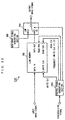
- FIG. 9 is a block diagram showing the construction of a liquid crystal device according to a first embodiment of the present invention.
- the liquid crystal display device includes a signal converting unit 401, a driving pulse generating section 902, a source driver 403, a gate driver 404, and a liquid crystal panel 405.
- the first embodiment is different from the virtual example illustrated in FIG. 4 only in the driving pulse generating section.
- the components equivalent to those illustrated in FIG. 4 are provided with the same reference numerals, and are not described herein.
- the driving pulse generating section 902 generates pulses for driving the respective drivers 403 and 404.
- the number of source lines of the liquid crystal panel 405 is ten (SL1 to SL10)
- the number of gate lines is ten (GL1 to GL10)
- one frame period is composed of ten horizontal periods.
- An input image signal is doubled in speed line by line in the signal converting section 401, and is then supplied to the source driver 403.
- the signal converting section 401 From the signal converting section 401, a non-image signal and an image signal that have been doubled in speed line by line are outputted in time sequence during one horizontal period of the input signal.
- the source driver 403 alternately inverts the signal (double-speed signal) outputted from the signal converting section 401 for supply to the source lines (SL1 to SL10) of the liquid crystal panel 405.
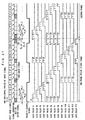
- FIG. 10 and FIG. 11 are illustrations showing, as an example of alternate inversion, timing of a polarity control signal and timing of each driver driving pulse, respectively, when line-by-line inversion and frame-by-frame inversion are combined.
- the polarity control signal for switching alternate polarity is generated by the driving pulse generating section 902 in the following manner.
- the polarity control signal is generated based on, an image period signal (A) indicating HI during image signal periods (T0_1, T0_3, T0_5 together T1_1, T1_3, ...), a frame inversion signal (B) synchronized with writing of an image signal, a frame inversion signal (C) synchronized with writing of a non-image signal, and a line-by-line inversion signal (D).
- a signal (E) obtained by XORing the signal (D) and the signal (B) and a signal (F) obtained by XORing the signal (D) and the signal (C) are generated.
- Such a signal (G) is generated as to become the signal (E) when the signal (A) is HI and become the signal (F) when the signal (A) is LOW.
- This signal (G) is a polarity control signal of a source signal.
- the frame inversion signal (B) and the frame inversion signal (C) have such a phase relation as that the signal (C) trails earlier than the signal (B), as illustrated in FIG. 10.
- the source driver 403 Based on the polarity control signal (G) generated in the above manner, the source driver 403 supplies a positive voltage when the polarity control signal (G) is HI, and supplies a negative voltage when LOW.
- the input-output characteristic of the source driver 403 has been described with reference to FIG. 8. In FIG. 11, the polarity of the voltage supplied by the source driver 403 is represented as "+" or "-" in each gate-selected period.
- gate pulses P1 through P10 are pulses for selecting ten gate lines (GL1 through GL10), respectively, on the liquid crystal panel 405 during their HI periods.
- the gate pulses P1 through P10 are driven in the following manner in accordance with timing of the double-speed signal inputted to the source driver 403.
- the gate pulse P1 becomes HI, and a negative image signal S1 is written in picture elements on the gate line GL1.
- the gate pulse P7 becomes HI, and a positive non-image signal is written in picture elements on the gate line GL7.
- the gate pulse P2 becomes HI, and a positive image signal S2 is written in picture elements on the gate line GL2.
- the gate pulse P8 becomes HI, a negative non-image signal is written in picture elements on the gate line GL8.
- G polarity control signal
- each of the gate lines (GL1 through GL10) on the liquid crystal panel 405 is selected twice during one frame period.
- an image signal and a non-image signal are written once.
- the gate pulse P1 becomes HI, and a positive image signal S'1, which is opposite in polarity of the signal in the first frame, is written in the picture elements on the game line GL1.
- the gate pulse P7 becomes HI, and a negative non-image signal, which is opposite in polarity to the signal in the first signal, is written in the picture elements on the gate line GL7, Thereafter, similarly, signals opposite in polarity to those in the first frame are sequentially written.
- a non-image signal (B) equal in polarity to the image signal is always written. Furthermore, after the non-image signal (B) is written, the image signal opposite in polarity to the non-image signal is always written. Therefore, the degree of writing of image signals in the respective picture elements is made even, thereby enabling image display more evenly.
- the basic driving scheme is so-called line inversion driving, in which the polarity of the signal is inverted line by line, but the present invention is not restricted thereto.
- line inversion driving in which the polarity of the signal is inverted line by line
- column inversion driving in which signals written in picture elements adjacent to each other on a line are opposite.
- FIG. 12 is a block diagram illustrating the construction of a liquid crystal display device according to a second embodiment of the present invention.
- the liquid crystal device includes a signal converting section 401, a driving pulse generating section 1202, a source driver 403, a gate driver 404, and a liquid crystal panel 405.
- the second embodiment is different from the first embodiment illustrated in FIG. 9 only in the driving pulse generating section.
- the components equivalent to those illustrated in FIG. 9 are provided with the same reference numerals, and are not described herein.
- the driving pulse generating section 1202 generates pulses for driving the respective drivers 403 and 404.
- the number of source lines of the liquid crystal panel 405 is ten (SL1 through SL10)
- the number of gate lines is ten (GL1 through GL10)
- one frame period is composed of ten horizontal periods.
- An input image signal is doubled in speed line by line in the signal converting section 401, and is then supplied to the source driver 403.
- the signal converting section 401 From the signal converting section 401, a non-image signal and an image signal that have been doubled in speed line by line are outputted in time sequence during one horizontal period of the input signal.
- the source driver 403 alternately inverts the signal (double-speed signal) outputted from the signal converting section 401 for supply to the source lines (SL1 through SL10) of the liquid crystal panel 405.
- FIG. 13 and FIG. 14 are illustrations showing, as one example of alternate inversion, timing of a polarity control signal and timing of each driver driving pulse, respectively, when line-by-line inversion and frame-by-frame inversion are combined.
- the polarity control signal for switching the alternate polarity is generated by the driving pulse generating section 1202 in the following manner.
- the polarity control signal is generated based on an image period signal (A) indicating HI during image signal periods (T0_1, T0_3, T0_5 together T1_1, T1_3, ...), a frame inversion signal (B) synchronized with writing of an image signal, a frame inversion signal (C) synchronized with writing of a non-image signal, and a line-by-line inversion signal (D).
- a signal (E) obtained by XORing the signal (D) and the signal (B) and a signal (F) obtained by XORing the signal (D) and the signal (C) are generated.
- Such a signal (G) is generated as to become the signal (E) when the signal (A) is HI and become the signal (F) when the signal (A) is LOW.
- This signal (G) is a polarity control signal of a source signal.
- the frame inversion signal (B) and the frame inversion signal (C) have such a phase relation as that the signal (C) trails earlier than the signal (B), as illustrated in FIG. 13.
- the source driver 403 Based on the polarity control signal (G) generated in the above manner, the source driver 403 supplies a positive voltage when the polarity control signal (G) is HI, and supplies a negative voltage when LOW.
- the input-output characteristic of the source driver 403 has been described with reference to FIG. 8.
- the polarity of the voltage supplied by the source driver 403 is represented as "+" or "-" in each gate-selected period.
- gate pulses P1 through P10 are pulses for selecting ten gate lines (GL1 through GL10) respectively, on the liquid crystal panel 405 during their HI periods.
- the gate pulses P1 through P10 are driven in the following manner in accordance with timing of the double-speed signal inputted to the source driver 403.
- the gate pulse P1 becomes HI, and a negative image signal S1 is written in picture elements on the gate line GL1.
- the gate pulse P7 becomes HI, and a negative non-image signal is written in picture elements on the gate line GL7.
- the gate pulse P2 becomes HI, and a positive image signal S2 is written in picture elements on the gate line GL2.
- the gate pulse P8 becomes HI, a negative non-image signal is written in picture elements on the gate line GL8.
- G polarity control signal
- each of the gate lines (GL1 through GL10) on the liquid crystal panel 405 is selected twice during the one frame period.
- an image signal and a non-image signal are written once.
- the gate pulse P1 becomes HI, and a positive image signal S'1, which is opposite in polarity of the signal in the first frame, is written in the picture elements on the game line GL1.
- the gate pulse P7 becomes HI, and a positive non-image signal, which is opposite in polarity to the signal in the first signal, is written in the picture elements on the gate line GL7, Thereafter, similarly, signals opposite in polarity to those in the first frame are sequentially written.
- a non-image signal (B) opposite in polarity to the image signal is always written. Furthermore, after the non-image signal (B) is written, the image signal equal in polarity to the non-image signal is always written. Therefore, the degree of writing of image signals in the respective picture elements is made even, thereby enabling image display more evenly.
- the basic driving scheme is so-called line inversion driving, in which the polarity of the signal is inverted line by line, but the present invention is not restricted thereto.
- line inversion driving in which the polarity of the signal is inverted line by line
- column inversion driving in which signals written in picture elements adjacent to each other on a line are opposite.
- the driving frequency is double that of normal driving and, as a result, the time allocated for writing an image signal in each picture element is reduced by 1/2. Therefore, with upsizing and high-resolution of the liquid crystal panel, writing an image signal in each picture element may not be sufficiently carried out, in some cases.
- pre-charge driving is introduced to the driving scheme of the first embodiment, where, immediately prior to writing an original image signal in a picture element, a non-image signal equal in polarity thereto is written.
- FIG. 15 is a block diagram illustrating the construction of a liquid crystal device according to the third embodiment of the present invention.
- the liquid crystal device includes a signal converting section 401, a driving pulse generating section 1502, a source driver 403, a gate driver 404, a liquid crystal panel 405.
- the third embodiment is different from the first embodiment illustrated in FIG. 9 only in the driving pulse generating section.
- the components equivalent to those illustrated in FIG. 9 are provided with the same reference numerals, and are not described herein.
- the driving pulse generating section 1502 generates pulses for driving the respective drivers 403 and 404.
- the number of source lines of the liquid crystal panel 405 is ten (SL1 to SL10)
- the number of gate lines is eleven (GL1 to GL11)
- one frame period is composed of eleven horizontal periods.
- An input image signal is doubled in speed line by line in the signal converting section 401, and is then supplied to the source driver 403.
- the signal converting section 401 From the signal converting section 401, a non-image signal and an image signal that have been doubled in speed by line are outputted in time sequence during one horizontal period of the input signal.
- the source driver 403 alternately inverts the signal (double-speed signal) outputted from the signal converting section 401 for supply to the source lines (SL1 to SL10) of the liquid crystal panel 405.
- FIG. 16 is an illustration showing, as an example of alternate inversion, timing of a polarity control signal and driver driving pulses when line-by-line inversion and frame-by-frame inversion are combined.
- the polarity control signal for switching the alternate polarity is generated by the driving pulse generating section 1502 in a manner equivalent to that in the first embodiment.
- the source driver 403 Based on the polarity control signal, the source driver 403 supplies a positive voltage when the polarity control signal is HI, and supplies a negative voltage when LOW.
- the input-output characteristic of the source driver 403 has been described with reference to FIG. 8.
- the polarity of the voltage supplied by the source driver 403 is represented as "+" or "-" in each gate-selected period.
- gate pulses P1 through P11 are pulses for selecting eleven gate lines (GL1 through GL11), respectively, on the liquid crystal panel 405 during their HI periods.
- the gate pulses P1 through P11 are driven in the following manner in accordance with timing of the double-speed signal inputted to the source driver 403.
- the gate pulse P1 becomes HI, and a positive image signal S1 is written in picture elements on the gate line GL1.
- the gate pulses P2 and P5 become HI, and negative non-image signals are written in picture elements on the gate lines GL2 and GL5, respectively.
- the gate pulse P2 becomes HI, and a negative image signal S2 is written in the picture elements on the gate line GL2.
- the gate pulses P3 and P6 become HI, and positive non-image signals are written in picture elements on the gate lines GL3 and GL6. Thereafter, signals are sequentially written as illustrated in FIG. 16.
- each of the gate lines (GL1 through GL11) on the liquid crystal panel 405 is selected three times during one frame period. In the picture elements on each gate line, one image signal and two non-image signals are written.
- the gate pulse P1 becomes HI, and a negative image signal S'1, which is opposite in polarity of the signal in the first frame, is written in picture elements on the game line GL1.
- the gate pulses P2 and P5 become HI, and negative non-image signals, which are opposite in polarity to those in the first signal, are written in the picture elements on the gate lines GL2 and GL5, respectively. Thereafter, similarly, signals opposite in polarity to those in the first frame are sequentially written.
- a non-image signal equal in polarity to the image signal is preliminarily written, thereby making it possible to sufficiently charge the picture elements. Therefore, the problem of insufficient charge caused by a short writing time can be resolved, and more desirable display image quality can be obtained.
- the device is so constructed as that the non-image signal is written 7.5 horizontal periods after the time when the image signal is written. Therefore, a non-image signal to be written for pre-charge prior to writing of the image signal (hereinafter referred to as pre-charge signal) is written 0.5 horizontal period before the time when the image signal is written.
- pre-charge signal a non-image signal to be written for pre-charge prior to writing of the image signal
- the pre-charge signal can be written 1.5 horizontal periods before the image signal.
- the phase of the pre-charge signal is determined based on the relation in phase between the image signal and the non-image signal.
- one frame period be an odd multiple of one horizontal period. Therefore, it is more desirable that a rate changing section using a memory or the like be provided for changing a signal rate as appropriate so that one frame period is always an odd multiple of one horizontal period.
- the basic driving scheme is so-called line inversion driving, in which the polarity of the signal is inverted line by line, but the present invention is not restricted thereto.
- line inversion driving in which the polarity of the signal is inverted line by line
- column inversion driving in which signals written in picture elements adjacent to each other on a line are opposite, may be used to obtain.
- the driving frequency is double that of normal driving and, as a result, the time allocated for writing a non-image signal in each picture element is reduced to 1/2. Therefore, with upsizing and high-resolution of the liquid crystal panel, writing a non-image signal in each picture element may not be sufficiently carried out, in some cases.
- a fourth embodiment of the present invention to solve the above problem, so-called dual-charge driving is introduced to the driving scheme of the second embodiment, where, immediately after writing a non-image signal in a picture element, a non-image signal equal in polarity thereto is written.
- FIG. 18 is a block diagram illustrating the construction of a liquid crystal device according to the fourth embodiment of the present invention.
- the liquid crystal device includes a signal converting section 401, a driving pulse generating section 1802, a source driver 403, a gate driver 404, a liquid crystal panel 405.
- the fourth embodiment is different from the second embodiment illustrated in FIG. 12 only in the driving pulse generating section.
- the components equivalent to those illustrated in FIG. 12 are provided with the same reference numerals, and are not described herein.
- the driving pulse generating section 1802 generates pulses for driving the respective drivers 403 and 404.
- the number of source lines of the liquid crystal panel 405 is ten (SL1 to SL10)
- the number of gate lines is eleven (GL1 to GL11)
- one frame period is composed of eleven horizontal periods.
- An input image signal is doubled in speed line by line in the signal converting section 401, and is then supplied to the source driver 403.
- the source driver 403 alternately inverts the signal (double-speed signal) outputted from the signal converting section 401 for supply to the source lines (SL1 to SL10) of the liquid crystal panel 405.
- FIG. 19 is an illustration showing, as an example of alternate inversion, timing of a polarity control signal and driver driving pulses when line-by-line inversion and frame-by-frame inversion are combined.
- the polarity control signal for switching the alternate polarity is generated by the driving pulse generating section 1802 in a manner equivalent to that in the second embodiment.
- the source driver 403 Based on the polarity control signal, the source driver 403 supplies a positive voltage when the polarity control signal is HI, and supplies a negative voltage when LOW.
- the input-output characteristic of the source driver 403 has been described with reference to FIG. 8.
- the polarity of the voltage supplied by the source driver 403 is represented as "+" or "-" in each gate-selected period.
- gate pulses P1 through P11 are pulses for selecting eleven gate lines (GL1 through GL11) , respectively, on the liquid crystal panel 405 during their HI periods.
- the gate pulses P1 through P11 are driven in accordance with timing of the double-speed signal inputted to the source driver 403 in the following manner.
- the gate pulse P1 becomes HI, and a positive image signal S1 is written in picture elements on the gate line GL1.
- the gate pulses P5 and P7 become HI, and positive non-image signals are written in picture elements on the gate lines GL7 and GL5.
- the gate pulse P2 becomes HI, and a negative image signal S2 is written in picture elements on the gate line GL2.
- the gate pulses P6 and P8 become HI, and negative non-image signals are written in picture elements on the gate lines GL3 and GL6. Thereafter, signals are sequentially written as illustrated in FIG. 19.
- each of the gate lines (GL1 through GL11) on the liquid crystal panel 405 is selected three times during one frame period. In the picture elements on each gate, one image signal and two non-image signals are written.
- the gate pulse P1 becomes HI, and a negative image signal S'1, which is opposite in polarity of the signal in the first frame, is written in the picture elements on the game line GL1.
- the gate pulses P5 and P7 become HI, and negative non-image signals, which are opposite in polarity to those in the first frame, are written in the picture elements on the gate lines GL5 and GL7, respectively. Thereafter, similarly, signals opposite in polarity to those in the first frame are sequentially written.
- the fourth embodiment after writing of a non-image signal, another non-image signal equal in polarity to the non-image signal is posteriorly written, thereby making it possible to sufficiently charge the picture elements. Therefore, the problem of insufficient charge caused by a short writing time can be improved, and more desirable display image quality can be obtained.
- FIG. 19 described is a case where, after writing of a non-image signal, another non-image signal equal in polarity to the non-image signal is posteriorly written.
- an image signal equal in polarity to the non-image signal may be used for pre-charging.
- one frame period be an odd multiple of one horizontal period. Therefore, it is more desirable that a rate changing section using a memory or the like be provided for changing a signal rate as appropriate so that one frame period is always an odd multiple of one horizontal period.
- the basic driving scheme is so-called line inversion driving, in which the polarity of the signal is inverted line by line, but the present invention is not restricted thereto.
- line inversion driving in which the polarity of the signal is inverted line by line
- column inversion driving in which signals written in picture elements adjacent to each other on a line are opposite.
- FIG. 21 is a block diagram illustrating the construction of a liquid crystal display device according to a fifth embodiment of the present invention.
- the liquid crystal device includes a signal converting section 2101, a driving pulse generating section 2102, a source driver 403, a gate driver 404, and a liquid crystal panel 405.
- the fifth embodiment is different from the first embodiment illustrated in FIG. 9 only in the driving pulse generating section and the signal converting section.
- the components equivalent to those illustrated in FIG. 9 are provided with the same reference numerals, and are not described herein.
- the signal converting section 2101 converts an input image signal in a manner that will be described later.
- the driving pulse generating section 2102 generates pulses for driving the respective drivers 403 and 404.
- the number of source lines of the liquid crystal panel 405 is ten (SL1 through SL10)
- the number of gate lines is twelve (GL1 through GL12)
- one frame period is composed of twelve horizontal periods.
- written in each picture element on the liquid crystal panel 405 are an image signal and a non-image signal irrespective of this image signal for suppressing a back transition phenomenon of the OCB liquid crystal, and these signals are written once every frame period.
- the signal converting section 2101 converts the driving frequency.
- 1.25-times frequency conversion is shown where transfer is made for five lines (including one line of a non-image signal) to the source driver 403 during four horizontal periods of the input image signal.
- this 1.25-times frequency conversion is shown where transfer is made for five lines (including one line of a non-image signal) to the source driver 403 during four horizontal periods of the input image signal.
- FIG. 22 illustrates a specific construction of the signal converting section 2101.
- FIG. 23 illustrates timing of the converting operation.
- the control signal generating section 2201 generates various control signals, such as a clock,from a synchronizing signal synchronized with the input image signal.
- the input image signal is written in the line memory 502 in synchronization with a write clock from the control generating section 2201.
- the image signal written in the line memory 502 is read from the line memory 502 in synchronization with a read clock (having a frequency 1.25 times higher than that of the write clock) from the control signal generating section 2201, and this reading is carried out during a period four-fifth of that of writing.
- a read clock having a frequency 1.25 times higher than that of the write clock
- the output signal selecting section 504 selects this image signal as an output and, during the remaining period, selects a non-image signal outputted from a non-image signal generating section 503 as an output. Consequently, from the signal converting section 2101, as illustrated in FIG. 23, a non-image signal and a image signal both made 1.25 times faster in speed are outputted in time sequence at the ratio of 1:4.
- the input/output characteristic of the source driver 403 has been described with reference to FIG. 8.
- the source driver 403 inverts the polarity of the signal outputted from the signal converting section 2101 by several lines for output.
- FIG. 24 is an illustration showing timing of the signal outputted from the signal converting section 2101, a polarity control signal, and gate driver driving pulses.
- the polarity of a voltage supplied by the source driver 403 is represented as "+” or "-" in each gate-selected period. This polarity is switched based on the polarity control signal generated in the driving pulse generating section 2102.
- gate pulses P1 through P12 are pulses for selecting ten gate lines (GL1 through GL12), respectively, on the liquid crystal panel 405 during their HI periods.
- the gate pulses P1 through P12 are driven in the following manner in accordance with timing of the signal outputted from the signal converting section 2101 to the source driver 403.
- the gate pulses P5 through P8 simultaneously become HI, and positive non-image signals are written in picture elements on the gate lines GL5 through GL8.
- the gate pulses P1 through P4 sequentially become HI, and positive image signals S1 through S4 are sequentially written on the gate line GL1 through GL4.
- the gate pulses P9 through P12 simultaneously become HI, and negative non-image signals are written on the gate lines GL9 through GL12.
- the gate pulses P5 through P8 sequentially become HI, and negative image signals S5 through S8 are sequentially written on the gate lines GL5 through GL8.
- the picture elements on the gate lines GL5 through GL8 retain the non-image signal during the periods T0_0 through T0_5, the periods T0_0 through T0_6, the periods T0_0 through T0_7, the periods T0_0 through T0_8, respectively.
- each of the gate lines (GL1 through GL12) on the liquid crystal panel 405 is selected twice during one frame period.
- an image signal and a non-image signal is written once.
- the gate pulses P5 through P8 simultaneously become HI, and negative non-image signals, which are opposite in polarity of those in the first frame, are written on the gate lines GL5 through GL8.
- the gate pulses P1 through P4 sequentially become HI, and negative image signals S'1 through S'4, which are opposite in polarity of those in the first frame, are sequentially written on the gate lines GL1 through GL4.
- non-image signals are simultaneously written in a plurality of gate lines. Therefore, as illustrated in FIG. 23, a period allocated for recharging the picture elements becomes longer than that in the above-described virtual example and the first to fourth embodiments. Consequently, it is possible to solve the problem of insufficient recharging caused by writing of the non-image signal, thereby suppressing image deterioration. It is also possible to prevent the transfer rate to the source driver 403 from becoming high-speed, thereby reducing loads on circuits. Note that, as far as solving the problems of insufficient recharging and circuit loads is concerted, consideration is not necessarily given to a balance in polarity changes.
- the basic driving scheme is so-called line inversion driving, in which the polarity of the signal is inverted by several lines, but the present invention is not restricted thereto.
- line inversion driving in which the polarity of the signal is inverted by several lines
- column inversion driving in which signals written in picture elements adjacent to each other on a line are opposite in polarity.
- the length of time from the time when a non-image signal is written on picture elements on a gate line to the time when an image signal is written next is the one as illustrated in FIG. 24 (for example, the length of the periods T0_11 through T1_1 for the gate line GL1).
- the present invention is not restricted thereto.
- the period for inserting a non-image signal should be changed into an optimum one as appropriate according to system changes, such as material for the liquid crystal is replaced. Also, it is clear that the period for inserting a non-image signal will affect the brightness, and therefore this inserting period may be arbitrarily changed by the user.
- the driving frequency is 1.25 times higher than that at normal driving and, consequently, a time allocated for writing an image signal in each picture element is shortened by 1/1.25. Therefore, with upsizing and high-resolution of the liquid crystal panel, writing an image signal in each picture element may not be sufficiently carried out, in some cases.
- pre-charge driving is introduced to the driving scheme of the fifth embodiment, where, immediately prior to writing an original image signal in each picture element, an image signal equal in polarity thereto is written.
- FIG. 25 is a block diagram illustrating the construction of a liquid crystal device according to the sixth embodiment of the present invention.
- the liquid crystal device includes a signal converting section 2101, a driving pulse generating section 2502, a source driver 403, a gate driver 404, a liquid crystal panel 405.
- the sixth embodiment is different from the fifth embodiment illustrated in FIG. 21 only in the driving pulse generating section.
- the components equivalent to those illustrated in FIG. 21 are provided with the same reference numerals, and are not described herein.
- the driving pulse generating section 2502 generates pulses for driving the respective drivers 403 and 404.
- the signal converting section 2101 converts the driving frequency. That is, transfer is made for five lines (including one line of a non-image signal) to the source driver 403 during four horizontal periods of the input image signal.
- the source driver 403 inverts the polarity of the signal outputted from the signal converting section 2101 by several lines for output.
- FIG. 26 is an illustration showing timing of the input image signal, the output signal outputted from the signal converting section 2101, a polarity control signal, and gate driver driving pulses.
- gate pulses P1 and P5 through P8 simultaneously become HI, and positive non-image signals are written in picture elements on gate lines GL1 and GL5 through GL8.
- the gate pulse P1 continues to be HI and, simultaneously, a gate pulse P2 becomes HI, and positive image signals S1 are written in picture elements on gate lines GL1 and GL2.
- the picture elements on the gate line GL1 have the positive non-image signal written therein immediately before, and therefore writing of the positive image signal S1 becomes easy.
- gate pulses P2 and P3 simultaneously become HI.
- gate pulses P5 and P9 through P12 simultaneously become HI, and negative non-image signals are written in picture elements on gate lines GL5 and GL9 through GL12.
- the gate pulse P5 continues to be HI, further a gate pulse P6 simultaneously becomes HI, and negative image signals S5 are written in picture elements on gate lines GL5 and GL6.
- the picture elements on the gate line GL5 have the negative non-image signal already written therein. Therefore, writing of also the negative image signal S5 becomes easy.
- Each picture element on the gate line GL5 retains the non-image signal during the periods T0_0 through T0_5, and retains the image signal during the remaining period in the first frame.
- a second frame During a first period T1_0 in the second frame, the gate pulses P1 and P5 through P8 simultaneously become HI, and negative non-image signals, which are opposite in polarity to those in the first frame, are written in the picture elements on the gate lines GL1, GL5 through GL8.
- the gate pulse P1 continues to be HI and, further the gate pulse P2 becomes HI, negative image signals S'1, which are opposite in polarity to those in the first frame, are written in the picture elements on the gate lines GL1 and GL2.
- the basic driving scheme is so-called line inversion driving, in which the polarity of the signal is inverted line by line, but the present invention is not restricted thereto.
- line inversion driving in which the polarity of the signal is inverted line by line
- column inversion driving in which signals written in picture elements adjacent to each other on a line are opposite.
- pre-charging is applied to the driving scheme for carrying out (n + 1)/(n)-times speed conversion.
- Dual-charge driving as shown in the fourth embodiment can be applied to the scheme for carrying out (n + 1)/(n)-times speed conversion.
- the polarity of non-image signals simultaneously written on a plurality of gate lines are opposed to the polarity of the image signals previously written, writing of the non-image signals become disadvantageous.
- other non-image signals equal in polarity to the non-image signals (that is, opposite in polarity to the image signals written prior to these non-image signals) are auxiliarily written again (dual-charge), thereby reliably writing the non-image signals.
- timing of writing again non-image signals equal in polarity of the already-written non-image signals is, for example, after ten scanning periods in a case of the driving scheme for carrying out 1.25-times speed conversion (relative positional relation such as the period T0_10 with respect to the period T0_0).
- the number of lines during one frame period is subjected to restrictions.
- the total number of lines Y during one frame period should be N ⁇ (2M + 1) (M is an integer not less than 1).
- periods during which picture elements on gate lines GL1 through GL4 retain an image signal are periods T0_1 through T0_9, periods T0_2 through T0_9, periods T0_3 through T0_9, and periods T0_4 through T0_9, respectively.
- periods during which each picture element on a gate line GL5 retains an image signal are periods T0_6 through T0_14. That is, the periods during which each picture element on the gate line GL5 retains the image signal become equal in length to the periods during which each picture element on the gate line GL1 retains the image signal.
- the periods during which each picture element on the gate lines GL6 through GL8 retains the image signal become equal in length to the periods during which each picture element on the gate lines GL2 through GL4 retains the image signal.
- periods during which each picture element on the gate lines GL9 through GL12 retains the image signal are periods T0_11 through T1_4, periods T0_12 through T1_4, periods T0_13 through T1_4, and periods T0_14 through T1_4, respectively, and each include a period T0_16. Therefore, those periods differ in length from the periods during which each picture element on the other gate lines retains the image signal. As a result, a difference in brightness occurs between a display portion corresponding to the gate lines GL1 through GL8 and a display portion corresponding to the gate lines GL9 through GL12.
- a means for adjusting the number of gate lines to be scanned for one frame period is newly provided, thereby adjusting the total number of scanning lines Y for one frame period of the input image signal to N ⁇ (2M + 1), when Y is not N ⁇ (2M + 1).
- FIG. 28 is a block diagram illustrating a liquid crystal display device according to a seventh embodiment of the present invention.
- the liquid crystal display device includes a signal converting section 2101, a drive pulse generating section 2802, a source driver 403, a gate driver 404, a liquid crystal panel 405, a number-of-lines adjusting section 2806, and a frame memory 2807.
- the seventh embodiment is different from the sixth embodiment illustrated in FIG. 25 only in that the number-of-lines adjusting section 2806 and the frame memory 2807 are newly provided.
- the components equivalent to those illustrated in FIG. 25 are provided with the same reference numerals, and are not described herein.
- a driving scheme of the liquid crystal display device In synchronization with reference timing of a predetermined image signal, writing and reading of the image signal to and from the frame memory 2807 is carried out. At this time, the frequency of a clock used for reading the image signal from the frame memory 2807 is made lower than the frequency of a clock used for writing the image signal in the frame memory 2807.
- the number of image signals during one horizontal period maintained With the number of image signals during one horizontal period maintained, the horizontal period becomes longer, and also with one frame period maintained, the number of lines during one frame period can be reduced.
- the number of lines Y during one frame period of the input image signal is not N ⁇ (2M + 1), this number can be adjusted to N ⁇ (2M + 1). Consequently, dispersion of the periods for retaining the image signal can be suppressed, thereby enabling high-quality display.
- the number-of-lines converting section 2806 carries out conversion so that the number of lines is reduced from Y to Y' ( ⁇ Y). This is because, in general, an image signal includes a blanking period not related to an image to be displayed and, even if the total number of lines during one frame period is reduced, any part of video to be displayed will not be dropped. Furthermore, it is more advantageous to reduce the number of lines than to increase the number of lines because the operation frequency is reduced. However, when the total number of lines Y is not more than the number of lines of the image signals to be displayed, such adjustment as to satisfy Y' > Y may be carried out. This adjustment is made possible by making the frequency of the clock used for reading the image signal from the frame memory 2807 higher than the frequency of the clock used for writing the image signal in the frame memory 2807.
- the length of the periods for retaining the non-image signal during one frame period is varied by line.
- the larger the number of lines on which the non-image signals are simultaneously written the larger the variation. Consequently, luminance variations can be disadvantageously perceived on a display screen.
- luminance variations by a unit of six lines as illustrated in FIG. 30 can be disadvantageously perceived.
- these luminance variations are resolved by correcting the luminance of the input image signal.
- FIG. 31 is a block diagram illustrating the construction of a liquid crystal display device according to the eighth embodiment.
- the liquid crystal display device includes a luminance correcting section 3108, a signal converting section 3101, a driving pulse generating section 3102, a source driver 403, a gate driver 404, and a liquid crystal panel 405.
- the signal converting section 3101 includes a line memory 502.
- the components equivalent to those illustrated in FIG. 21 or FIG. 22 are provided with the same reference numerals, and are not described herein.
- the signal converting section 3101 and the driving pulse generating section 3102 respectively carry out predetermined signal processing so as to achieve a driving scheme illustrated in FIG. 29.
- This signal processing is evident from the above description of the embodiments, and therefore not described herein.
- the luminance correcting section 3108 corrects the luminance of the input image signal at a predetermined degree previously obtained through an experiment, etc., so that luminance variations as illustrated in FIG. 30 are eliminated.
- a scheme for correction various schemes can be used, such as a scheme using a table, or a scheme for using a multiplier.
- FIG. 32 is a block diagram illustrating the construction of a liquid crystal display device according to a ninth embodiment of the present invention.
- the liquid crystal display device includes a signal converting section 3201, a driving pulse generating section 3202, a source driver 403, a gate driver 404, and a liquid crystal panel 405.
- the signal converting section 3201 includes a memory 3209.
- the components equivalent to those illustrated in FIG. 21 are provided with the same reference numerals, and are not described herein.
- the signal converting section 3201 converts the input image signal so that the driving frequency is multiplied by 7/6 and, at the same time, rearranges the writing order by line. For these conversion and rearrangement, the memory 3209 is used.
- luminance variations are solved by correcting the image signal.
- luminance variations are solved by rearranging the scanning order by frame.
- FIG. 33A is an illustration showing timing of each of gate driver driving pulses in a first frame.
- FIG. 33B is, on the other hand, an illustration showing timing of each of gate driver driving pulses in a second frame.
- scanning is carried out in a direction from a gate line GL6 to a gate line GL1, and then in a direction from a gate line GL7 to a gate line GL12.
- scanning is carried out in a direction from the gate line GL1 to the gate line GL6, and then in a direction from the gate line GL12 to the gate line GL7.
- scanning illustrated in FIG. 33A and scanning illustrated in FIG. 33B are alternately carried out by one frame.
- the signal converting section 3201 rearranges the image signals and converts the driving frequency.
- the construction for carrying out such signal processing has been known to public, and therefore is not described herein.
- the average periods during which the non-image signal is inserted can be equalized in each gate by changing the scanning direction for each frame. Therefore, it is possible to prevent luminance variations from being perceived.
- a predetermined voltage for preventing back transition is applied as a non-image signal to a liquid crystal through a source line.
- a predetermined voltage is applied to the liquid crystal by controlling the potential at the electrode 3401 of a picture element section illustrated in FIG. 34.
- the picture element section of the liquid crystal panel has, in general, a liquid crystal 202 held between a picture element electrode and a common electrode 201, and a storage capacitor 203 formed between the picture element electrode and the electrode 3401. Note that, in FIG. 34, the components equivalent in structure to those in FIG. 2 are provided with the same reference numerals, and are not described herein.
- the electrode 3401 is connected to the common electrode 201 as illustrated in FIG. 2. In the following embodiments, however, the electrode 3401 is an independent electrode from the common electrode 201. In the following description, for convenience sake, the electrode 3401 is referred to as "the other-end electrode”. That is, of the electrodes of the storage capacitor 203 at both ends, the one located on a side that is not connected to a drain line is called “the other-end electrode”.
- FIG. 35 is a block diagram illustrating the construction of the liquid crystal display device according to the tenth embodiment.
- the liquid crystal display device includes a signal processing section 3601, a driving pulse generating section 3602, a gate driver 101, a source driver 102, a liquid crystal panel 3605, and the other-end driver 3501.
- the components equivalent in structure to those in FIG. 1 or FIG. 2 are provided with the same reference numerals, and are not described herein.
- the signal processing section 3601 carries out normal signal processing associated with image processing, and is the same as a conventional one.
- the driving pulse generating section 3602 generates a control signal to be supplied to each driver, and is the same as a conventional one, except for generating a control signal for the other-end driver. That is, processing in the gate driver 101 and the source driver 102 is similar to the conventional one.
- the liquid crystal display device of the tenth embodiment is different from the conventional one in that a potential for preventing back transition is applied to the liquid crystal panel 3605 through the other-end driver 3501.
- FIG. 37 Hereinafter described is the operation of the present embodiment with reference to FIG. 37.
- a potential Vg of each of gate lines (GL1, GL2, ...) sequentially becomes ON for each frame in synchronization with a data potential Vs supplied to a source line (SL1, SL2, ).
- the polarity of the voltage supplied to the source line is switched by each source line and each frame.
- a difference between the potential given to the picture element electrode through the source line in the above described manner and the potential of the common electrode 201 is a voltage to be applied to the liquid crystal 202 in the picture element 104.
- the voltage applied to the liquid crystal 202 determines a transmittance of this picture element 104.
- the potential of the other-end electrode 3401 influences the voltage applied to the liquid crystal 202 through the storage capacitor 203. Therefore, as exemplarily illustrated in FIG. 37, by changing a potential Ve of the other-end electrode 3401, the potential difference between both ends of the liquid crystal 202 can be manipulated.
- Vp the amount of change in voltage applied to the liquid crystal 202 (cumulative potential) Vp is represented as the following equation (1), where the storage capacitor is Cst, a liquid crystal capacitance is Clc, a parasitic capacitance between the gate and the drain not shown is Cgd, and a voltage change in Ve is Ve+ or Ve-.
- Vp Cst / (Clc + Cst + Cgd) ⁇ (Ve+ or Ve-)
- a voltage required for preventing back transition can be applied to the liquid crystal 202 as appropriate. That is, irrespectively of the potential given to the liquid crystal through the source line, effective voltages can be arbitrarily (the above-described Vp) accumulated. Therefore, without shortening the time for writing the image signal, the predetermined voltage for preventing back transition can be regularly (for example, 20% of one frame period for each frame) applied to the liquid crystal 202.
- the predetermined voltage can be applied to the liquid crystal 202 without influencing writing of the image signal. This does not pose such problems as image deterioration due to insufficient recharge of the image signal or load increase on circuits due to high speed of the driving frequency.
- alternate inversion of the voltage to be applied to the liquid crystal 202 is achieved by inverting the polarity of the source-line potential.
- the source line has to be supplied with a potential at least double in width of the potential (black potential) 305 when the transmittance is at the lowest as illustrated in FIG. 3.
- alternate inversion driving and anti-back transition preventing driving are simultaneously achieved while the source line is supplied with a potential one-fold in width of the potential 305 (hereinafter referred to as one-fold potential) illustrated in FIG. 3.
- FIG. 38 is a block diagram illustrating a liquid crystal display device according to an eleventh aspect of the present invention.
- the liquid crystal display device includes a signal processing section 3801, a driving pulse generating section 3802, a gate driver 101, a source driver 102, the other-end driver 3501, and a liquid crystal panel 3605.
- the components equivalent in structure to those in FIG. 36 are provided with the same reference numerals, and are not described herein.
- Described first is a mechanism for achieving alternate inversion driving while supplying a one-fold potential to the source line.
- Vcc Cst / (Clc + Cst +Cgd) ⁇ (Vge+ or Vge-)
- part to be written as negative in the end is subjected to processing, such as bit inversion, by the signal processing section 3801, for example, so that the luminance when the signal is written as negative coincides with the original luminance.
- the potential in the other-end electrode 3401 is further changed after 80% of the period of one frame has passed, for example, and then the potential of the other-end electrode 3401 is further changed (Ve+ or Ve-) and kept in that state. With this, the voltage required for preventing back transition can be applied to the liquid crystal 202 through the storage capacitor 203.
- the amount of change Vp in potential applied to the liquid crystal can be represented as the above equation (1), where the amount of change in Ve is Ve+ or Ve-.
- the eleventh embodiment in addition to the effects of the tenth embodiment, it is possible to carry out alternate inversion driving while driving the source line by a one-fold potential. Therefore, it is possible to reduce cost of a circuit for driving the source line or cost of a driver IC.
- the other-end electrode 3401 is driven by the other-end driver 3401.
- driving has some disadvantages, such as requiring a new driver, or providing a new wiring to the liquid crystal panel 3605, resulting in reduction in aperture ratio.
- the other-end electrode 3401 is connected to a gate line of an adjacent picture element (hereinafter referred to as preceding-step gate) for supplying a potential to the other-end electrode 3401 for preventing back transition, thereby preventing the above disadvantages.
- FIG. 40 is a block diagram illustrating the construction of a liquid crystal display device according to a twelfth embodiment of the present invention.
- the liquid crystal display device includes a signal processing section 3601, a driving pulse generating section 4002, a gate driver 101, a source driver 102, and a liquid crystal panel 4005.
- the components equivalent to those in FIG. 36 are provided with the same reference numerals, and are not described herein.
- FIG. 41 illustrates the detailed construction of the liquid crystal panel 4005.
- the other-end electrode 3401 is connected to a preceding-step gate 4102, which is an adjacent gate line.
- the potential of the preceding-step gate Vg(n - 1) is changed (Ve+ or Ve-) and kept in that state. With this, the voltage required for preventing back transition can be applied to the liquid crystal 202 through the storage capacitor 203.
- the other-end electrode 3401 is connected to the preceding-step gate, and the potential given to this preceding-step gate is manipulated for preventing a back transition phenomenon.
- the liquid crystal panel 3605 does not have to be provided with a new wiring, and therefore the problem of reduction in aperture ratio does not occur. Also, no new driver is required.
- the liquid crystal display device achieves improvements in evenness in image display or solves insufficiency in recharge at the time of periodically writing a non-image signal in addition to an image signal, thereby enabling image display with higher image quality.
Landscapes
- Physics & Mathematics (AREA)
- Engineering & Computer Science (AREA)
- General Physics & Mathematics (AREA)
- Crystallography & Structural Chemistry (AREA)
- Chemical & Material Sciences (AREA)
- Theoretical Computer Science (AREA)
- Computer Hardware Design (AREA)
- Nonlinear Science (AREA)
- Mathematical Physics (AREA)
- Optics & Photonics (AREA)
- Liquid Crystal (AREA)
- Liquid Crystal Display Device Control (AREA)
- Control Of Indicators Other Than Cathode Ray Tubes (AREA)
- Transforming Electric Information Into Light Information (AREA)
Applications Claiming Priority (5)
| Application Number | Priority Date | Filing Date | Title |
|---|---|---|---|
| JP2001027881A JP2002229004A (ja) | 2001-02-05 | 2001-02-05 | 液晶表示装置 |
| JP2001027881 | 2001-02-05 | ||
| JP2001131414A JP3534086B2 (ja) | 2001-04-27 | 2001-04-27 | 液晶表示装置の駆動方法 |
| JP2001131414 | 2001-04-27 | ||
| PCT/JP2002/000824 WO2002063384A1 (fr) | 2001-02-05 | 2002-02-01 | Unite d"affichage a cristaux liquides et procede d"attaque de ce dernier |
Publications (2)
| Publication Number | Publication Date |
|---|---|
| EP1286202A1 true EP1286202A1 (fr) | 2003-02-26 |
| EP1286202A4 EP1286202A4 (fr) | 2007-06-06 |
Family
ID=26608899
Family Applications (1)
| Application Number | Title | Priority Date | Filing Date |
|---|---|---|---|
| EP02710455A Withdrawn EP1286202A4 (fr) | 2001-02-05 | 2002-02-01 | Unite d'affichage a cristaux liquides et procede d'attaque de ce dernier |
Country Status (7)
| Country | Link |
|---|---|
| US (2) | US6989812B2 (fr) |
| EP (1) | EP1286202A4 (fr) |
| KR (2) | KR100748840B1 (fr) |
| CN (2) | CN100433119C (fr) |
| CA (1) | CA2404787C (fr) |
| TW (1) | TW538408B (fr) |
| WO (1) | WO2002063384A1 (fr) |
Cited By (15)
| Publication number | Priority date | Publication date | Assignee | Title |
|---|---|---|---|---|
| EP1256927A3 (fr) * | 2001-05-11 | 2004-05-06 | Thomson Licensing S.A. | Insertion de lignes noires dans des images affichées sur des grands dispostifs d'affichage à cristaux liquides |
| WO2004109642A1 (fr) * | 2003-06-04 | 2004-12-16 | Koninklijke Philips Electronics N.V. | Afficheur electrophoretique |
| KR100652096B1 (ko) | 2004-08-13 | 2006-12-01 | 도시바 마쯔시따 디스플레이 테크놀로지 컴퍼니, 리미티드 | 게이트선 구동 회로 |
| KR100701135B1 (ko) | 2004-08-06 | 2007-03-29 | 도시바 마쯔시따 디스플레이 테크놀로지 컴퍼니, 리미티드 | 게이트선 구동 회로 |
| EP1429311A3 (fr) * | 2002-11-21 | 2007-12-26 | Pioneer Corporation | Appareil de commande d'affichage, système d'affichage et méthode de commande d'affichage |
| WO2008152847A1 (fr) | 2007-06-12 | 2008-12-18 | Sharp Kabushiki Kaisha | Dispositif d'affichage à cristaux liquides, procédé de commande de dispositif d'affichage à cristaux liquides et récepteur de télévision |
| EP2071553A4 (fr) * | 2006-09-28 | 2010-10-27 | Sharp Kk | Appareil d'affichage à cristaux liquides, circuit de commande, procédé d'entraînement et récepteur de télévision |
| US8115716B2 (en) | 2005-08-04 | 2012-02-14 | Sharp Kabushiki Kaisha | Liquid crystal display device and its drive method |
| EP2369573A4 (fr) * | 2008-11-26 | 2012-05-09 | Sharp Kk | Dispositif d affichage à cristaux liquides, procédé d actionnement de dispositif d affichage à cristaux liquides, et récepteur de télévision |
| US8228273B2 (en) | 2006-08-02 | 2012-07-24 | Sharp Kabushiki Kaisha | Active matrix substrate and display device having the same |
| US8259046B2 (en) | 2006-07-14 | 2012-09-04 | Sharp Kabushiki Kaisha | Active matrix substrate and display device having the same |
| US8358292B2 (en) | 2005-08-01 | 2013-01-22 | Sharp Kabushiki Kaisha | Display device, its drive circuit, and drive method |
| US8698850B2 (en) | 2008-12-25 | 2014-04-15 | Sharp Kabushiki Kaisha | Display device and method for driving same |
| US8743047B2 (en) | 2008-11-26 | 2014-06-03 | Sharp Kabushiki Kaisha | Liquid crystal display device, method for driving liquid crystal display device, and television receiver |
| EP3813055A4 (fr) * | 2018-07-25 | 2021-08-18 | Samsung Electronics Co., Ltd. | Dispositif d'affichage et procédé d'affichage d'image associé |
Families Citing this family (55)
| Publication number | Priority date | Publication date | Assignee | Title |
|---|---|---|---|---|
| KR100839324B1 (ko) * | 2001-10-23 | 2008-06-17 | 마쯔시다덴기산교 가부시키가이샤 | 액정표시장치와 그 구동방법 |
| JP2003280600A (ja) * | 2002-03-20 | 2003-10-02 | Hitachi Ltd | 表示装置およびその駆動方法 |
| JP3653506B2 (ja) * | 2002-03-20 | 2005-05-25 | 株式会社日立製作所 | 表示装置及びその駆動方法 |
| TWI242666B (en) * | 2002-06-27 | 2005-11-01 | Hitachi Displays Ltd | Display device and driving method thereof |
| KR100895303B1 (ko) * | 2002-07-05 | 2009-05-07 | 삼성전자주식회사 | 액정 표시 장치 및 그 구동 방법 |
| JP2004212610A (ja) * | 2002-12-27 | 2004-07-29 | Sharp Corp | 表示装置の駆動方法、表示装置の駆動装置、および、そのプログラム |
| JP4628650B2 (ja) * | 2003-03-17 | 2011-02-09 | 株式会社日立製作所 | 表示装置およびその駆動方法 |
| KR101026809B1 (ko) * | 2003-12-19 | 2011-04-04 | 삼성전자주식회사 | 임펄시브 구동 액정 표시 장치 및 그 구동 방법 |
| KR100698975B1 (ko) * | 2004-04-01 | 2007-03-26 | 도시바 마쯔시따 디스플레이 테크놀로지 컴퍼니, 리미티드 | 액정 표시 장치 및 액정 표시 장치의 구동 방법 |
| CN1310082C (zh) * | 2004-05-12 | 2007-04-11 | 友达光电股份有限公司 | 光学补偿弯曲模式液晶显示器的热机方法 |
| JP2006030741A (ja) * | 2004-07-20 | 2006-02-02 | Toshiba Matsushita Display Technology Co Ltd | 液晶表示パネルの駆動装置 |
| JP4551712B2 (ja) * | 2004-08-06 | 2010-09-29 | 東芝モバイルディスプレイ株式会社 | ゲート線駆動回路 |
| KR101142995B1 (ko) * | 2004-12-13 | 2012-05-08 | 삼성전자주식회사 | 표시 장치 및 그 구동 방법 |
| TW200622997A (en) * | 2004-12-24 | 2006-07-01 | Innolux Display Corp | Active matrix liquid crystal display panel |
| CN101167118B (zh) | 2005-04-26 | 2010-05-19 | 株式会社半导体能源研究所 | 发光装置及其驱动方法 |
| JP4775057B2 (ja) * | 2005-04-27 | 2011-09-21 | セイコーエプソン株式会社 | 液晶装置およびその駆動方法、電子機器 |
| JP4768344B2 (ja) * | 2005-05-11 | 2011-09-07 | 株式会社 日立ディスプレイズ | 表示装置 |
| KR101152130B1 (ko) * | 2005-08-05 | 2012-06-15 | 삼성전자주식회사 | 박막 트랜지스터 표시판 및 그 제조 방법 |
| FR2890759B1 (fr) * | 2005-09-09 | 2007-11-02 | Thales Sa | Afficheur matriciel a cristaux liquides du type a matrice active |
| JP2007183563A (ja) * | 2005-12-08 | 2007-07-19 | Toshiba Matsushita Display Technology Co Ltd | 液晶表示装置及びその駆動方法 |
| KR100786510B1 (ko) * | 2005-12-28 | 2007-12-17 | 삼성에스디아이 주식회사 | 액정표시장치 및 그 구동방법 |
| JP4859464B2 (ja) * | 2006-01-05 | 2012-01-25 | 株式会社 日立ディスプレイズ | 液晶表示装置 |
| TWI337336B (en) * | 2006-03-01 | 2011-02-11 | Novatek Microelectronics Corp | Driving method of tft lcd |
| JP2007241029A (ja) * | 2006-03-10 | 2007-09-20 | Toshiba Matsushita Display Technology Co Ltd | 液晶表示装置 |
| KR101234422B1 (ko) * | 2006-05-11 | 2013-02-18 | 엘지디스플레이 주식회사 | 액정표시장치 및 그의 구동방법 |
| TW200805225A (en) * | 2006-07-12 | 2008-01-16 | Chi Mei Optoelectronics Corp | LCD monitor and method for inserting black frame |
| TWI348139B (en) * | 2006-08-24 | 2011-09-01 | Wintek Corp | A lcd scan lines driving method |
| JP4908985B2 (ja) * | 2006-09-19 | 2012-04-04 | 株式会社 日立ディスプレイズ | 表示装置 |
| US8107032B2 (en) * | 2006-11-02 | 2012-01-31 | Sharp Kabushiki Kaisha | Active matrix substrate and display device having the same |
| CN101627418A (zh) * | 2007-03-09 | 2010-01-13 | 夏普株式会社 | 液晶显示装置及其驱动电路和驱动方法 |
| JP4985020B2 (ja) * | 2007-03-27 | 2012-07-25 | セイコーエプソン株式会社 | 液晶装置、その駆動方法および電子機器 |
| TW200842790A (en) * | 2007-04-25 | 2008-11-01 | Hannstar Display Corp | Method for driving a display panel |
| JP5072424B2 (ja) * | 2007-05-02 | 2012-11-14 | キヤノン株式会社 | 液晶表示装置 |
| CN101655626B (zh) * | 2007-05-15 | 2012-01-04 | 中华映管股份有限公司 | 一种像素结构 |
| CN100547460C (zh) * | 2007-08-15 | 2009-10-07 | 友达光电股份有限公司 | 一种具有广视角的液晶显示器 |
| US8436954B2 (en) | 2007-09-07 | 2013-05-07 | Sharp Kabushiki Kaisha | Method of driving liquid crystal display device, and liquid crystal display device |
| CN101765807A (zh) * | 2007-09-07 | 2010-06-30 | 夏普株式会社 | 液晶显示装置的驱动方法及液晶显示装置 |
| US8184076B2 (en) * | 2007-09-07 | 2012-05-22 | Sharp Kabushiki Kaisha | Method for driving liquid crystal display device and liquid crystal display device |
| CN101127201B (zh) * | 2007-09-29 | 2010-06-09 | 昆山龙腾光电有限公司 | 液晶显示面板的快速过驱动方法 |
| JP4631917B2 (ja) * | 2008-02-29 | 2011-02-16 | エプソンイメージングデバイス株式会社 | 電気光学装置、駆動方法および電子機器 |
| KR101599848B1 (ko) * | 2008-11-18 | 2016-03-07 | 엘지전자 주식회사 | 입체 영상 디스플레이 및 그 구동방법 |
| JP2010266601A (ja) * | 2009-05-13 | 2010-11-25 | Seiko Epson Corp | 電気光学装置及び電子機器 |
| JP5306067B2 (ja) * | 2009-06-05 | 2013-10-02 | 株式会社ジャパンディスプレイ | 液晶表示装置 |
| WO2012014662A1 (fr) * | 2010-07-29 | 2012-02-02 | Semiconductor Energy Laboratory Co., Ltd. | Procédé de pilotage de dispositif d'affichage à cristaux liquides |
| KR101832950B1 (ko) * | 2011-03-28 | 2018-04-16 | 삼성디스플레이 주식회사 | 표시 장치 |
| CN102280083A (zh) * | 2011-08-24 | 2011-12-14 | 华映视讯(吴江)有限公司 | 可改善画面质量的显示器及其方法 |
| US20130181964A1 (en) * | 2012-01-12 | 2013-07-18 | Himax Technologies Limited | Liquid crystal display |
| US11999435B2 (en) | 2013-03-15 | 2024-06-04 | Litecycle, Inc. | Vehicle and vehicle components |
| US10163416B2 (en) | 2015-07-17 | 2018-12-25 | Novatek Microelectronics Corp. | Display apparatus and driving method thereof |
| CN105261340A (zh) * | 2015-11-09 | 2016-01-20 | 武汉华星光电技术有限公司 | Goa驱动电路、tft显示面板及显示装置 |
| CN106782415B (zh) * | 2017-02-27 | 2019-03-12 | 武汉华星光电技术有限公司 | 一种液晶显示面板的驱动方法 |
| CN107967908B (zh) * | 2018-01-31 | 2020-08-25 | 京东方科技集团股份有限公司 | 显示基板及其驱动方法、显示面板 |
| US10235971B1 (en) * | 2018-03-14 | 2019-03-19 | Solomon Systech (Shenzhen) Limited | System and method for enhancing display uniformity at display boundaries |
| KR102709389B1 (ko) * | 2020-02-28 | 2024-09-26 | 삼성디스플레이 주식회사 | 표시 장치 |
| US12227260B1 (en) | 2021-06-15 | 2025-02-18 | Litecycle, Inc. | Vehicle and vehicle components |
Family Cites Families (21)
| Publication number | Priority date | Publication date | Assignee | Title |
|---|---|---|---|---|
| JP2678591B2 (ja) * | 1984-11-27 | 1997-11-17 | セイコーエプソン株式会社 | 液晶表示装置の駆動方法 |
| JPS62175714A (ja) * | 1986-01-30 | 1987-08-01 | Toshiba Corp | マトリクス形強誘電性液晶パネルの動作方式 |
| JP2502677B2 (ja) | 1988-05-24 | 1996-05-29 | 松下電器産業株式会社 | 強誘電性液晶パネルの駆動方法 |
| JP2805253B2 (ja) | 1990-03-20 | 1998-09-30 | キヤノン株式会社 | 強誘電性液晶装置 |
| US5490000A (en) * | 1992-12-07 | 1996-02-06 | Casio Computer Co., Ltd. | Deformed helix ferroelectric liquid crystal display device and method of driving |
| JPH0764055A (ja) | 1993-08-24 | 1995-03-10 | Casio Comput Co Ltd | 強誘電性液晶表示装置及び強誘電性液晶表示素子の駆動方法 |
| JPH0764056A (ja) | 1993-08-24 | 1995-03-10 | Casio Comput Co Ltd | 反強誘電性液晶表示素子及び反強誘電性液晶表示素子の駆動方法 |
| JP3240367B2 (ja) | 1995-11-13 | 2001-12-17 | シャープ株式会社 | アクティブマトリクス型液晶画像表示装置 |
| JP3074640B2 (ja) * | 1995-12-22 | 2000-08-07 | インターナショナル・ビジネス・マシーンズ・コーポレ−ション | 液晶表示装置の駆動方法 |
| JPH10206822A (ja) * | 1997-01-20 | 1998-08-07 | Internatl Business Mach Corp <Ibm> | 電圧印加駆動方式 |
| TW515924B (en) * | 1997-04-02 | 2003-01-01 | Toshiba Corp | Flat-panel display device and display method |
| JP3229250B2 (ja) | 1997-09-12 | 2001-11-19 | インターナショナル・ビジネス・マシーンズ・コーポレーション | 液晶表示装置における画像表示方法及び液晶表示装置 |
| JP3168974B2 (ja) * | 1998-02-24 | 2001-05-21 | 日本電気株式会社 | 液晶表示装置の駆動方法と、それを用いた液晶表示装置 |
| US6809717B2 (en) * | 1998-06-24 | 2004-10-26 | Canon Kabushiki Kaisha | Display apparatus, liquid crystal display apparatus and driving method for display apparatus |
| JP3333138B2 (ja) * | 1998-09-25 | 2002-10-07 | インターナショナル・ビジネス・マシーンズ・コーポレーション | 液晶表示装置の駆動方法 |
| JP3734629B2 (ja) | 1998-10-15 | 2006-01-11 | インターナショナル・ビジネス・マシーンズ・コーポレーション | 表示装置 |
| JP4236791B2 (ja) * | 1999-03-26 | 2009-03-11 | 株式会社半導体エネルギー研究所 | 液晶表示装置、ディスプレイ、プロジェクター、ゴーグル型ディスプレイ、携帯情報端末及びコンピュータ |
| JP2000298259A (ja) | 1999-04-15 | 2000-10-24 | Victor Co Of Japan Ltd | 液晶表示装置の駆動方法 |
| JP3385530B2 (ja) | 1999-07-29 | 2003-03-10 | 日本電気株式会社 | 液晶表示装置およびその駆動方法 |
| JP2002072968A (ja) * | 2000-08-24 | 2002-03-12 | Advanced Display Inc | 表示方法および表示装置 |
| KR100839324B1 (ko) * | 2001-10-23 | 2008-06-17 | 마쯔시다덴기산교 가부시키가이샤 | 액정표시장치와 그 구동방법 |
-
2002
- 2002-02-01 WO PCT/JP2002/000824 patent/WO2002063384A1/fr not_active Ceased
- 2002-02-01 KR KR1020057020526A patent/KR100748840B1/ko not_active Expired - Fee Related
- 2002-02-01 US US10/240,911 patent/US6989812B2/en not_active Expired - Fee Related
- 2002-02-01 CN CNB2005100746499A patent/CN100433119C/zh not_active Expired - Fee Related
- 2002-02-01 CN CNB02800258XA patent/CN100432756C/zh not_active Expired - Fee Related
- 2002-02-01 CA CA002404787A patent/CA2404787C/fr not_active Expired - Fee Related
- 2002-02-01 KR KR1020027013144A patent/KR100560913B1/ko not_active Expired - Fee Related
- 2002-02-01 EP EP02710455A patent/EP1286202A4/fr not_active Withdrawn
- 2002-02-04 TW TW091101869A patent/TW538408B/zh not_active IP Right Cessation
-
2005
- 2005-11-23 US US11/285,256 patent/US7450101B2/en not_active Expired - Fee Related
Cited By (21)
| Publication number | Priority date | Publication date | Assignee | Title |
|---|---|---|---|---|
| EP1256927A3 (fr) * | 2001-05-11 | 2004-05-06 | Thomson Licensing S.A. | Insertion de lignes noires dans des images affichées sur des grands dispostifs d'affichage à cristaux liquides |
| EP1429311A3 (fr) * | 2002-11-21 | 2007-12-26 | Pioneer Corporation | Appareil de commande d'affichage, système d'affichage et méthode de commande d'affichage |
| WO2004109642A1 (fr) * | 2003-06-04 | 2004-12-16 | Koninklijke Philips Electronics N.V. | Afficheur electrophoretique |
| KR100701135B1 (ko) | 2004-08-06 | 2007-03-29 | 도시바 마쯔시따 디스플레이 테크놀로지 컴퍼니, 리미티드 | 게이트선 구동 회로 |
| KR100652096B1 (ko) | 2004-08-13 | 2006-12-01 | 도시바 마쯔시따 디스플레이 테크놀로지 컴퍼니, 리미티드 | 게이트선 구동 회로 |
| US8358292B2 (en) | 2005-08-01 | 2013-01-22 | Sharp Kabushiki Kaisha | Display device, its drive circuit, and drive method |
| US8115716B2 (en) | 2005-08-04 | 2012-02-14 | Sharp Kabushiki Kaisha | Liquid crystal display device and its drive method |
| US8259046B2 (en) | 2006-07-14 | 2012-09-04 | Sharp Kabushiki Kaisha | Active matrix substrate and display device having the same |
| US8228273B2 (en) | 2006-08-02 | 2012-07-24 | Sharp Kabushiki Kaisha | Active matrix substrate and display device having the same |
| EP2071553A4 (fr) * | 2006-09-28 | 2010-10-27 | Sharp Kk | Appareil d'affichage à cristaux liquides, circuit de commande, procédé d'entraînement et récepteur de télévision |
| US8289251B2 (en) | 2006-09-28 | 2012-10-16 | Sharp Kabushiki Kaisha | Liquid crystal display apparatus, driver circuit, driving method and television receiver |
| WO2008152847A1 (fr) | 2007-06-12 | 2008-12-18 | Sharp Kabushiki Kaisha | Dispositif d'affichage à cristaux liquides, procédé de commande de dispositif d'affichage à cristaux liquides et récepteur de télévision |
| EP2157564A4 (fr) * | 2007-06-12 | 2012-01-18 | Sharp Kk | Dispositif d'affichage à cristaux liquides, procédé de commande de dispositif d'affichage à cristaux liquides et récepteur de télévision |
| US8451205B2 (en) | 2007-06-12 | 2013-05-28 | Sharp Kabushiki Kaisha | Liquid crystal display device, liquid crystal display device drive method, and television receiver |
| US8665199B2 (en) | 2007-06-12 | 2014-03-04 | Sharp Kabushiki Kaisha | Liquid crystal display device, liquid crystal display device drive method, and television receiver |
| EP2369573A4 (fr) * | 2008-11-26 | 2012-05-09 | Sharp Kk | Dispositif d affichage à cristaux liquides, procédé d actionnement de dispositif d affichage à cristaux liquides, et récepteur de télévision |
| US8736544B2 (en) | 2008-11-26 | 2014-05-27 | Sharp Kabushiki Kaisha | Liquid crystal display device, liquid crystal display device drive method, and television receiver |
| US8743047B2 (en) | 2008-11-26 | 2014-06-03 | Sharp Kabushiki Kaisha | Liquid crystal display device, method for driving liquid crystal display device, and television receiver |
| US8698850B2 (en) | 2008-12-25 | 2014-04-15 | Sharp Kabushiki Kaisha | Display device and method for driving same |
| EP3813055A4 (fr) * | 2018-07-25 | 2021-08-18 | Samsung Electronics Co., Ltd. | Dispositif d'affichage et procédé d'affichage d'image associé |
| US11341928B2 (en) | 2018-07-25 | 2022-05-24 | Samsung Electronics Co., Ltd. | Display device that provides over driven data signals to data lines and image displaying method therefor |
Also Published As
| Publication number | Publication date |
|---|---|
| KR100560913B1 (ko) | 2006-03-14 |
| US20030090449A1 (en) | 2003-05-15 |
| KR20050111364A (ko) | 2005-11-24 |
| CN1822087A (zh) | 2006-08-23 |
| WO2002063384A1 (fr) | 2002-08-15 |
| CA2404787C (fr) | 2006-09-19 |
| US7450101B2 (en) | 2008-11-11 |
| CN100432756C (zh) | 2008-11-12 |
| TW538408B (en) | 2003-06-21 |
| US20060077157A1 (en) | 2006-04-13 |
| EP1286202A4 (fr) | 2007-06-06 |
| US6989812B2 (en) | 2006-01-24 |
| CN100433119C (zh) | 2008-11-12 |
| KR100748840B1 (ko) | 2007-08-13 |
| CA2404787A1 (fr) | 2002-08-15 |
| KR20020095204A (ko) | 2002-12-20 |
| CN1457449A (zh) | 2003-11-19 |
Similar Documents
| Publication | Publication Date | Title |
|---|---|---|
| US6989812B2 (en) | Liquid crystal display unit and driving method therefor | |
| KR101310379B1 (ko) | 액정표시장치와 그 구동방법 | |
| JP3516382B2 (ja) | 液晶表示装置及びその駆動方法並びに走査線駆動回路 | |
| US8451205B2 (en) | Liquid crystal display device, liquid crystal display device drive method, and television receiver | |
| EP1441326B1 (fr) | Ecran a cristaux liquides et procede de commande | |
| US7701426B2 (en) | Display device and method of driving the same | |
| US8232946B2 (en) | Liquid crystal display and driving method thereof | |
| US7106284B2 (en) | Liquid crystal display device | |
| EP2511900A1 (fr) | Dispositif d'affichage à cristaux liquides à matrice active et son procédé de commande | |
| US20030227428A1 (en) | Display device and method for driving the same | |
| US20090278777A1 (en) | Pixel circuit and driving method thereof | |
| US8102344B2 (en) | Display device and method for driving the same | |
| US20080218463A1 (en) | Display device and method for driving the same | |
| JP2002328654A (ja) | 液晶表示装置の駆動方法 | |
| KR20070023159A (ko) | 표시 장치 및 그 구동 방법 | |
| EP1746569B1 (fr) | Afficheur à cristaux liquides et son procédé de commande | |
| EP1600936A2 (fr) | Dispositif d'affichage à cristal liquide et à matrice active | |
| JP2004046236A (ja) | 液晶表示装置の駆動方法 | |
| KR100943631B1 (ko) | 액정 패널의 게이트 구동 장치 및 방법 | |
| EP1914710B1 (fr) | Dispositif d'affichage | |
| JP4419439B2 (ja) | 液晶表示装置 | |
| JP2001235766A (ja) | 液晶素子とその駆動方法 | |
| JP2004163962A (ja) | 液晶表示装置及びその駆動方法並びに走査線駆動回路 | |
| JP4419438B2 (ja) | 液晶表示装置 | |
| JP2007206620A (ja) | 画像表示装置および画像表示方法 |
Legal Events
| Date | Code | Title | Description |
|---|---|---|---|
| PUAI | Public reference made under article 153(3) epc to a published international application that has entered the european phase |
Free format text: ORIGINAL CODE: 0009012 |
|
| 17P | Request for examination filed |
Effective date: 20021004 |
|
| AK | Designated contracting states |
Designated state(s): AT BE CH CY DE DK ES FI FR GB GR IE IT LI LU MC NL PT SE TR Kind code of ref document: A1 Designated state(s): AT BE CH CY DE DK ES FI FR GB GR IE IT LI LU MC NL PT SE TR |
|
| RIN1 | Information on inventor provided before grant (corrected) |
Inventor name: NAKAO, KENJI Inventor name: KOBAYASHI, YOSHINORI Inventor name: FUNAMOTO, TARO Inventor name: KOBAYASHI, TAKAHIRO Inventor name: ARIMOTO, KATSUYUKI Inventor name: OHTA, YOSHIHITO Inventor name: KAWAGUCHI, SEIJI |
|
| RIC1 | Information provided on ipc code assigned before grant |
Ipc: G09G 3/36 20060101AFI20070131BHEP |
|
| A4 | Supplementary search report drawn up and despatched |
Effective date: 20070507 |
|
| 17Q | First examination report despatched |
Effective date: 20070724 |
|
| RAP1 | Party data changed (applicant data changed or rights of an application transferred) |
Owner name: PANASONIC CORPORATION |
|
| STAA | Information on the status of an ep patent application or granted ep patent |
Free format text: STATUS: THE APPLICATION IS DEEMED TO BE WITHDRAWN |
|
| 18D | Application deemed to be withdrawn |
Effective date: 20140902 |