EP1286441B1 - Zwei-dimensionaler Vielfachdiodenlaser - Google Patents
Zwei-dimensionaler Vielfachdiodenlaser Download PDFInfo
- Publication number
- EP1286441B1 EP1286441B1 EP02255655A EP02255655A EP1286441B1 EP 1286441 B1 EP1286441 B1 EP 1286441B1 EP 02255655 A EP02255655 A EP 02255655A EP 02255655 A EP02255655 A EP 02255655A EP 1286441 B1 EP1286441 B1 EP 1286441B1
- Authority
- EP
- European Patent Office
- Prior art keywords
- light
- emitting device
- cooling assembly
- emitting
- dimensional light
- Prior art date
- Legal status (The legal status is an assumption and is not a legal conclusion. Google has not performed a legal analysis and makes no representation as to the accuracy of the status listed.)
- Expired - Lifetime
Links
Images


Classifications
-
- H—ELECTRICITY
- H01—ELECTRIC ELEMENTS
- H01S—DEVICES USING THE PROCESS OF LIGHT AMPLIFICATION BY STIMULATED EMISSION OF RADIATION [LASER] TO AMPLIFY OR GENERATE LIGHT; DEVICES USING STIMULATED EMISSION OF ELECTROMAGNETIC RADIATION IN WAVE RANGES OTHER THAN OPTICAL
- H01S5/00—Semiconductor lasers
- H01S5/40—Arrangement of two or more semiconductor lasers, not provided for in groups H01S5/02 - H01S5/30
- H01S5/4025—Array arrangements, e.g. constituted by discrete laser diodes or laser bar
-
- H—ELECTRICITY
- H01—ELECTRIC ELEMENTS
- H01S—DEVICES USING THE PROCESS OF LIGHT AMPLIFICATION BY STIMULATED EMISSION OF RADIATION [LASER] TO AMPLIFY OR GENERATE LIGHT; DEVICES USING STIMULATED EMISSION OF ELECTROMAGNETIC RADIATION IN WAVE RANGES OTHER THAN OPTICAL
- H01S5/00—Semiconductor lasers
- H01S5/02—Structural details or components not essential to laser action
- H01S5/022—Mountings; Housings
- H01S5/0233—Mounting configuration of laser chips
- H01S5/02345—Wire-bonding
-
- H—ELECTRICITY
- H01—ELECTRIC ELEMENTS
- H01S—DEVICES USING THE PROCESS OF LIGHT AMPLIFICATION BY STIMULATED EMISSION OF RADIATION [LASER] TO AMPLIFY OR GENERATE LIGHT; DEVICES USING STIMULATED EMISSION OF ELECTROMAGNETIC RADIATION IN WAVE RANGES OTHER THAN OPTICAL
- H01S5/00—Semiconductor lasers
- H01S5/02—Structural details or components not essential to laser action
- H01S5/022—Mountings; Housings
- H01S5/0235—Method for mounting laser chips
- H01S5/02355—Fixing laser chips on mounts
- H01S5/0237—Fixing laser chips on mounts by soldering
-
- H—ELECTRICITY
- H01—ELECTRIC ELEMENTS
- H01S—DEVICES USING THE PROCESS OF LIGHT AMPLIFICATION BY STIMULATED EMISSION OF RADIATION [LASER] TO AMPLIFY OR GENERATE LIGHT; DEVICES USING STIMULATED EMISSION OF ELECTROMAGNETIC RADIATION IN WAVE RANGES OTHER THAN OPTICAL
- H01S5/00—Semiconductor lasers
- H01S5/02—Structural details or components not essential to laser action
- H01S5/024—Arrangements for thermal management
- H01S5/02407—Active cooling, e.g. the laser temperature is controlled by a thermo-electric cooler or water cooling
- H01S5/02423—Liquid cooling, e.g. a liquid cools a mount of the laser
-
- H—ELECTRICITY
- H10—SEMICONDUCTOR DEVICES; ELECTRIC SOLID-STATE DEVICES NOT OTHERWISE PROVIDED FOR
- H10W—GENERIC PACKAGES, INTERCONNECTIONS, CONNECTORS OR OTHER CONSTRUCTIONAL DETAILS OF DEVICES COVERED BY CLASS H10
- H10W72/00—Interconnections or connectors in packages
- H10W72/50—Bond wires
- H10W72/531—Shapes of wire connectors
- H10W72/536—Shapes of wire connectors the connected ends being ball-shaped
-
- H—ELECTRICITY
- H10—SEMICONDUCTOR DEVICES; ELECTRIC SOLID-STATE DEVICES NOT OTHERWISE PROVIDED FOR
- H10W—GENERIC PACKAGES, INTERCONNECTIONS, CONNECTORS OR OTHER CONSTRUCTIONAL DETAILS OF DEVICES COVERED BY CLASS H10
- H10W72/00—Interconnections or connectors in packages
- H10W72/50—Bond wires
- H10W72/531—Shapes of wire connectors
- H10W72/5363—Shapes of wire connectors the connected ends being wedge-shaped
-
- H—ELECTRICITY
- H10—SEMICONDUCTOR DEVICES; ELECTRIC SOLID-STATE DEVICES NOT OTHERWISE PROVIDED FOR
- H10W—GENERIC PACKAGES, INTERCONNECTIONS, CONNECTORS OR OTHER CONSTRUCTIONAL DETAILS OF DEVICES COVERED BY CLASS H10
- H10W72/00—Interconnections or connectors in packages
- H10W72/50—Bond wires
- H10W72/551—Materials of bond wires
- H10W72/552—Materials of bond wires comprising metals or metalloids, e.g. silver
- H10W72/5522—Materials of bond wires comprising metals or metalloids, e.g. silver comprising gold [Au]
Definitions
- the present invention relates to a two-dimensional light-emitting device using LD (laser diode) arrays, and in particular to a two-dimensional LD array light-emitting device constituted by stacking a plurality of planar light-emitting units each having a LD bar and a cooling assembly for cooling the LD bar.
- LD laser diode
- a surface light-emitting device using semiconductor laser diodes is drawing attention for use as a pumping light source in a solid-state laser generator such as YAG laser because of a high pumping efficiency.
- the light source device using LD has advantages in its reduced size and long life in comparison with a conventional discharge lamp such as a xenon lamp.
- one-dimensional LD arrays having light-emitting regions aligned linearly are used.
- the one-dimensional LD array is generally called "LD bar" since it has a shape of a bar.
- the LD bars are arranged to form the two-dimensional LD array light-emitting device (surface light-emitting device).
- the laser diodes in the LD bar generate considerable heat when driven to raise temperature of the LD bar.
- an average output power of the surface light-emitting device is 100-200W/cm 2 as a surface light-emitting device generating heat of 200-400 W/cm 2 .
- the LD bar is mounted on a planar cooling assembly to be thermally connected therewith.
- the planar cooling assemblies with the LD bars mounted thereon are stacked to form the surface light-emitting device.
- a partial cross section of such surface light-emitting device is shown in FIG. 5.
- the surface light-emitting device comprises a large number, e.g., several hundreds, of light-emitting units, of which (n-1)th, n-th, (n+1)th three adjacent light-emitting units Rn-1, Rn and Rn+1 (n: integer not less than two) are shown in FIG. 5.
- the n-th light-emitting unit Rn will be described as a representative of the plurality of light-emitting units.
- a cooling assembly 10 of the light-emitting unit Rn has a laminated structure constituted by three metal plates 11, 12 and 13. An exploded view of the cooling assembly 10 is shown as FIG. 4. Openings 16 and 17 are formed in the metal plates 11, 12 and 13 to form passages for supplying/discharging coolant to/from the cooling assembly 10.
- the opening 16 is used for a passage for supplying the coolant into flow paths 15 in the cooling assembly and the opening 17 is used for discharging the coolant from the flow paths 15.
- the coolant flows from the opening 16 to the opening 17 through flow paths 15 formed by grooves and openings of the metal plates 11-13.
- the path 15a is positioned immediately under the LD bar 56 arranged on the cooling assembly 10. O-rings and rubber sheets (not shown) are provided between the adjacent cooling assemblies 10 for sealing peripheries of the openings 16 and 17 to prevent leakage of the coolant.
- the LD bar 56 is mounted on an electrically-conductive die spacer 55 fixed on the metal plate 13 in the vicinity of a peripheral side thereof such that one electrode (e.g., a positive electrode) of the LD bar 56 is electrically connected with the die spacer 55.
- the other electrode (e.g., a negative electrode) of the LD bar 56 is connected with one end of a bonding wire 53 such as a gold wire.
- a bonding portion of the wire 53 with the LD bar 56 is indicated by a reference numeral 54.
- An insulating sheet 51 is arranged on the metal plate 13 with a predetermined space formed between the insulating sheet 51 and the die spacer 55, and an electrically-conductive connection board 52 is arranged on the insulating sheet 51.
- the other end of the bonding wire 53 is connected with the connection board 52 at a position not so remote from the LD bar 56.
- a protrusion 52a of the connection board 52 is electrically connected with a metal plate 11 of a cooling assembly 10 of the adjacent cooling assembly Rn+1.
- the metal plate 11 of the cooling assembly Rn is electrically connected with a protrusion 52a of the connection board 52 of the other adjacent cooling assembly Rn-1.
- the metal plate 11 of the cooling assembly 10 serves as one electrode (e.g., positive electrode) of the light-emitting unit Rn and the connection board 52 serves as the other electrode (e.g., negative electrode ultimately connected to the ground) of the light-emitting unit Rn.
- a number of light-emitting units are connected in series such that a driving current flows in the respective LD bars in series.
- the cooling assembly 10 of the first light-emitting unit R1 and the connection board 52 of the final light-emitting unit RN are connected to a positive terminal and a negative terminal respectively, and vice versa, of an electric power source.
- Openings respectively corresponding to the openings 16 and 17 of the cooling assemblies 10 are formed on the insulating sheet 51 and the connection board 52 so that continuous passages of the coolant are formed through the stacked cooling assemblies 10.
- One end or both ends of the passage for providing the coolant and one end or both ends of the passage for discharging the coolant are connected to an inlet and an outlet, respectively, of a circulation pump.
- the cost of the parts such as bonding parts,and assembly cost, and cost for assembling the cooling assemblies to be stacked to form a surface light-emitting device are relatively increased by a ratio thereof in the whole manufacturing cost of the surface light-emitting device.
- the above structure of the light-emitting device requires special structure and special parts such as the gold wire, raising the manufacturing cost. If mass-produced parts are used in attempt to reduce the cost of the parts, there arises a problem of restriction of disabling thickness of the surface light-emitting device.
- a two-dimensional light-emitting device of the present invention comprises a plurality of stacked light-emitting units.
- Each of the plurality of light-emitting units has a cooling assembly and a laser diode bar arranged on the cooling assembly to be thermally and electrically connected with the cooling assembly. At least a part of said cooling assembly serves as a first electrode of each light-emitting unit.
- Each of said plurality of light-emitting units further has a tape-automated-bonding sheet including an electrically conductive layer and an insulating layer and arranged between adjacent ones of the cooling assemblies such that the insulating layer confronts a surface of the cooling assembly on which the laser diode bar is arranged.
- the electrically conductive layer includes a webbed extending section for electrical connection with the laser diode bar and serves as a second electrode of each light-emitting unit. The first electrode and the second electrode are electrically isolated from each other by the insulating layer.
- the cooling assembly may have openings to form passages for introducing and discharging coolant and coolant paths communicating with the passages.
- the tape-automated-bonding sheet may have openings corresponding to the openings formed in the cooling assembly.
- Each of the light-emitting units may further have a spacer plate for adjusting a space between adjacent ones of the cooling assemblies.
- the spacer plate may be arranged between the tape-automated-bonding sheet and the surface of the cooling assembly of its light-emitting unit.
- the spacer plate is constituted by a member which presents adhesion by heat.
- the spacer plates may be arranged between the tape-automated-bonding sheet of each light-emitting unit and the cooling assembly of the light-emitting unit adjacent to each light-emitting unit.
- the spacer plate is made of electrically conductive material, such as copper, and alloy containing copper and tungsten.
- the spacer plate may be constituted by a member made of insulating material coated by electrically conductive material. At least a surface of the spacer plate confronting the tape-automated-bonding sheet of each light-emitting unit and a surface of the spacer plate confronting the cooling assembly of the light-emitting unit adjacent to each light-emitting unit may be coated by solder.
- the tape-automated-bonding sheet may further include a metal plate arranged on the electrically conductive layer.
- the metal plate may be a copper plate and the copper plate may be coated with solder.
- the tape-automated-bonding sheet may further include an insulant plate having an electrically conductive layer formed thereon, which is arranged on the electrically conductive layer of the tape-automated-bonding sheet.
- a connecting portion of the extending section of the tape-automated-bonding sheet to be electrically connected with the laser diode bar may be coated by solder or gold. Slits may be formed in a vicinity of the connecting portion of the extending section of the tape-automated-bonding sheet.
- Outer surfaces of the cooling assemblies may be coated by solder or gold. This is advantageous in making the bonding of the laser diode bar stable.
- Material of solder may be tin, an alloy of lead and tin or an alloy of silver, tin and copper.
- Each of the light-emitting units may further have a die spacer intervened between the laser diode bar and the cooling assembly. It is preferable that the die spacer is made of a material having a coefficient of thermal expansion approximate to a coefficient of thermal expansion of the laser diode bar and a high heat conductivity.
- FIG. 1 shows a cross-sectional structure of a two-dimensional LD array surface light-emitting device according to a first embodiment of the present invention.
- the light-emitting device comprises a large number of light-emitting units stacked successively.
- FIG. 1 only three adjacent light-emitting units, an (n-1)th light-emitting unit Pn-1, an n-th light-emitting unit Pn and an (n+1)th light-emitting unit Pn+1 (n: integer not less than two) are depicted in light-emitting units P1-P N of the total number N which constitutes the surface light-emitting device.
- the light-emitting unit Pn comprises a LD bar 60 and a cooling assembly 10 for cooling the LD bar 60 mounted thereon.
- a cooling assembly having a conventional structure may be adopted as the cooling assembly 10 as shown in an exploded view of FIG. 4.
- the cooling assembly 10 has a laminated structure comprising three metal plates 11-13 joined together. Openings 16 and 17 are formed in the metal plates 11-13 at corresponding positions to form passages for supplying/discharging coolant into/from the cooling assembly 10.
- the openings 16 are used for a passage for supplying the coolant and the openings 17 are used for a passage for discharging the coolant.
- the coolant supplied from the openings 16 flows through coolant paths 15 formed by grooves and through holes in the metal plates 11-13 and discharged from the openings 17.
- a path 15a is positioned immediately under the LD bar 60 mounted on the cooling assembly 10 to effectively remove heat from the LD bar 60.
- Sealing members such as O-rings and rubber sheets (not shown) are arranged between the adjacent cooling assemblies 10 for sealing peripheries of the openings 16 and 17 to prevent leakage of the coolant.
- the LD bar 60 is mounted on an electrically conductive die spacer 41 fixed on the metal plate 13 by soldering in the vicinity of a peripheral side thereof, so that one electrode (e.g., positive electrode) of the LD bar 60 is electrically connected to the die spacer 41.
- a solder layer 43 is formed between the metal plate 13 and the die spacer 41, and a solder layer 42 is formed between the die spacer 41 and the LD bar 60 by the soldering.
- the die spacer 41 is made of a material having a coefficient of thermal expansion approximate to that of the LD bar 60 and a high heat conductivity, so as to avoid stress on the cooling assembly 10 and the LD bar 60 due to the bonding thereof.
- Examples of such material of the die spacer 41 are SiC, AIN and diamond which produce little burr and have high planarity and are easy to be machined. Since the above materials are insulant, surfaces of the material have to be metalized. In the case of using conductive material such as CuW, it is not necessary to metalize surfaces thereof. Use of copper is advantageous in cost.
- a TAB sheet 20 formed from a TAB (tape automated bonding) tape is used for electrically connecting the other electrode (e.g., negative electrode) of the LD bar 60 with the metal plate 11 of the adjacent light-emitting unit Pn+1.
- TAB tape automated bonding
- the TAB tape is known as a mass-produced product in the form of a tape or a strip having structure in which a copper conductive layer is coated by an insulating layer (polyimide resin) with a part of the copper layer remained not coated generally for use in bonding of an IC (integrated circuit) chip.
- an exposed part of the copper layer without the polyimide layer is soldered to electrodes of the IC chip.
- the TAB tape has been conventionally used for electrical connection with a plurality of terminals of the IC chip corresponding to channels thereof, as an integrated conductive-path member integrally holding multi-channel signal lines.
- a plurality of conductive paths are formed on the copper conductive layer and the exposed part of the conductive layer is divided into a plurality of lead lines.
- the TAB tape is utilized as the TAB sheet 20 for providing a single-channel conductive path for electrical connection with the LD bar by modifying the TAB tape.
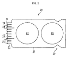
- the TAB sheet 20 of this embodiment comprises a copper plate 21 arranged on an electrically conductive layer and a polyimide resin layer 28 covering a part of the copper plate 21 for insulation thereof.
- the TAB sheet 20 may comprise an insulant plate with an electrically conductive layer formed thereon in place of the copper plate 21.
- openings 26 and 27 are formed in the TAB sheet 20 at positions to respectively correspond to those of the openings 16 and 17 formed in the cooling assembly 10.
- the TAB sheet 20 has a reduced-width portion in the vicinity of one end thereof where several slits 24 and 25 are formed.
- the slits 24 are formed not to extend to the end of the sheet 20 and the slits 25 are formed to extend to the end of the sheet 20.
- the Slits 24 and 25 are formed for preventing stress on the LD bar 60 due to the bonding so that the extending section 22 does not lose its webbed form.
- an appropriate region of the reduced-width portion of the TAB sheet 20 forms a webbed extending section 22 of the copper plate 21 not coated with the polyimide resin layer 28.
- a terminal portion of the extending section 22 of the TAB sheet 20 is used as a connecting portion 23 for bonding with the other electrode of the LD bar 60.
- the Slits 24 and 25 are formed so that the extending section 22 does not lose its webbed form.
- a part or the whole of the copper plate 21 including the connecting portion 23 is coated by tin-lead solder.
- the connecting portion 23 may be further coated by gold in addition to the tin-lead solder so as to secure higher electrical conductivity.
- a conductive path having a sectional area larger than the bonding wire is formed by the copper plate 21 of the TAB sheet 20 to realize a low electrical resistance at a relatively low cost.
- the conventional wiring structure in which the connection board 52, the insulating sheet 51 and the gold wire 53 are used, as shown in FIG. 5, is replaced with the TAB sheet 20 having the webbed extending section 22 to make the whole wiring structure simple and also reduce the manufacturing cost.
- the copper plate 21 of the TAB sheet 20 also functions as the connection board 52 of the conventional structure to realize the structure directly electrically connecting the LD bar 60 and the connection board 52 to contribute reduction of electrical resistance of the wiring structure.
- a guide or a pin hole may be formed in the cooling assembly 10 for easier positioning in stacking the light-emitting units P1-P N .
- a guide 29 as shown in FIG. 2 or a pin hole for positioning may be formed in the TAB sheet 20 to correspond the guide or the pin hole formed in the cooling assembly 10.
- the TAB tape forming the TAB sheet 20 is a mass-produced product having a standard thickness
- the TAB tape has a restriction in selecting the thickness in view of the advantage in its cost.
- a necessary space for arranging the LD bar 60 is secured between the adjacent cooling assemblies by providing a spacer plate.
- the TAB sheet 20 is arranged such that the polyimide resin layer 28 confronts the metal plate 13 of the cooling assembly 10, and a spacer plate 31 is intervened between the TAB sheet 20 and the metal plate 13.
- the spacer plate 31 is used for adjusting a level of the TAB sheet 20 to conform to a level of the LD bar 60.
- the spacer plate 31 may be omitted if it is not necessary to adjust the level of the TAB sheet 20.
- the level adjustment is carried out such that an appropriate space is formed between the connection portion 23 of the TAB sheet 20 positioned on the LD bar 60 and the metal plate 11 of the cooling assembly of the adjacent light-emitting unit Pn+1 to prevent the connection portion 23 from being in contact with the metal plate 11 not to exert an external force on the LD bar 60, when the light-emitting units P1-P N are stacked.
- the copper plate 21 of the TAB sheet 20 is electrically isolated from the cooling assembly 10 of the light-emitting unit Pn by the polyimide resin layer 28 of the TAB sheet 20 positioned therebetween, and therefore the insulating sheet 51 used in the conventional structure as shown in FIG. 5 is made unnecessary.
- the spacer plate 31 may be either electrically conductive or not electrically conductive and it is preferable that the spacer plate 31 presents adhesion with heat so as to obtain stable fixing state of the spacer plate 31 without any special fixing means.
- a metal plate coated with a solder layer having an appropriate melting point to present the adhesion with heat is preferably used as the spacer plate 31.
- the outer surface of the copper plate 21 opposite to a surface coated by the polyimide resin layer 28 is in contact and electrically connected with the metal plate 11 of the cooling assembly 10 of the adjacent light-emitting unit Pn+1.
- a part or the whole of the surface of the metal plate 11 and 13 of the cooling assembly 10 may be coated with solder.
- the cooling assembly 10 serves as one electrode (e.g., a positive electrode) of the light-emitting unit Pn
- the copper plate 21 of the TAB tape 20 serves as the other electrode (e.g., a negative electrode to be connected to earth) of the light-emitting unit Pn.
- the plurality of light-emitting units P1-P N are successively stacked to form the light-emitting device so that the LD bars 60 of the light-emitting units P1-P N are electrically connected in series to be driven by the driving current.
- One terminal (e.g., positive terminal) of a power source is connected to the cooling assembly 10 of the light-emitting unit P1 at one end of the light-emitting device and the other terminal (e.g., negative terminal) of the power source is connected to the copper plate 21 of the light-emitting device PN at the other end of the light-emitting device.
- Openings respectively corresponding to the openings 16 and 17 formed in the metal plates 11-13 of the cooling assembly 10 are formed in the spacer plate 31, so that the passages of the coolant are formed through the stacked light-emitting units P1-PN.
- One end or both ends of each passage is connected to an inlet or an outlet of a circular pump of coolant.
- the TAB sheet 20 is arranged such that the polyimide resin layer 28 thereof confronts the cooling assembly 10 of the light-emitting unit Pn and the spacer plate 31 is intervened between the TAB sheet 20 and the cooling assembly 10 of the light-emitting unit Pn.
- the spacer plate 31 may be arranged between the TAB sheet 20 and the cooling assembly 10 of the adjacent light-emitting unit Pn+1. Such arrangement is shown in FIG. 3 as a second embodiment.
- FIG. 3 only three adjacent light-emitting units, a light-emitting unit Qn-1, a light-emitting unit Qn and a light-emitting unit Qn+1 (n: integer not less than two) are depicted in light-emitting units Q1-Q N which constitute the surface light-emitting device.
- the light-emitting unit Qn comprises a LD bar 60 and a cooling assembly 10 for cooling the LD bar 60 mounted thereon.
- a cooling assembly having a conventional structure may be adopted as the cooling assembly 10 as shown in an exploded view of FIG. 4.
- the cooling assembly 10 comprises three metal plates 11-13 joined together, which have openings 16 and 17 formed at corresponding positions to form passages for supplying/discharging the coolant.
- the coolant supplied from the openings 16 flows through coolant paths 15 formed by grooves and through holes in the metal plates 11-13 and discharged from the openings 17.
- the LD bar 60 is mounted on an electrically conductive die spacer 41 fixed on the metal plate 13 by soldering in the vicinity of a peripheral side thereof, so that one electrode (e.g., positive electrode) of the LD bar 60 is electrically connected to the die spacer 41.
- a solder layer 43 is formed between the metal plate 13 and the die spacer 41, and a solder layer 42 is formed between the die spacer 41 and the LD bar 60 by the soldering.
- a TAB sheet 20 formed from a TAB tape is used for electrically connecting the other electrode (e.g., negative electrode) of the LD bar 60 with the metal plate 11 of the adjacent light-emitting unit Qn+1.
- the TAB sheet 20 may have the same structure in the first embodiment.
- the TAB sheet 20 comprises a copper plate 21 and a polyimide resin layer 28 covering a part of the copper plate 21, and has openings 26 and 27 respectively corresponding to the openings 16 and 17 formed in the cooling assembly 10.
- the TAB sheet 20 has a reduced-width portion in the vicinity of one end thereof where several slits 24 and 25 are formed.
- a terminal portion of an extending section 22 of the copper plate 21 not coated with the polyimide resin layer 28 in the reduced-width portion of the TAB sheet 20 is used as a connecting portion 23 for bonding with the other electrode of the LD bar 60. It is preferable that a part or the whole of the copper plate 21 including the connecting portion 23 is coated by tin-lead solder. The connecting portion 23 may be further coated by gold in addition to the tin-lead solder so as to secure higher electrical conductivity.
- a spacer plate 32 is intervened between the copper layer of the TAB sheet 20 and the metal plate 11 of the cooling assembly 10 of the adjacent cooling assembly Qn+1.
- the spacer plate 32 is arranged for adjusting a distance between the cooling assembly 10 of the light-emitting unit Qn and the cooling assembly 10 of the adjacent light-emitting unit Qn+1 so that the connecting portion 23 of the TAB sheet 20 is not in contact with the cooling assembly 10 of the adjacent light-emitting unit Qn+1 when the light-emitting units P1-P N are stacked.
- the spacer plate 32 may be omitted if it is not necessary to adjust the distance between the cooling assemblies 10.
- the polyimide resin layer 28 of the TAB sheet 20 is confronting and in contact with the cooling assembly 10 of the light-emitting unit Qn without any member intervened therebetween in both cases of using and not using the spacer plate 32.
- the copper plate 21 of the TAB sheet 20 is electrically isolated from the cooling assembly 10 of the light-emitting unit Qn by the polyimide layer 28 by high insulating characteristic of polyimide resin.
- the insulating sheet 51 used in the conventional structure as shown in FIG. 5 is made unnecessary.
- the spacer plate 32 is required to have a function of securing the electrical conductivity between the copper plate 21 and the cooling assembly 10 of the adjacent light-emitting unit Qn+1.
- the spacer plate 32 is made of an electrically conductive material or an insulating material coated with an electrically conductive material. Typical electrical conductive materials are copper and an alloy of copper and tungsten.
- surfaces of the spacer plate 32 particularly, surfaces in contact with the adjacent cooling assembly 10 and the TAB sheet 20, respectively, may be coated by solder.
- an electrically conductive film or an electrically conductive double-coated adhesive tape winch presents adhesion by heat may be used as the spacer plate 32.
- a part of the cooling assembly 10 of each light-emitting unit serves as one electrode (e.g., a positive electrode) of the light-emitting unit
- the copper plate 21 of the TAB sheet 20 serves as the other electrode (e.g., a negative electrode to be connected to the ground) of the light-emitting unit.
- the plurality of light-emitting units Q1-Q N are successively stacked and the LD bars 60 of the light-emitting units Q1-Q N are electrically connected in series so that driving current flows in the LD bars 60 in series.
- One terminal (e.g., positive terminal) of a power source is connected to the cooling assembly 10 of the light-emitting unit P1 at one end of the light-emitting device and the other terminal (e.g., negative terminal) of the power source is connected to the copper plate 21 of the light-emitting device PN at the other end of the light-emitting device.
- Openings respectively corresponding to the openings 16 and 17 formed in the metal plates 11-13 of the cooling assembly 10 are formed in the spacer plate 32, so that the passages of the coolant are formed through the stacked light-emitting units Q1-QN.
- One end or both ends of each passage is connected to an inlet or an outlet of a circular pump of coolant.
- soldering material of Pb-Sn containing Sn at a composition ratio of 80% is generally used at low cost.
- the insulating sheet, the conductive sheet and the bonding wire used for the electrical connection with the LD bar in the conventional structure are replaced with the TAB sheet formed from the TAB tape which is a mass-produced product available at low cost, to reduce the cost of the parts and cost of assembly of the surface light-emitting device.
- the TAB sheet has a large sectional area of the conductive part and the electrode of the LD bar and the cooling assembly is electrically connected by an integral conductive element of the conductive layer of the TAB sheet without connection board used in the conventional structure, to reduce electrical resistance in the electrical connection.
- an efficiency of energy conversion from electricity to light is enhanced to enable reduction of the driving voltage.
- the restriction of thickness of the TAB tape is coped-with by a spacer plate for adjusting the space between the adjacent cooling assemblies to utilize the merit of mass-production of the TAB tape.
- Gold or solder coating is provided on necessary portions of the elements to secure stable bonding and electrical conductivity between the elements.
- the stress possibly caused by the web-like conductive layer of the TAB sheet is eliminated by the slits formed in the electrically connecting portion of the conductive layer. Further, the guide and the holes for pins make the stacking of the light-emitting unit easy.
Landscapes
- Physics & Mathematics (AREA)
- Condensed Matter Physics & Semiconductors (AREA)
- General Physics & Mathematics (AREA)
- Electromagnetism (AREA)
- Optics & Photonics (AREA)
- Semiconductor Lasers (AREA)
Claims (20)
- Zweidimensionale Lichtemissionsvorrichtung, umfassend:eine Anzahl gestapelte Lichtemissionseinheiten (Pn-1, Pn, Pn + 1; Qn-1, Qn, Qn + 1) mit jeweils einer Kühleinrichtung (10) und einem Laserdiodenbarren (60), der auf der Kühleinrichtung angeordnet und thermisch und elektrisch mit der Kühleinrichtung verbunden ist, wobei mindestens ein Teil (13) der Kühleinrichtung (10) als erste Elektrode ihrer Lichtemissionseinheit dient, wobei die Vorrichtung dadurch gekennzeichnet ist, dassjede der Anzahl Lichtemissionseinheiten zudem eine Tape-Automated-Bonding-Schicht (20) besitzt mit einer elektrisch leitfähigen Schicht (21) und einer Isolierschicht (28), die zwischen benachbarten Kühleinrichtungen (10) angeordnet ist, so dass die Isolierschicht einer Oberfläche der Kühleinrichtung gegenüberliegt, auf der der Laserdiodenbarren (60) angeordnet ist, wobei die elektrisch leitfähige Schicht für die elektrische Verbindung mit dem Laserdiodenbarren einen verrippten Verlängerungsabschnitt (22) besitzt, der als zweite Elektrode seiner Lichtemissionseinheit dient, wobei die erste Elektrode und die zweite Elektrode durch die Isolierschicht (28) voneinander elektrisch isoliert sind.
- Zweidimensionale Lichtemissionsvorrichtung nach Anspruch 1, wobei jede Kühleinrichtung (10) Öffnungen (16, 17) hat, die Durchlässe zum Ein- und Auslassen von Kühlmittel bilden, sowie Kühlmittelpfade, die mit den Durchlässen kommunizieren, und jede Tape-Automated-Bonding-Schicht (20) Öffnungen (26, 27) hat, die den Öffnungen in der Kühleinrichtung entsprechen.
- Zweidimensionale Lichtemissionsvorrichtung nach Anspruch 1 oder 2, wobei jede Lichtemissionseinheit (Pn-1, Pn, Pn + 1; Qn-1, Qn, Qn + 1) zudem eine Abstandshalterplatte (31, 32) zum Einstellen eines Abstands zwischen benachbarten Kühleinrichtungen besitzt.
- Zweidimensionale Lichtemissionsvorrichtung nach Anspruch 3, wobei die Abstandshalterplatte (31) zwischen der Tape-Automated-Bonding-Schicht (20) und der Oberfläche der Kühleinrichtung (10) ihrer Lichtemissionseinheit (Pn-1, Pn, Pn + 1) angeordnet ist.
- Zweidimensionale Lichtemissionsvorrichtung nach Anspruch 3 oder 4, wobei die Abstandshalterplatte (31, 32) aus einem Bauteil besteht, das bei Wärme Haftung aufweist.
- Zweidimensionale Lichtemissionsvorrichtung nach Anspruch 3, wobei die Abstandshalterplatte (32) zwischen der Tape-Automated-Bonding-Schicht (20) ihrer Lichtemissionseinheit (Qn) und der Kühleinrichtung (10) der Lichtemissionseinheit (Qn + 1) neben ihrer Lichtemissionseinheit angeordnet ist.
- Zweidimensionale Lichtemissionsvorrichtung nach einem der Ansprüche 3 bis 6, wobei die Abstandshalterplatte (31, 32) aus elektrisch leitfähigem Material besteht.
- Zweidimensionale Lichtemissionsvorrichtung nach Anspruch 7, wobei die Abstandshalterplatte (31, 32) aus Kupfer besteht.
- Zweidimensionale Lichtemissionsvorrichtung nach Anspruch 7, wobei die Abstandshalterplatte (31, 32) aus einer Kupfer und Wolfram enthaltenden Legierung besteht.
- Zweidimensionale Lichtemissionsvorrichtung nach einem der Ansprüche 3 bis 6, wobei die Abstandshalterplatte (31, 32) aus einem Bauteil besteht, das aus einem lsoliermaterial, beschichtet mit elektrisch leitfähigem Material, hergestellt ist.
- Zweidimensionale Lichtemissionsvorrichtung nach Anspruch 6 oder einem der Ansprüche 7 bis 10 im Anschluss an Anspruch 6, wobei zumindest eine Oberfläche der Abstandshalterplatte (32), die der Tape-Automated-Bonding-Schicht (20) ihrer Lichtemissionseinheit (Qn) gegenüberliegt, und eine Oberfläche der Abstandshalterplatte, die der Kühleinrichtung (10) der Lichtemissionseinheit (Qn + 1) neben ihrer Lichtemissionseinheit gegenüberliegt, mit Lötmittel beschichtet sind.
- Zweidimensionale Lichtemissionsvorrichtung nach einem vorhergehenden Anspruch, wobei die Tape-Automated-Bonding-Schicht (20) zudem eine Metallplatte enthält, die auf der elektrisch leitfähigen Schicht (21) angeordnet ist.
- Zweidimensionale Lichtemissionsvorrichtung nach Anspruch 12, wobei die Metallplatte eine Kupferplatte ist.
- Zweidimensionale Lichtemissionsvorrichtung nach Anspruch 13, wobei die Kupferplatte mit Lötmittel beschichtet ist.
- Zweidimensionale Lichtemissionsvorrichtung nach einem der Ansprüche 1 bis 11, wobei die Tape-Automated-Bonding-Schicht (20) zudem eine Isoliermaterialplatte enthält mit einer darauf gebildeten elektrisch leitfähigen Schicht (21).
- Zweidimensionale Lichtemissionsvorrichtung nach einem vorhergehenden Anspruch, wobei ein mit dem Laserdiodenbarren (60) elektrisch zu verbindender Verbindungsabschnitt (23) des Verlängerungsabschnitts (23) der Tape-Automated-Bonding-Schicht (20) mit Lötmittel oder Gold beschichtet ist.
- Zweidimensionale Lichtemissionsvorrichtung nach einem vorhergehenden Anspruch, wobei Schlitze (24, 25) in der Nähe eines mit dem Laserdiodenbarren (60) elektrisch zu verbindenden Verbindungsabschnitts (23) des Verlängerungsabschnitts (23) der Tape-Automated-Bonding-Schicht (20) ausgebildet sind.
- Zweidimensionale Lichtemissionsvorrichtung nach einem vorhergehenden Anspruch, wobei Außenflächen der Kühleinrichtungen (10) mit Gold beschichtet sind.
- Zweidimensionale Lichtemissionsvorrichtung nach einem vorhergehenden Anspruch, wobei jede Lichtemissionseinheit (Pn-1, Pn, Pn + 1; Qn-1, Qn, Qn + 1) zudem einen Düsenabstandshalter (41) besitzt, der sich zwischen dem Laserdiodenbarren (60) und der Kühleinrichtung (10) befindet.
- Zweidimensionale Lichtemissionsvorrichtung nach Anspruch 19, wobei der Düsenabstandshalter (41) aus einem Material besteht mit einem Wärmeausdehnungskoeffizienten, der annähernd dem Wärmeausdehnungskoeffizienten des Laserdiodenbarrens (60) entspricht, und mit hoher Wärmeleitfähigkeit.
Applications Claiming Priority (2)
| Application Number | Priority Date | Filing Date | Title |
|---|---|---|---|
| JP2001250314A JP3643328B2 (ja) | 2001-08-21 | 2001-08-21 | 2次元ldアレイ発光装置 |
| JP2001250314 | 2001-08-21 |
Publications (3)
| Publication Number | Publication Date |
|---|---|
| EP1286441A2 EP1286441A2 (de) | 2003-02-26 |
| EP1286441A3 EP1286441A3 (de) | 2004-01-02 |
| EP1286441B1 true EP1286441B1 (de) | 2006-11-08 |
Family
ID=19079162
Family Applications (1)
| Application Number | Title | Priority Date | Filing Date |
|---|---|---|---|
| EP02255655A Expired - Lifetime EP1286441B1 (de) | 2001-08-21 | 2002-08-14 | Zwei-dimensionaler Vielfachdiodenlaser |
Country Status (4)
| Country | Link |
|---|---|
| US (1) | US6934309B2 (de) |
| EP (1) | EP1286441B1 (de) |
| JP (1) | JP3643328B2 (de) |
| DE (1) | DE60215892T2 (de) |
Cited By (1)
| Publication number | Priority date | Publication date | Assignee | Title |
|---|---|---|---|---|
| RU2712764C1 (ru) * | 2019-06-11 | 2020-01-31 | Федеральное государственное бюджетное учреждение науки Физический институт им. П.Н. Лебедева Российской академии наук (ФИАН) | Способ создания двумерной матрицы лазерных диодов и двумерная матрица лазерных диодов |
Families Citing this family (32)
| Publication number | Priority date | Publication date | Assignee | Title |
|---|---|---|---|---|
| JP4934954B2 (ja) * | 2003-10-15 | 2012-05-23 | 日亜化学工業株式会社 | ヒートシンク及びヒートシンクを備えた半導体装置 |
| JP4654664B2 (ja) * | 2004-01-13 | 2011-03-23 | セイコーエプソン株式会社 | 光源装置および投射型表示装置 |
| JP4600733B2 (ja) * | 2004-07-12 | 2010-12-15 | ソニー株式会社 | 半導体レーザ装置およびその製造方法 |
| JP2007019265A (ja) * | 2005-07-07 | 2007-01-25 | Sony Corp | 発光装置 |
| RU2347104C2 (ru) * | 2006-05-12 | 2009-02-20 | ООО "ГРЦ-Вертикаль" | Ротор ветряной установки с вертикальной осью вращения (варианты) |
| DE102006051745B4 (de) * | 2006-09-28 | 2024-02-08 | OSRAM Opto Semiconductors Gesellschaft mit beschränkter Haftung | LED-Halbleiterkörper und Verwendung eines LED-Halbleiterkörpers |
| JP2008139279A (ja) * | 2006-11-02 | 2008-06-19 | Kyoto Denkiki Kk | 照明装置 |
| DE102007009380A1 (de) * | 2007-02-21 | 2008-09-04 | Forschungsverbund Berlin E.V. | Impulslaser und Verfahren zur Erzeugung von Laserstrahlung |
| DE102007016772A1 (de) * | 2007-04-04 | 2008-10-16 | Jenoptik Laserdiode Gmbh | Stapelbare mehrschichtige Mikrokanalwärmesenke |
| JP2008300596A (ja) * | 2007-05-31 | 2008-12-11 | Sony Corp | ヒートシンクおよび半導体レーザ装置 |
| US7623560B2 (en) * | 2007-09-27 | 2009-11-24 | Ostendo Technologies, Inc. | Quantum photonic imagers and methods of fabrication thereof |
| DE102008026229B4 (de) | 2008-05-29 | 2012-12-27 | Jenoptik Laser Gmbh | Wärmeübertragungsvorrichtung zur doppelseitigen Kühlung eines Halbleiterbauelementes |
| DE102008036439A1 (de) * | 2008-08-05 | 2010-02-11 | Jenoptik Laserdiode Gmbh | Wärmeableitmodul mit einem Halbleiterelement und Herstellungsverfahren für ein solches Wärmeableitmodul |
| CN103650129A (zh) * | 2011-05-19 | 2014-03-19 | 港大科桥有限公司 | 芯片堆叠 |
| JP2012248812A (ja) * | 2011-05-31 | 2012-12-13 | Sumitomo Electric Ind Ltd | 半導体光集積素子の製造方法 |
| US8787414B1 (en) * | 2011-09-07 | 2014-07-22 | Science Research Laboratory, Inc. | Methods and systems for providing a low stress electrode connection |
| CN104485576A (zh) * | 2014-12-12 | 2015-04-01 | 中国工程物理研究院流体物理研究所 | 一种多芯组高功率塑封脉冲半导体激光二极管 |
| KR102406606B1 (ko) * | 2015-10-08 | 2022-06-09 | 삼성디스플레이 주식회사 | 유기 발광 소자, 이를 포함하는 유기 발광 표시 장치, 및 이의 제조 방법 |
| CN108604768B (zh) * | 2016-04-19 | 2020-03-24 | 松下知识产权经营株式会社 | 半导体激光器装置及其制造方法 |
| CN106684707A (zh) * | 2017-03-13 | 2017-05-17 | 西安炬光科技股份有限公司 | 一种粘接型半导体激光器叠阵及其制备方法 |
| US12100696B2 (en) | 2017-11-27 | 2024-09-24 | Seoul Viosys Co., Ltd. | Light emitting diode for display and display apparatus having the same |
| US10892296B2 (en) | 2017-11-27 | 2021-01-12 | Seoul Viosys Co., Ltd. | Light emitting device having commonly connected LED sub-units |
| US11527519B2 (en) | 2017-11-27 | 2022-12-13 | Seoul Viosys Co., Ltd. | LED unit for display and display apparatus having the same |
| US11282981B2 (en) * | 2017-11-27 | 2022-03-22 | Seoul Viosys Co., Ltd. | Passivation covered light emitting unit stack |
| US10892297B2 (en) * | 2017-11-27 | 2021-01-12 | Seoul Viosys Co., Ltd. | Light emitting diode (LED) stack for a display |
| US10748881B2 (en) | 2017-12-05 | 2020-08-18 | Seoul Viosys Co., Ltd. | Light emitting device with LED stack for display and display apparatus having the same |
| US10886327B2 (en) | 2017-12-14 | 2021-01-05 | Seoul Viosys Co., Ltd. | Light emitting stacked structure and display device having the same |
| US11552057B2 (en) | 2017-12-20 | 2023-01-10 | Seoul Viosys Co., Ltd. | LED unit for display and display apparatus having the same |
| US11522006B2 (en) | 2017-12-21 | 2022-12-06 | Seoul Viosys Co., Ltd. | Light emitting stacked structure and display device having the same |
| US11552061B2 (en) | 2017-12-22 | 2023-01-10 | Seoul Viosys Co., Ltd. | Light emitting device with LED stack for display and display apparatus having the same |
| US11114499B2 (en) | 2018-01-02 | 2021-09-07 | Seoul Viosys Co., Ltd. | Display device having light emitting stacked structure |
| US10784240B2 (en) | 2018-01-03 | 2020-09-22 | Seoul Viosys Co., Ltd. | Light emitting device with LED stack for display and display apparatus having the same |
Family Cites Families (2)
| Publication number | Priority date | Publication date | Assignee | Title |
|---|---|---|---|---|
| US4716568A (en) * | 1985-05-07 | 1987-12-29 | Spectra Diode Laboratories, Inc. | Stacked diode laser array assembly |
| US6274391B1 (en) * | 1992-10-26 | 2001-08-14 | Texas Instruments Incorporated | HDI land grid array packaged device having electrical and optical interconnects |
-
2001
- 2001-08-21 JP JP2001250314A patent/JP3643328B2/ja not_active Expired - Fee Related
-
2002
- 2002-08-12 US US10/216,324 patent/US6934309B2/en not_active Expired - Fee Related
- 2002-08-14 EP EP02255655A patent/EP1286441B1/de not_active Expired - Lifetime
- 2002-08-14 DE DE60215892T patent/DE60215892T2/de not_active Expired - Fee Related
Cited By (1)
| Publication number | Priority date | Publication date | Assignee | Title |
|---|---|---|---|---|
| RU2712764C1 (ru) * | 2019-06-11 | 2020-01-31 | Федеральное государственное бюджетное учреждение науки Физический институт им. П.Н. Лебедева Российской академии наук (ФИАН) | Способ создания двумерной матрицы лазерных диодов и двумерная матрица лазерных диодов |
Also Published As
| Publication number | Publication date |
|---|---|
| US20030039278A1 (en) | 2003-02-27 |
| DE60215892D1 (de) | 2006-12-21 |
| EP1286441A2 (de) | 2003-02-26 |
| JP2003060283A (ja) | 2003-02-28 |
| EP1286441A3 (de) | 2004-01-02 |
| US6934309B2 (en) | 2005-08-23 |
| DE60215892T2 (de) | 2007-03-01 |
| JP3643328B2 (ja) | 2005-04-27 |
Similar Documents
| Publication | Publication Date | Title |
|---|---|---|
| EP1286441B1 (de) | Zwei-dimensionaler Vielfachdiodenlaser | |
| JP4009056B2 (ja) | パワーモジュール | |
| US6498355B1 (en) | High flux LED array | |
| US7391153B2 (en) | Light emitting device provided with a submount assembly for improved thermal dissipation | |
| JP3847691B2 (ja) | 電力用半導体装置 | |
| US7985975B2 (en) | Light emitting package and light emitting package array formed by coupled electrodes | |
| US20210057878A1 (en) | Semiconductor laser device | |
| US7058101B2 (en) | Stepped manifold array of microchannel heat sinks | |
| US4719631A (en) | Conductively cooled laser diode array pumped laser | |
| EP3159981A1 (de) | Thermisch leitendes, stromführendes, elektrisch isoliertes submount für laserdioden-arrays | |
| EP0777275A2 (de) | Halbleitermodul mit Kühlkörper | |
| JP2005158957A (ja) | 発光装置 | |
| US20020110165A1 (en) | Method and system for cooling at least one laser diode with a cooling fluid | |
| US20070200223A1 (en) | Semiconductor device and semiconductor module therewith | |
| US7026712B2 (en) | Peltier module with durable power supply lines and exothermic module with built-in cooler | |
| EP1341275B1 (de) | Lasermodul | |
| CN114530757A (zh) | 光半导体模块 | |
| JP2009246053A (ja) | フレーム板を備えたダイオード | |
| JP2003078177A (ja) | 熱電装置 | |
| KR20230105364A (ko) | 세라믹 기판 유닛 및 그 제조방법 | |
| US6600223B2 (en) | Hermetically sealing enclosure for housing photo-semiconductor devices and photo-semiconductor module incorporating the enclosure | |
| KR102882290B1 (ko) | 세라믹 기판 유닛 및 그 제조방법 | |
| CN119673910B (zh) | 一种层叠式氮化硅陶瓷的碳化硅芯片模块封装 | |
| CN221009484U (zh) | 一种光电器件的封装模块及光电模组 | |
| CN218569494U (zh) | 单电极陶瓷热沉及半导体激光器热沉装置 |
Legal Events
| Date | Code | Title | Description |
|---|---|---|---|
| PUAI | Public reference made under article 153(3) epc to a published international application that has entered the european phase |
Free format text: ORIGINAL CODE: 0009012 |
|
| AK | Designated contracting states |
Kind code of ref document: A2 Designated state(s): AT BE BG CH CY CZ DE DK EE ES FI FR GB GR IE IT LI LU MC NL PT SE SK TR Designated state(s): AT BE BG CH CY CZ DE DK EE ES FI FR GB GR IE IT LI LU MC NL PT SE SK TR |
|
| AX | Request for extension of the european patent |
Extension state: AL LT LV MK RO SI |
|
| PUAL | Search report despatched |
Free format text: ORIGINAL CODE: 0009013 |
|
| AK | Designated contracting states |
Kind code of ref document: A3 Designated state(s): AT BE BG CH CY CZ DE DK EE ES FI FR GB GR IE IT LI LU MC NL PT SE SK TR |
|
| AX | Request for extension of the european patent |
Extension state: AL LT LV MK RO SI |
|
| RAP1 | Party data changed (applicant data changed or rights of an application transferred) |
Owner name: FANUC LTD |
|
| 17P | Request for examination filed |
Effective date: 20040628 |
|
| AKX | Designation fees paid |
Designated state(s): DE |
|
| 17Q | First examination report despatched |
Effective date: 20040901 |
|
| GRAP | Despatch of communication of intention to grant a patent |
Free format text: ORIGINAL CODE: EPIDOSNIGR1 |
|
| GRAS | Grant fee paid |
Free format text: ORIGINAL CODE: EPIDOSNIGR3 |
|
| GRAA | (expected) grant |
Free format text: ORIGINAL CODE: 0009210 |
|
| AK | Designated contracting states |
Kind code of ref document: B1 Designated state(s): DE |
|
| REF | Corresponds to: |
Ref document number: 60215892 Country of ref document: DE Date of ref document: 20061221 Kind code of ref document: P |
|
| PLBE | No opposition filed within time limit |
Free format text: ORIGINAL CODE: 0009261 |
|
| STAA | Information on the status of an ep patent application or granted ep patent |
Free format text: STATUS: NO OPPOSITION FILED WITHIN TIME LIMIT |
|
| 26N | No opposition filed |
Effective date: 20070809 |
|
| PG25 | Lapsed in a contracting state [announced via postgrant information from national office to epo] |
Ref country code: DE Free format text: LAPSE BECAUSE OF NON-PAYMENT OF DUE FEES Effective date: 20080301 |