EP1286532A1 - Fehlerdiffusion für eine digitale Abbildungsvorrichtung - Google Patents
Fehlerdiffusion für eine digitale Abbildungsvorrichtung Download PDFInfo
- Publication number
- EP1286532A1 EP1286532A1 EP02102113A EP02102113A EP1286532A1 EP 1286532 A1 EP1286532 A1 EP 1286532A1 EP 02102113 A EP02102113 A EP 02102113A EP 02102113 A EP02102113 A EP 02102113A EP 1286532 A1 EP1286532 A1 EP 1286532A1
- Authority
- EP
- European Patent Office
- Prior art keywords
- value
- error
- binary
- quantization
- bit
- Prior art date
- Legal status (The legal status is an assumption and is not a legal conclusion. Google has not performed a legal analysis and makes no representation as to the accuracy of the status listed.)
- Withdrawn
Links
- 238000009792 diffusion process Methods 0.000 title claims description 17
- 238000003384 imaging method Methods 0.000 title claims description 11
- 238000013139 quantization Methods 0.000 claims abstract description 61
- 238000000034 method Methods 0.000 claims abstract description 11
- 238000001914 filtration Methods 0.000 claims description 3
- 238000010586 diagram Methods 0.000 description 4
- 238000006243 chemical reaction Methods 0.000 description 3
- 230000004075 alteration Effects 0.000 description 1
- 230000008901 benefit Effects 0.000 description 1
- 230000008859 change Effects 0.000 description 1
- 239000004973 liquid crystal related substance Substances 0.000 description 1
- 230000008569 process Effects 0.000 description 1
- 230000009467 reduction Effects 0.000 description 1
- 238000006467 substitution reaction Methods 0.000 description 1
Images

Classifications
-
- G—PHYSICS
- G09—EDUCATION; CRYPTOGRAPHY; DISPLAY; ADVERTISING; SEALS
- G09G—ARRANGEMENTS OR CIRCUITS FOR CONTROL OF INDICATING DEVICES USING STATIC MEANS TO PRESENT VARIABLE INFORMATION
- G09G3/00—Control arrangements or circuits, of interest only in connection with visual indicators other than cathode-ray tubes
- G09G3/20—Control arrangements or circuits, of interest only in connection with visual indicators other than cathode-ray tubes for presentation of an assembly of a number of characters, e.g. a page, by composing the assembly by combination of individual elements arranged in a matrix no fixed position being assigned to or needed to be assigned to the individual characters or partial characters
- G09G3/34—Control arrangements or circuits, of interest only in connection with visual indicators other than cathode-ray tubes for presentation of an assembly of a number of characters, e.g. a page, by composing the assembly by combination of individual elements arranged in a matrix no fixed position being assigned to or needed to be assigned to the individual characters or partial characters by control of light from an independent source
-
- G—PHYSICS
- G09—EDUCATION; CRYPTOGRAPHY; DISPLAY; ADVERTISING; SEALS
- G09G—ARRANGEMENTS OR CIRCUITS FOR CONTROL OF INDICATING DEVICES USING STATIC MEANS TO PRESENT VARIABLE INFORMATION
- G09G3/00—Control arrangements or circuits, of interest only in connection with visual indicators other than cathode-ray tubes
- G09G3/20—Control arrangements or circuits, of interest only in connection with visual indicators other than cathode-ray tubes for presentation of an assembly of a number of characters, e.g. a page, by composing the assembly by combination of individual elements arranged in a matrix no fixed position being assigned to or needed to be assigned to the individual characters or partial characters
- G09G3/2007—Display of intermediate tones
- G09G3/2059—Display of intermediate tones using error diffusion
-
- G—PHYSICS
- G09—EDUCATION; CRYPTOGRAPHY; DISPLAY; ADVERTISING; SEALS
- G09G—ARRANGEMENTS OR CIRCUITS FOR CONTROL OF INDICATING DEVICES USING STATIC MEANS TO PRESENT VARIABLE INFORMATION
- G09G2340/00—Aspects of display data processing
- G09G2340/04—Changes in size, position or resolution of an image
- G09G2340/0407—Resolution change, inclusive of the use of different resolutions for different screen areas
- G09G2340/0428—Gradation resolution change
-
- G—PHYSICS
- G09—EDUCATION; CRYPTOGRAPHY; DISPLAY; ADVERTISING; SEALS
- G09G—ARRANGEMENTS OR CIRCUITS FOR CONTROL OF INDICATING DEVICES USING STATIC MEANS TO PRESENT VARIABLE INFORMATION
- G09G3/00—Control arrangements or circuits, of interest only in connection with visual indicators other than cathode-ray tubes
- G09G3/20—Control arrangements or circuits, of interest only in connection with visual indicators other than cathode-ray tubes for presentation of an assembly of a number of characters, e.g. a page, by composing the assembly by combination of individual elements arranged in a matrix no fixed position being assigned to or needed to be assigned to the individual characters or partial characters
- G09G3/2007—Display of intermediate tones
- G09G3/2018—Display of intermediate tones by time modulation using two or more time intervals
- G09G3/2022—Display of intermediate tones by time modulation using two or more time intervals using sub-frames
- G09G3/2029—Display of intermediate tones by time modulation using two or more time intervals using sub-frames the sub-frames having non-binary weights
-
- G—PHYSICS
- G09—EDUCATION; CRYPTOGRAPHY; DISPLAY; ADVERTISING; SEALS
- G09G—ARRANGEMENTS OR CIRCUITS FOR CONTROL OF INDICATING DEVICES USING STATIC MEANS TO PRESENT VARIABLE INFORMATION
- G09G3/00—Control arrangements or circuits, of interest only in connection with visual indicators other than cathode-ray tubes
- G09G3/20—Control arrangements or circuits, of interest only in connection with visual indicators other than cathode-ray tubes for presentation of an assembly of a number of characters, e.g. a page, by composing the assembly by combination of individual elements arranged in a matrix no fixed position being assigned to or needed to be assigned to the individual characters or partial characters
- G09G3/34—Control arrangements or circuits, of interest only in connection with visual indicators other than cathode-ray tubes for presentation of an assembly of a number of characters, e.g. a page, by composing the assembly by combination of individual elements arranged in a matrix no fixed position being assigned to or needed to be assigned to the individual characters or partial characters by control of light from an independent source
- G09G3/3433—Control arrangements or circuits, of interest only in connection with visual indicators other than cathode-ray tubes for presentation of an assembly of a number of characters, e.g. a page, by composing the assembly by combination of individual elements arranged in a matrix no fixed position being assigned to or needed to be assigned to the individual characters or partial characters by control of light from an independent source using light modulating elements actuated by an electric field and being other than liquid crystal devices and electrochromic devices
- G09G3/346—Control arrangements or circuits, of interest only in connection with visual indicators other than cathode-ray tubes for presentation of an assembly of a number of characters, e.g. a page, by composing the assembly by combination of individual elements arranged in a matrix no fixed position being assigned to or needed to be assigned to the individual characters or partial characters by control of light from an independent source using light modulating elements actuated by an electric field and being other than liquid crystal devices and electrochromic devices based on modulation of the reflection angle, e.g. micromirrors
Definitions
- This invention relates to digital image processing, and more particularly to techniques for diffusing quantization error.
- quantization is the procedure of approximating continuous values with discrete values; in practice, the input values to the quantization procedure are often also discrete, but with a much finer resolution than that of the output values.
- the goal of quantization usually is to produce a more compact representation of the data while maintaining its usefulness for a certain purpose. For example, to store color intensities you can quantize floating-point values in the range [0.0, 1.0] to integer values in the range 0-255, representing them with 8 bits, which is considered a sufficient resolution for many applications dealing with color.
- the quantization is said to be uniform. Often, a nonuniform spacing is more appropriate when better resolution is needed over some parts of the range of values.
- quantization error A problem with quantization is quantization error, which can cause artifacts in the image.
- Various forms of dithering have been developed to reduce the perceptible results of quantization error.
- Error diffusion is a form of dithering in which quanitization errors are diffused to "future" pixels. Error diffusion attempts to spread the error locally. The argument is that, because the error appears close to where it should be, it need not become visible as an artifact in the picture. Originally intended for grayscale images, error diffusion may be extended to color images by error diffusing each of the three color planes independently.
- error diffusion reduces local quantization error by filtering the quantization error in a feedback loop.
- the objective is to balance the red, green, and blue components to make the result look as convincing as possible.
- the quantizer comprises an adder, a look up table, and an error diffusion filter.
- the adder adds an input value to a diffused error value, thereby producing an error-corrected input value.
- the look up table receives and converts the error-corrected input value to a non binary output value and determines the quantization error value.
- the error diffusion filter filters the quantization error and delivers the filtered, diffused error value to the adder.
- the quantization unit further comprises a multiplier, an adder, and a binary quantizer.
- the multiplier and adder are used to shift the input value so that non binary bits can be added to the output value, and the binary quantizer quantizes the appropriate bits of the output value.
- An advantage of the invention is that it can be used to provide non binary pixel values. These values can be used to optimize the operation of the imaging system, such as by providing pixel values that can displayed in time slices that conform to a minimum time slice available in a particular system.
- quantization unit a quantization unit
- DMD digital micro-mirror device
- FIGURE 3 An example of a DMD system that incorporates the quantization unit is explained below in connection with FIGURE 3.
- the principles described herein could also be applied to other digital imaging systems, both for printing and display.
- the invention is used for imaging systems in which data is displayed in accordance with time slices, and in which system limitations result in time slices that are not necessarily dictated by binary patterns.
- Examples of other imaging systems, with which the invention could be useful are spatial light modulator systems other than DMD systems, particularly display systems such as liquid crystal displays and other flat panel displays.
- image data is displayed in time slices, the minimum of which is a LSB time slice.
- Each frame of pixel data has a duration of 6 milliseconds, and for an 8-bit system in which quantization patterns are all binary, 255 LSB time slices are available.
- the fastest LSB time slice that can be actually used is 17 microseconds.
- FIGURE 1 illustrates a conventional quantization unit 10.
- Truncation error, e(x,y), processed by an error diffusion filter 11 is added to the incoming pixel value, In(x,y). This sum produces the error-compensated pixel, In'(x,y).
- the error-compensated pixel is then quantized by a quantizer 12, resulting in the output pixel, Out(x,y).
- the difference between the output pixel and the error-compensated pixel forms the new truncation error, e'(x,y), which is then processed by the error diffusion filter 11.
- the quantization unit 10 of FIGURE 1 is assumed to follow all binary patterns, in which each quantization step is accorded a binary weight. More specifically, it operates in binary space, where bits weights increase by a factor of 2. However, as explained below, the present invention makes use of a solution space that is non binary and non uniform.
- FIGURE 2 illustrates a quantization unit 20 in accordance with the invention. Bit resolutions illustrated in FIGURE 2 and described herein are for purposes of example, and could be otherwise, depending on the characteristics of the system.
- the incoming bit stream is comprised of 14 bit pixel values.
- the bit weights are all binary. In other words, the magnitude of each bit increases by a factor of two as the value increases in binary space. Thus, the input value has 14-bit binary precision.
- each 14-bit value has 8 significant bits and 6 fractional bits.
- Significant bits are those that represent an integer number.
- 8 significant bits may be used to represent any integer between 0 and 255.
- the least significant bit is 2° and the most significant bit is 2 7 .
- Fractional bits are bits that represent the fractional part of a rational number.
- 6 significant bits may be used to represent 64 quantized steps between 0 and 1.
- the "binary point" is located at bit 7.
- the most significant fractional bit is equal to 2 -1 .
- Significant bits combined with fractional bits represent a rational number.
- the 14-bit fractional input is the result of degamma processing.
- the fractional bits provide greater precision for improved gamma correction.
- the input data may be non fractional.
- the output of the quantizer 20 is to be delivered to a formatter that formats the data in a bit-plane format, which ensures that the DMD is turned on or off for a desired length of time. It is assumed that the display device cannot display pixels with binary 14-bit precision. Therefore, the precision must be reduced.
- the precision is to be reduced to 10 bits.
- a feature of the invention is the use of a quantization method that uses non binary bit weights. These non-binary bit weights do not follow the factor of 2 change that binary bit weights follow. Instead, they may increase by any factor.
- the 10-bit output value has 7 binary bits and 3 non binary bits.
- the non binary bits have the following bit weights:
- quantization unit 20 processes the 14-bit binary input. The processing results in a 10-bit output with 7 binary bits and 3 non binary bits.
- the output bit precision (here 10 bits) and the non binary weights are determined from switching limitations of the DMD. They permit the LSB time slice to be 17 microseconds, or whatever other duration is desired, thereby optimizing the operating capabilities of the DMD.
- Variations of the invention might use other output precisions and other non binary bit weights.
- any number of bits of the input data may be quantized to non binary bits.
- any input bit could be quantized to any number of non binary bits.
- quantization unit 20 performs both non binary and binary quantization, using both LUT 23 and quantizer 26.
- LUT 23 provides a special bit that determines whether binary or non binary quantization is to be performed on the LSB of the input data.
- the binary versus non binary quantization decision could be non conditional.
- LUT 23 could be used to convert additional bits, or even the entire input pixel value, in a non binary manner. In the latter case, none of the input data need be processed through quantizer 26.
- the operation of quantization unit 20 is best explained with an example.
- the current pixel value is denoted as In(x,y) (13:0), meaning that it is a 14-bit value. It is equal to 3.71875.
- the filter error is an 8-bit value, e(x,y) (7:0), and is equal to -0.15625.
- Filter 22 may be implemented using known error diffusion filter techniques. In general, it determines how to diffuse the quantization error to neighboring pixels.
- the 7 LSB's (least significant bits) of In' (x,y) (13:0) are used as a read address into the non-binary LUT (look-up table) 23. These 7 LSB's are denoted as In'(x,y) (6:0) in FIGURE 2.
- the number of bits used as the read address is related to the frequency with which the quantization pattern is repeated. In the examples of this description, the pattern repeats every even number (modulo two), two being represented by the 8th bit position of the input data.
- LUT 23 determines when to turn on or off a non-binary bit, whether to dither the binary bus, and how much error is to be diffused to adjacent pixels.
- LUT 23 may be implemented with a conventional memory device, such as RAM or ROM. In the example of this description, an appropriate size for a memory chip to implement LUT 23 is 128 x 12 bits.
- LUT 23 has 12 output values. It sets a 1-bit binary dither value to either 0 or 1, depending on whether binary or non binary dithering is to occur. It also sets three non binary bit values to either 1 or 0. If binary dithering is to occur, they are each set to 0; if non binary dithering is to occur, they are set to 0 or 1 depending on the desired non binary dithering value. It further sets an 8-bit error value, which is delivered to error diffusion filter 22.
- LUT 23 determines whether the quantization error would be lower by using a combination of non-binary bits or by rounding up to the next quantized binary value.
- the alternative quantization error would be that produced by setting the binary dither value to 1 and the non binary bit values to 0, but this would produce a larger quantization error than 0.075.
- non binary dithering through LUT 23 is performed.
- LUT 23 quantizes the incoming pixel value with non-uniformly spaced bits and determines the quantization error.
- the above example illustrates a case in which the dithering is non binary.
- the following example illustrates a case in which the dithering is binary.
- LUT 23 sets the non binary bits to 0 and the binary dither bit to 1.
- Multiplier 24 multiplies the binary dither bit by 2.
- Adder 25 adds the result to the 14-bit binary bus, producing the sum 7.9375.
- Quantizer 26 removes the lower 7 bits.
- the size of LUT 23 and the dither gain applied by multiplier 24 could be adjusted to provide modulo 3 or 4 or higher dithering.
- the non binary values may be adjusted to optimize the particular imaging system.
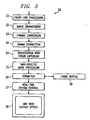
- FIGURE 3 is a block diagram of a DMD-based display system 30 having a quantizer 20 in accordance with the invention.
- a front end processing unit 31 receives input data from an external source, and performs processing such as analog to digital conversion, video decoding, deinterlacing, scaling, and on screen display generation.
- An image enhancement unit 32 performs tasks such as noise reduction, sharpness enhancement, and contrast adjustment.
- a format conversion unit 33 performs color space conversion.
- a gamma correction unit 34 performs gamma correction, resulting in the 14-bit fractional data described above as being the input to the quantization unit 20.
- Quantization unit 20 has the structure and function described above in connection with FIGURE 2.
- image processing unit 35 receives a frame of data from buffer 39 and formats in the time slice format appropriate for the DMD 38.
- a control unit 37 provides various timing and control signals to the DMD 38, which generates the images for display.
- the DMD display unit 38 includes display optics, such as a projector and related lenses, used to project the image to a screen or other image plane.
Landscapes
- Engineering & Computer Science (AREA)
- Physics & Mathematics (AREA)
- Computer Hardware Design (AREA)
- General Physics & Mathematics (AREA)
- Theoretical Computer Science (AREA)
- Control Of Indicators Other Than Cathode Ray Tubes (AREA)
- Image Processing (AREA)
- Facsimile Image Signal Circuits (AREA)
- Controls And Circuits For Display Device (AREA)
- Picture Signal Circuits (AREA)
Applications Claiming Priority (2)
| Application Number | Priority Date | Filing Date | Title |
|---|---|---|---|
| US31126501P | 2001-08-09 | 2001-08-09 | |
| US311265P | 2001-08-09 |
Publications (1)
| Publication Number | Publication Date |
|---|---|
| EP1286532A1 true EP1286532A1 (de) | 2003-02-26 |
Family
ID=23206142
Family Applications (1)
| Application Number | Title | Priority Date | Filing Date |
|---|---|---|---|
| EP02102113A Withdrawn EP1286532A1 (de) | 2001-08-09 | 2002-08-08 | Fehlerdiffusion für eine digitale Abbildungsvorrichtung |
Country Status (3)
| Country | Link |
|---|---|
| US (1) | US7076110B2 (de) |
| EP (1) | EP1286532A1 (de) |
| JP (1) | JP2003178301A (de) |
Families Citing this family (12)
| Publication number | Priority date | Publication date | Assignee | Title |
|---|---|---|---|---|
| KR100552908B1 (ko) * | 2003-12-16 | 2006-02-22 | 엘지전자 주식회사 | 플라즈마 디스플레이 패널의 구동방법 및 구동장치 |
| WO2005109387A2 (en) * | 2004-05-06 | 2005-11-17 | Thomson Licensing | Pixel shift display with minimal noise |
| MY139438A (en) * | 2004-05-06 | 2009-09-30 | Thomson Licensing Sa | Pixel shift display with minimal noise |
| MXPA05007706A (es) * | 2004-07-23 | 2006-01-26 | Thomson Licensing Sa | Metodo y dispositivo para procesamiento de datos de video al combinar difusion de error y otras oscilaciones. |
| US9299284B2 (en) * | 2004-11-10 | 2016-03-29 | Thomson Licensing | System and method for dark noise reduction in pulse width modulated (PWM) displays |
| KR100710258B1 (ko) * | 2005-06-01 | 2007-04-20 | 엘지전자 주식회사 | 디스플레이 장치의 계조 조절 장치 및 방법 |
| US7826096B2 (en) * | 2005-09-16 | 2010-11-02 | Fujifilm Corporation | Image processing method and image recording apparatus |
| GB0711462D0 (en) * | 2007-06-13 | 2007-07-25 | Digital Projection Ltd | Digital image display services |
| GB0823701D0 (en) * | 2008-12-31 | 2009-02-04 | Symbian Software Ltd | Fast data entry |
| US20130135338A1 (en) * | 2011-11-30 | 2013-05-30 | Qualcomm Mems Technologies, Inc. | Method and system for subpixel-level image multitoning |
| US10778945B1 (en) | 2019-02-28 | 2020-09-15 | Texas Instruments Incorporated | Spatial light modulator with embedded pattern generation |
| CN119948555A (zh) * | 2023-08-22 | 2025-05-06 | 京东方科技集团股份有限公司 | 显示控制方法、装置、显示设备、电子设备和存储介质 |
Citations (5)
| Publication number | Priority date | Publication date | Assignee | Title |
|---|---|---|---|---|
| EP0706165A1 (de) * | 1994-09-30 | 1996-04-10 | Texas Instruments Incorporated | Filter zur Fehlerdiffusion |
| US5686939A (en) * | 1990-11-16 | 1997-11-11 | Rank Brimar Limited | Spatial light modulators |
| US5917471A (en) * | 1995-09-28 | 1999-06-29 | Samsung Display Devices, Co., Ltd. | Method for displaying gray scales of image display unit |
| US6069609A (en) * | 1995-04-17 | 2000-05-30 | Fujitsu Limited | Image processor using both dither and error diffusion to produce halftone images with less flicker and patterns |
| US6215913B1 (en) * | 1996-01-26 | 2001-04-10 | Texas Instruments Incorporated | Non-monotonic contour diffusion and algorithm |
Family Cites Families (5)
| Publication number | Priority date | Publication date | Assignee | Title |
|---|---|---|---|---|
| US5245678A (en) * | 1991-12-20 | 1993-09-14 | Xerox Corporation | Image conversion with lossy adaptive error diffusion |
| US5479170A (en) * | 1992-10-16 | 1995-12-26 | California Institute Of Technology | Method and apparatus for long-term multi-valued storage in dynamic analog memory |
| US5377041A (en) * | 1993-10-27 | 1994-12-27 | Eastman Kodak Company | Method and apparatus employing mean preserving spatial modulation for transforming a digital color image signal |
| JP3302223B2 (ja) * | 1995-07-07 | 2002-07-15 | キヤノン株式会社 | 画像処理装置 |
| US6608700B1 (en) * | 1999-11-24 | 2003-08-19 | Xerox Corporation | Removal of error diffusion artifacts with alternating distribution weights |
-
2002
- 2002-07-17 US US10/196,918 patent/US7076110B2/en not_active Expired - Lifetime
- 2002-08-08 EP EP02102113A patent/EP1286532A1/de not_active Withdrawn
- 2002-08-09 JP JP2002233225A patent/JP2003178301A/ja active Pending
Patent Citations (5)
| Publication number | Priority date | Publication date | Assignee | Title |
|---|---|---|---|---|
| US5686939A (en) * | 1990-11-16 | 1997-11-11 | Rank Brimar Limited | Spatial light modulators |
| EP0706165A1 (de) * | 1994-09-30 | 1996-04-10 | Texas Instruments Incorporated | Filter zur Fehlerdiffusion |
| US6069609A (en) * | 1995-04-17 | 2000-05-30 | Fujitsu Limited | Image processor using both dither and error diffusion to produce halftone images with less flicker and patterns |
| US5917471A (en) * | 1995-09-28 | 1999-06-29 | Samsung Display Devices, Co., Ltd. | Method for displaying gray scales of image display unit |
| US6215913B1 (en) * | 1996-01-26 | 2001-04-10 | Texas Instruments Incorporated | Non-monotonic contour diffusion and algorithm |
Also Published As
| Publication number | Publication date |
|---|---|
| US20030031373A1 (en) | 2003-02-13 |
| US7076110B2 (en) | 2006-07-11 |
| JP2003178301A (ja) | 2003-06-27 |
Similar Documents
| Publication | Publication Date | Title |
|---|---|---|
| JP7838157B2 (ja) | 異なる表示機能の間で知覚ルミナンス非線形性ベースの画像データ交換を改善する装置および方法 | |
| EP0788087B1 (de) | Verfahren und System zu Verringerung von durch Quantisierungsfehler verursachten Artefakten in digitalen Anzeigesystemen | |
| US6965389B1 (en) | Image displaying with multi-gradation processing | |
| US6040876A (en) | Low intensity contouring and color shift reduction using dither | |
| US7076110B2 (en) | Quantization error diffusion for digital imaging devices | |
| US20080018800A1 (en) | System and method for dynamic gamma correction in digital video | |
| EP1293934B1 (de) | Farbverarbeitung-Architektur und -Algorithmen für Farblaserdrucker | |
| JPS6257139B2 (de) | ||
| CN1119808A (zh) | 增加可视显示器视在动态范围的技术 | |
| US7742190B2 (en) | Image processing method and apparatus | |
| US7126614B2 (en) | Digital, hardware based, real-time color space conversion circuitry with color saturation, brightness, contrast and hue controls | |
| US6731299B2 (en) | Apparatus and method for dithering in image processing and computer graphics systems | |
| US7265766B2 (en) | Method and system for adaptive bit depth enhancement for displays | |
| US8537076B2 (en) | Video circuit | |
| EP1575264B1 (de) | Bildverarbeitungsvorrichtung und -verfahren | |
| CN101194301B (zh) | 用于空间光调制显示系统中图像处理的设备和方法 | |
| US7791759B2 (en) | Image processing method and apparatus | |
| JP4379029B2 (ja) | 画像処理装置、画像処理方法および画像投射装置 | |
| JP3801189B2 (ja) | ビットリダクション装置 | |
| US7605832B2 (en) | Method and apparatus for improving images provided by spatial light modulated (SLM) display systems | |
| WO2002015165A1 (en) | System, method and computer program product for altering saturation in a computer graphics pipeline | |
| KR20050095779A (ko) | 스플리트 감마 테이블을 사용하는 스파클 감소 | |
| KR100546602B1 (ko) | Dlp 시스템의 기울기 향상 장치 및 방법 | |
| Ulichney | Challenges in Device-Independent Image Rendering | |
| JPH09258685A (ja) | 画像表示装置 |
Legal Events
| Date | Code | Title | Description |
|---|---|---|---|
| PUAI | Public reference made under article 153(3) epc to a published international application that has entered the european phase |
Free format text: ORIGINAL CODE: 0009012 |
|
| AK | Designated contracting states |
Kind code of ref document: A1 Designated state(s): AT BE BG CH CY CZ DE DK EE ES FI FR GB GR IE IT LI LU MC NL PT SE SK TR Designated state(s): AT BE BG CH CY CZ DE DK EE ES FI FR GB GR IE IT LI LU MC NL PT SE SK TR |
|
| AX | Request for extension of the european patent |
Extension state: AL LT LV MK RO SI |
|
| 17P | Request for examination filed |
Effective date: 20030826 |
|
| AKX | Designation fees paid |
Designated state(s): DE FR GB |
|
| 17Q | First examination report despatched |
Effective date: 20080821 |
|
| STAA | Information on the status of an ep patent application or granted ep patent |
Free format text: STATUS: THE APPLICATION IS DEEMED TO BE WITHDRAWN |
|
| 18D | Application deemed to be withdrawn |
Effective date: 20090106 |