EP1288347A2 - Verfahren zur Herstellung eines Verbindungseinkristalles - Google Patents
Verfahren zur Herstellung eines Verbindungseinkristalles Download PDFInfo
- Publication number
- EP1288347A2 EP1288347A2 EP02019020A EP02019020A EP1288347A2 EP 1288347 A2 EP1288347 A2 EP 1288347A2 EP 02019020 A EP02019020 A EP 02019020A EP 02019020 A EP02019020 A EP 02019020A EP 1288347 A2 EP1288347 A2 EP 1288347A2
- Authority
- EP
- European Patent Office
- Prior art keywords
- substrate
- compound single
- single crystalline
- undulations
- compound
- Prior art date
- Legal status (The legal status is an assumption and is not a legal conclusion. Google has not performed a legal analysis and makes no representation as to the accuracy of the status listed.)
- Withdrawn
Links
Images

Classifications
-
- C—CHEMISTRY; METALLURGY
- C30—CRYSTAL GROWTH
- C30B—SINGLE-CRYSTAL GROWTH; UNIDIRECTIONAL SOLIDIFICATION OF EUTECTIC MATERIAL OR UNIDIRECTIONAL DEMIXING OF EUTECTOID MATERIAL; REFINING BY ZONE-MELTING OF MATERIAL; PRODUCTION OF A HOMOGENEOUS POLYCRYSTALLINE MATERIAL WITH DEFINED STRUCTURE; SINGLE CRYSTALS OR HOMOGENEOUS POLYCRYSTALLINE MATERIAL WITH DEFINED STRUCTURE; AFTER-TREATMENT OF SINGLE CRYSTALS OR A HOMOGENEOUS POLYCRYSTALLINE MATERIAL WITH DEFINED STRUCTURE; APPARATUS THEREFOR
- C30B25/00—Single-crystal growth by chemical reaction of reactive gases, e.g. chemical vapour-deposition growth
- C30B25/02—Epitaxial-layer growth
- C30B25/18—Epitaxial-layer growth characterised by the substrate
-
- C—CHEMISTRY; METALLURGY
- C30—CRYSTAL GROWTH
- C30B—SINGLE-CRYSTAL GROWTH; UNIDIRECTIONAL SOLIDIFICATION OF EUTECTIC MATERIAL OR UNIDIRECTIONAL DEMIXING OF EUTECTOID MATERIAL; REFINING BY ZONE-MELTING OF MATERIAL; PRODUCTION OF A HOMOGENEOUS POLYCRYSTALLINE MATERIAL WITH DEFINED STRUCTURE; SINGLE CRYSTALS OR HOMOGENEOUS POLYCRYSTALLINE MATERIAL WITH DEFINED STRUCTURE; AFTER-TREATMENT OF SINGLE CRYSTALS OR A HOMOGENEOUS POLYCRYSTALLINE MATERIAL WITH DEFINED STRUCTURE; APPARATUS THEREFOR
- C30B25/00—Single-crystal growth by chemical reaction of reactive gases, e.g. chemical vapour-deposition growth
- C30B25/02—Epitaxial-layer growth
-
- C—CHEMISTRY; METALLURGY
- C30—CRYSTAL GROWTH
- C30B—SINGLE-CRYSTAL GROWTH; UNIDIRECTIONAL SOLIDIFICATION OF EUTECTIC MATERIAL OR UNIDIRECTIONAL DEMIXING OF EUTECTOID MATERIAL; REFINING BY ZONE-MELTING OF MATERIAL; PRODUCTION OF A HOMOGENEOUS POLYCRYSTALLINE MATERIAL WITH DEFINED STRUCTURE; SINGLE CRYSTALS OR HOMOGENEOUS POLYCRYSTALLINE MATERIAL WITH DEFINED STRUCTURE; AFTER-TREATMENT OF SINGLE CRYSTALS OR A HOMOGENEOUS POLYCRYSTALLINE MATERIAL WITH DEFINED STRUCTURE; APPARATUS THEREFOR
- C30B29/00—Single crystals or homogeneous polycrystalline material with defined structure characterised by the material or by their shape
- C30B29/10—Inorganic compounds or compositions
- C30B29/36—Carbides
Definitions
- the present invention relates to a method of manufacturing compound single crystals that are useful as electronic materials.
- the present invention relates to a method of manufacturing compound single crystals that are desirable from the aspect of improving the yield and characteristics of semiconductor devices during the manufacturing thereof, that have a low defect density, and that present little crystal lattice deformation.
- substrates employed in semiconductor devices have been cut into platelike ingots of compound semiconductor crystal, for example, processed into specific external shapes, surface ground, and employed as semiconductor wafers. Further, in the course of manufacturing high-performance semiconductor devices, films with few crystal defects and low impurity concentrations have been epitaxially grown on compound semiconductor substrates obtained by processing these ingots.
- planar defects are generated in the SiC film.
- a method of reducing these planar defects has been proposed that consists of the steps of providing growth regions on a growth substrate and growing silicon carbide single crystal on these growth regions to a thickness greater than or equal to the natural thickness of the substrate in the orientation of the growth plane (Japanese Examined Patent Publication (KOKOKU) Hei 6-41400).
- the two antiphase regions contained in the SiC are characterized by expanding in mutually perpendicular orientations as the SiC increases in film thickness. Thus, it has not been possible to effectively reduce antiphase boundaries even with continued heteroepitaxial growth.
- One means of eliminating crystal lattice nonconformity is to insert another layer (buffer layer) having a lattice constant falling between that of the substrate and the layer grown over it.
- buffer layer having a lattice constant falling between that of the substrate and the layer grown over it.
- lattice constant nonconformity 20 percent results when directly growing SiC on a Si substrate, becoming the principal cause of planar defects in the epitaxially grown layer of SiC.
- K. Shibahara et al. have proposed a method of growth on a silicon (001) surface substrate in which the surface normal axis is slightly tilted (in which an off angle is introduced) from the ⁇ 001> direction in the ⁇ 110> direction as a method of effectively reducing antiphase boundaries (Applied Physics Letter, Vol. 50, 1987, p. 1,888).
- antiphase boundaries generated at silicon substrate surface terraces are eliminated at the points where antiphase boundaries meet, but antiphase boundaries generated at single atom steps in the silicon substrate do not meet one another and are not eliminated.
- planar defects twins, APBs
- the present inventors have proposed the technique of eliminating planar defects propagating within silicon carbide by imparting undulations extending in a direction parallel to the silicon substrate surface and epitaxially growing silicon carbide on a substrate that has been processed with such undulations (Japanese Patent Application (TOKUGAN) No. 2000-365443 and Japanese Unexamined Patent Publication (KOKAI) No. 2000-178740).
- This method yields silicon carbide in which planar defects are greatly reduced.
- gallium nitride is expected to serve as blue LEDs and power device materials.
- gallium nitride has been numerous reports and examples of the growth of gallium nitride on silicon carbide substrates in recent years. This is because the use of silicon carbide as a base substrate in the growth of gallium nitride affords such advantages as facilitating the formation of electrodes, permitting ready heat dissipation, and facilitating handling and processing due to an identical crystal cleavage direction.
- GaN gallium nitride
- the present invention intends to overcome at least some of the above problems.
- the object is solved by the method according to independent claim 1. Further advantages, features, aspects and details of the invention are evident from the dependent claims, the description and the accompanying drawings.
- the present invention generally relates to a method of manufacturing compound single crystals which are e.g. useful as electronic material.
- One object of the present invention is e.g. to provide a method of manufacturing compound single crystals by epitaxially growing a compound single crystal layer differing from the substrate in which the planar defects generated in the crystal that is epitaxially grown are reduced.
- a compound single crystalline layer differing from a compound single crystalline substrate is epitaxially grown on the surface of the substrate.
- This manufacturing method is characterized in that plural undulations extending in a single direction are present on at least a portion of the surface of said substrate, and in that said undulations are provided in such a manner that as said compound single crystalline layer epitaxially grows, the defects that grow meet each other.
- the compound constituting the compound single crystalline substrate employed in the manufacturing method of the present invention may be, for example, a group IV-IV compound, group III-V compound, or group II-VI compound.
- Specific examples are compounds (semiconductors) such as SiC, GaAs, AlAs, InAs, GaP, GaSb, InP, InSb, ZnS, ZnSe, CdS, CdTe, and HgTe.
- Sapphire is an example of a compound constituting the compound single crystalline substrate.
- the compound constituting the compound single crystalline substrate may be a crystal of any space lattice, examples of which are cubic and hexagonal structures. More specific examples of the single crystalline substrate are cubic SiC substrates having a (001) basal plane and hexagonal SiC substrates having a (11-20) or (1100) basal plane.
- the compound single crystal that is epitaxially grown by the manufacturing method of the present invention may be suitably selected from among the compounds given above as examples of compounds constituting the compound single crystalline substrate. More specific examples of the compound single crystalline layers are gallium nitride, aluminum nitride, indium gallium nitride, and aluminum gallium nitride.
- the method of manufacturing compound single crystals of the present invention in which a compound single crystalline layer differing from a compound single crystalline substrate is epitaxially grown, is particularly effective when the compound single crystal constituting the compound single crystalline layer and the compound single crystal constituting the compound single crystalline substrate have similar space lattices.
- the statement that the two single crystals have similar space lattices means that the positional relations between the atoms of the structural units of the crystals (base unit structures) are similar, the bonding orientation between atoms is identical, and they grow in the same crystal axis orientation (epitaxial growth).
- examples of two single crystals having similar space lattices are cubic GaN/cubic SiC, hexagonal GaN/hexagonal SiC, hexagonal AlN/hexagonal SiC, hexagonal AlGaN/hexagonal SiC, cubic AlN/cubic SiC, and hexagonal (4H) SiC/hexagonal (6H) SiC.
- the substrate employed in the manufacturing method of the present invention comprises plural undulations extending in a single direction on at least part of the surface thereof.
- Plural undulations are provided on at least a portion of the substrate surface, but are desirably provided on the entire surface on which epitaxial growth is conducted. Further, the undulations are provided in such a manner that defects growing with epitaxial growth of the compound single crystalline layer meet each other. More specifically, the plural undulations have wavy or serrated cross-sectional shapes perpendicular to the direction of extension of the undulations.
- Fig. 1 shows an example of plural undulations having a wavy cross-section.
- the wavy shape of the undulations will be described in greater detail.
- the cross-sectional shape of the plural undulations provided on the substrate surface is wavy.
- all of the waves extend in a single direction.
- the inclined surfaces of adjacent undulation peaks are opposed, and this state is continuous.
- the distance from peak to peak of the undulations is referred to as the period, and the difference in height between peaks and valleys is referred to as the amplitude (see Fig. 2).
- the angle formed by the inclined surface running from peak to valley relative to the average line of the substrate surface is referred to as the gradient of slope.
- the length of the period ranges from about 0.01 micrometer to 1 mm, preferably from 0.1 micrometer to 10 micrometers.
- the magnitude of amplitude is from 1 nm to 50 micrometers, preferably from 10 to 100 nm.
- the gradient of slope is from 0.1° to 54.7° (for example, an angle smaller than the angle formed by the (001) face and the (111) face), preferably from 1 to 6°.
- the undulations may extend in any direction to achieve the effect of eliminating planar defects, but desirably extend in a direction parallel to the ⁇ 110> orientation to effectively eliminate planer defects of ⁇ 111 ⁇ faces.
- the gradient of slope may be an angle (the angle varies with the crystal lattice constant) smaller than the angle formed by ⁇ 1-101 ⁇ relative to the (0001) growth face, for example.
- the surface having undulations may be obtained by processing by grinding (grinding in which rubbing is limited to a single direction), for example. Although some variation in the individual shape of undulations results from variation in the type and striking method of the grinding wheel or abrasive, conditions can be optimized to achieve undulations with shapes roughly corresponding to those set forth above.
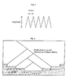
- serrated undulations In contrast to wavy undulations, serrated undulations have sharply angled peaks and valleys (see Fig. 3).
- the distance from undulation peak to peak is referred to as the period and the difference in height between peaks and valleys is referred to as the amplitude.
- the angle formed by the inclined surface running from peak to valley relative to the average line of the substrate surface is referred to as the gradient of slope.
- the length of the period ranges from about 0.01 micrometer to 1 mm, preferably from 0.1 micrometer to 10 micrometers.
- the magnitude of amplitude is from 1 nm to 50 micrometers, preferably from 10 to 100 nm.
- the gradient of slope is from 0.1° to 54.7° (for example, an angle smaller than the angle formed by the (001) face and the (111) face), preferably from 1 to 6°.
- the undulations may extend in any direction to achieve the effect of eliminating planar defects, but desirably extend in a direction parallel to the ⁇ 110> orientation to effectively eliminate planer defects of ⁇ 111 ⁇ faces.
- the individual undulations are formed so that inclined surfaces having gradients smaller than 90° with the basal plane are opposed, and are desirably shaped so that when the inclination of the surface relative to the basal plane is integrated over the entire surface, the value obtained is essentially 0°.
- Compound single crystalline substrates with the above-mentioned undulations having wavy or serrated cross-sections perpendicular to the direction in which the undulations extend may be produced, for example, by photolithographic techniques, press processing techniques, laser processing and ultrasound processing techniques, and processing by grinding. No matter which method is employed, it suffices for the final form of the growth substrate surface and single crystalline layer to permit defects growing during epitaxial growth to meet.
- the line width of the pattern can be changed to control the width of the undulation shape.
- the selected etching rates of the resist and the substrate can be controlled to regulate the depth of the undulation pattern and angle of the inclined surface.
- the press mold can be shaped to yield any desired shape of undulation on the growth substrate. Molds of various shape can be formed to form various shapes of undulation on the growth substrate.
- the undulation shape is directly formed on the substrate.
- the abrasive particle size employed in grinding and the processing pressure can be varied to control the width and depth of the undulation shape.
- the etching conditions and shape of the etching mask can be changed to control the width and depth of the undulation shape.
- the etching mask can be positioned away from the substrate on which patterns are transferred to transfer wavy or serrated patterns due to the etching being diffused between the mask and the substrate.
- a mask having a window cross-section of pedestal shape widening toward the substrate on which patterns are transferred may also be employed.
- a compound single crystal is epitaxially grown on the surface of the above-described substrate.
- Methods of epitaxially growing compound single crystals that are suitable for use include chemical vapor deposition (CVD), liquid phase epitaxy, sputtering, and molecular beam epitaxy (MBE). More specifically, a Ga source (for example, trimethylgallium) and a N source (for example, ammonia) are simultaneously fed and GaN is grown on a substrate in the form of the substrate set forth above using a MOCVD equipment. When growing AlGaN, an Al source (for example, trimethylaluminum) is further supplied. Providing undulations on the substrate makes it possible to position off-inclined surfaces opposite each other on the substrate as shown in Fig. 4 so that opposing planar defects meet each other and are eliminated.
- Undulations were imparted to 3C-SiC and gallium nitride (GaN) was formed thereon.
- the processing of undulations on the 3C-SiC surface was conducted in the following manner. Diamond compound 60 micrometers in diameter was coated on M414 cloth made by Engis Co. and SiC was rubbed in a single direction over the cloth. The pressure applied in this process was 0.1 kg/cm 2 .
- the undulation-processed substrate obtained was treated by thermal oxidation (1,100°C, 5 hours, O 2 atmosphere) and the oxide film was removed with diluted HF.
- Trimethylgallium and ammonia were supplied with an organic metal chemical vapor deposition (MOCVD) equipment to the 3C-SiC substrate surface obtained to form GaN.
- the growth temperature was 1,100°C, 20 slm of nitrogen as carrier gas, 10 slm of ammonia (NH 3 ) and 1 x 10 -4 mol/min of trimethylgallium were fed.
- the film thickness was about 10 micrometers.
- the twin density in the resultant GaN was obtained from an X-ray diffraction peak pole figure in the manner set forth below.
- a GaN (111) face diffraction pole figure was prepared with the GaN (001) face as pole and the twin density was calculated from the ratio of the signal intensity in the orientation of ⁇ 115 ⁇ faces corresponding to twin planes to the signal intensity in the orientation of ⁇ 111 ⁇ faces of a normal single crystalline surface.
- the result revealed the twin density to be less than or equal to the measurement limit of 4 x 10 -4 Vol.%.
- GaN was formed on 3C-SiC that had not been undulation processed. The same method of formation was employed as in Example 1.
- the twin density of the GaN obtained was calculated in the following manner.
- a GaN (111) face diffraction pole figure was prepared with the GaN (001) face as pole and the twin density was calculated from the ratio of the signal intensity in the orientation of ⁇ 115 ⁇ faces corresponding to twin planes to the signal intensity in the orientation of ⁇ 111 ⁇ faces of a normal single crystalline surface.
- the surface of a 3C-SiC substrate 200 micrometers in thickness obtained by CVD was processed to impart undulation.
- Abrasive was rubbed in parallel to the ⁇ 110> direction on the surface of a SiC (001) substrate six inches in diameter to prepare a substrate having undulations parallel to the ⁇ 110> direction.
- the abrasives employed were commercially available about 15 micrometer diameter diamond slurry (Hipress made by Engis Co.) and commercially available abrasive cloth (Engis M414).
- the cloth was impregnated with diamond slurry uniformly, the Si (001) substrate was placed on the pad, a pressure of 0.2 kg/cm 2 was applied over the entire SiC (001) substrate, and [the substrate] was run about 300 times back and forth over the cloth over a distance of about 20 cm parallel to the ⁇ 110> direction (single direction grinding processing).
- Countless abrasive striations (undulations) were formed on the SiC (001) substrate surface parallel to the ⁇ 110> direction.
- a thermal oxidation film of about 0.1 micrometer was formed and the oxide film was then removed to etch the substrate surface by about 200 Angstroms, removing the minute irregularities and yielding extremely smooth undulations.
- a look at the wavy cross-section revealed the wavy irregularities to be irregular and unstable in size, but high in density. They were always in a continuously undulating state.
- the depth of the channels was 30 to 50 nm and the width thereof was 1 to 2 micrometers.
- the gradient of slope was 3 to 5°.
- Equipment Atmospheric pressure heat treatment furnace Temperature 1,000 to 1,200°C Oxygen flow rate 1 to 5 slm (100 to 1,000 sccm steam) Diluting gas (argon) flow rate 1 to 5 slm Processing time 3 hours
- Aluminum nitride (AlN) was formed on the above 3C-SiC.
- An organic metal chemical vapor deposition (MOCVD) equipment was employed to feed trimethylaluminum and ammonia, and AlN was formed.
- the growth temperature was 1,100°C, 20 slm of nitrogen as carrier gas, 10 slm of ammonia (NH 3 ) and 1 x 10 -4 mol/min of trimethylaluminum were fed.
- the film thickness was made about 10 micrometers.
- the twin density of the AlN was obtained as follows. An AlN (111) face diffraction pole figure with the AlN (001) face as pole was prepared and the twin density was calculated from the ratio of the signal intensity in the orientation of ⁇ 115 ⁇ faces corresponding to twin planes to the signal intensity in the orientation of ⁇ 111 ⁇ faces of a normal single crystalline surface. The results revealed the twin density to be less than or equal to the measurement limit of 4 x 10 -4 Vol.%.
- AlN was formed on 3C-SiC that had not been undulation processed as a comparative example.
- the method of formation was identical to that employed in Example 2.
- the twin density of the AlN obtained was obtained in the following manner. An AlN (111) face diffraction pole figure with the AlN (001) face as pole was prepared and the twin density was calculated from the ratio of the signal intensity in the orientation of ⁇ 115 ⁇ faces corresponding to twin planes to the signal intensity in the orientation of ⁇ 111 ⁇ faces of a normal single crystalline surface. The results revealed the twin density to be 7 x 10 -3 Vol.%.
- the present invention provides a method of manufacturing compound single crystals by epitaxially growing a compound single crystalline layer differing from the substrate, permitting a reduction in the planar defects generated within crystal that is epitaxially grown.
Landscapes
- Chemical & Material Sciences (AREA)
- Metallurgy (AREA)
- Engineering & Computer Science (AREA)
- Crystallography & Structural Chemistry (AREA)
- Materials Engineering (AREA)
- Organic Chemistry (AREA)
- General Chemical & Material Sciences (AREA)
- Chemical Kinetics & Catalysis (AREA)
- Inorganic Chemistry (AREA)
- Crystals, And After-Treatments Of Crystals (AREA)
- Recrystallisation Techniques (AREA)
- Led Devices (AREA)
- Chemical Vapour Deposition (AREA)
Applications Claiming Priority (2)
| Application Number | Priority Date | Filing Date | Title |
|---|---|---|---|
| JP2001256295 | 2001-08-27 | ||
| JP2001256295A JP2003068655A (ja) | 2001-08-27 | 2001-08-27 | 化合物単結晶の製造方法 |
Publications (2)
| Publication Number | Publication Date |
|---|---|
| EP1288347A2 true EP1288347A2 (de) | 2003-03-05 |
| EP1288347A3 EP1288347A3 (de) | 2006-08-23 |
Family
ID=19084125
Family Applications (1)
| Application Number | Title | Priority Date | Filing Date |
|---|---|---|---|
| EP02019020A Withdrawn EP1288347A3 (de) | 2001-08-27 | 2002-08-26 | Verfahren zur Herstellung eines Verbindungseinkristalles |
Country Status (4)
| Country | Link |
|---|---|
| US (1) | US7101774B2 (de) |
| EP (1) | EP1288347A3 (de) |
| JP (1) | JP2003068655A (de) |
| KR (1) | KR20030019151A (de) |
Cited By (1)
| Publication number | Priority date | Publication date | Assignee | Title |
|---|---|---|---|---|
| EP1889953A4 (de) * | 2005-06-07 | 2014-03-19 | Hoya Corp | Herstellungsverfahren für einen siliciumcarbid-einzelkristall |
Families Citing this family (11)
| Publication number | Priority date | Publication date | Assignee | Title |
|---|---|---|---|---|
| WO2004086472A1 (en) * | 2003-03-28 | 2004-10-07 | Koninklijke Philips Electronics N.V. | Method of epitaxial deposition of an n-doped silicon layer |
| KR100714639B1 (ko) | 2003-10-21 | 2007-05-07 | 삼성전기주식회사 | 발광 소자 |
| TWI408263B (zh) * | 2004-07-01 | 2013-09-11 | 住友電氣工業股份有限公司 | AlxGayIn1-x-yN基板、AlxGayIn1-x-yN基板之清潔方法、AlN基板及AlN基板之清潔方法 |
| KR100593936B1 (ko) | 2005-03-25 | 2006-06-30 | 삼성전기주식회사 | 비극성 a면 질화갈륨 단결정 제조방법 |
| ITMI20070056A1 (it) | 2007-01-17 | 2008-07-18 | Consiglio Nazionale Ricerche | Substrato semiconduttore adatto alla realizzazione di dispositivi elettronici e-o optoelettronici e relativo processo di fabbricazione |
| US8890103B2 (en) | 2007-01-17 | 2014-11-18 | Consiglio Nazionale Delle Ricerche | Semiconductor substrate suitable for the realisation of electronic and/or optoelectronic devices and relative manufacturing process |
| JP4462289B2 (ja) * | 2007-05-18 | 2010-05-12 | ソニー株式会社 | 半導体層の成長方法および半導体発光素子の製造方法 |
| JP5345499B2 (ja) * | 2009-10-15 | 2013-11-20 | Hoya株式会社 | 化合物単結晶およびその製造方法 |
| US9275861B2 (en) | 2013-06-26 | 2016-03-01 | Globalfoundries Inc. | Methods of forming group III-V semiconductor materials on group IV substrates and the resulting substrate structures |
| JP6953843B2 (ja) * | 2017-07-07 | 2021-10-27 | セイコーエプソン株式会社 | 単結晶基板および炭化ケイ素基板 |
| JP6795805B1 (ja) | 2020-05-15 | 2020-12-02 | 株式会社Cusic | SiC積層体およびその製造方法ならびに半導体装置 |
Family Cites Families (21)
| Publication number | Priority date | Publication date | Assignee | Title |
|---|---|---|---|---|
| US5294370A (en) * | 1988-11-15 | 1994-03-15 | Hbt Holland Biotechnology B.V. | Selenium or tellurium elemental hydrosols and their preparation |
| US4946547A (en) * | 1989-10-13 | 1990-08-07 | Cree Research, Inc. | Method of preparing silicon carbide surfaces for crystal growth |
| AU8877991A (en) * | 1990-10-09 | 1992-04-28 | Harold R. Pilley | Airport control/management system |
| JP2556621B2 (ja) * | 1990-12-11 | 1996-11-20 | ホーヤ株式会社 | 炭化ケイ素膜の成膜方法 |
| JPH051380A (ja) * | 1991-06-24 | 1993-01-08 | Hoya Corp | 炭化ケイ素の成膜方法 |
| EP0874405A3 (de) * | 1997-03-25 | 2004-09-15 | Mitsubishi Cable Industries, Ltd. | Element auf Basis von GaN mit niedriger Versetzungsdichte, seine Verwendung und Herstellungsverfahren |
| US5915194A (en) * | 1997-07-03 | 1999-06-22 | The United States Of America As Represented By The Administrator Of National Aeronautics And Space Administration | Method for growth of crystal surfaces and growth of heteroepitaxial single crystal films thereon |
| US6051849A (en) * | 1998-02-27 | 2000-04-18 | North Carolina State University | Gallium nitride semiconductor structures including a lateral gallium nitride layer that extends from an underlying gallium nitride layer |
| US6294440B1 (en) * | 1998-04-10 | 2001-09-25 | Sharp Kabushiki Kaisha | Semiconductor substrate, light-emitting device, and method for producing the same |
| US6265289B1 (en) * | 1998-06-10 | 2001-07-24 | North Carolina State University | Methods of fabricating gallium nitride semiconductor layers by lateral growth from sidewalls into trenches, and gallium nitride semiconductor structures fabricated thereby |
| JP3201475B2 (ja) * | 1998-09-14 | 2001-08-20 | 松下電器産業株式会社 | 半導体装置およびその製造方法 |
| US6252261B1 (en) * | 1998-09-30 | 2001-06-26 | Nec Corporation | GaN crystal film, a group III element nitride semiconductor wafer and a manufacturing process therefor |
| JP3576432B2 (ja) * | 1998-10-10 | 2004-10-13 | Hoya株式会社 | 炭化珪素膜及びその製造方法 |
| EP1130135B1 (de) * | 1999-10-08 | 2007-08-08 | Hoya Corporation | Siliziumkarbidschicht und Herstellungsverfahren |
| JP3550070B2 (ja) * | 1999-03-23 | 2004-08-04 | 三菱電線工業株式会社 | GaN系化合物半導体結晶、その成長方法及び半導体基材 |
| US6596080B2 (en) * | 2000-04-07 | 2003-07-22 | Hoya Corporation | Silicon carbide and method for producing the same |
| JP3707726B2 (ja) * | 2000-05-31 | 2005-10-19 | Hoya株式会社 | 炭化珪素の製造方法、複合材料の製造方法 |
| JP3650727B2 (ja) * | 2000-08-10 | 2005-05-25 | Hoya株式会社 | 炭化珪素製造方法 |
| JP2002220299A (ja) * | 2001-01-19 | 2002-08-09 | Hoya Corp | 単結晶SiC及びその製造方法、SiC半導体装置並びにSiC複合材料 |
| KR100425343B1 (ko) * | 2001-04-17 | 2004-03-30 | 삼성전기주식회사 | 반도체 기판 제조방법 |
| JP2003068654A (ja) * | 2001-08-27 | 2003-03-07 | Hoya Corp | 化合物単結晶の製造方法 |
-
2001
- 2001-08-27 JP JP2001256295A patent/JP2003068655A/ja active Pending
-
2002
- 2002-08-26 EP EP02019020A patent/EP1288347A3/de not_active Withdrawn
- 2002-08-26 US US10/227,336 patent/US7101774B2/en not_active Expired - Fee Related
- 2002-08-27 KR KR1020020050931A patent/KR20030019151A/ko not_active Withdrawn
Cited By (1)
| Publication number | Priority date | Publication date | Assignee | Title |
|---|---|---|---|---|
| EP1889953A4 (de) * | 2005-06-07 | 2014-03-19 | Hoya Corp | Herstellungsverfahren für einen siliciumcarbid-einzelkristall |
Also Published As
| Publication number | Publication date |
|---|---|
| KR20030019151A (ko) | 2003-03-06 |
| US20030045102A1 (en) | 2003-03-06 |
| JP2003068655A (ja) | 2003-03-07 |
| US7101774B2 (en) | 2006-09-05 |
| EP1288347A3 (de) | 2006-08-23 |
Similar Documents
| Publication | Publication Date | Title |
|---|---|---|
| US6736894B2 (en) | Method of manufacturing compound single crystal | |
| EP1258544B1 (de) | Kristall einer Verbindung und Verfahren zur deren Herstellung | |
| US5363800A (en) | Process for the controlled growth of single-crystal films of silicon carbide polytypes on silicon carbide wafers | |
| EP1143033B1 (de) | Siliciumkarbid und Verfahren zu seiner Herstellung | |
| CN100424817C (zh) | 半导体用氮化物衬底的制备方法及氮化物半导体衬底 | |
| JP4691911B2 (ja) | Iii−v族窒化物系半導体自立基板の製造方法 | |
| Yasutoshi Kawaguchi et al. | Selective area growth of GaN on Si substrate using SiO 2 mask by metalorganic vapor phase epitaxy | |
| US7101774B2 (en) | Method of manufacturing compound single crystal | |
| US6461944B2 (en) | Methods for growth of relatively large step-free SiC crystal surfaces | |
| JP2002255694A (ja) | 半導体用基板とその製造方法 | |
| EP2312023A2 (de) | Verbindungseinkristall und Herstellungsverfahren dafür | |
| EP2093312A1 (de) | Verfahren zur Herstellung von Gruppe-III-Nidridkristall | |
| EP1889953A1 (de) | Herstellungsverfahren für einen siliciumcarbid-einzelkristall | |
| Saddow et al. | Lateral Epitaxial Overgrowth and pendeo epitaxy of 3C-SiC on Si substrates | |
| Marchand et al. | Extended defect reduction in GaN laterally overgrown on Si (lll) | |
| JP2004336079A (ja) | 化合物単結晶の製造方法 | |
| JP3581145B6 (ja) | 窒化物半導体基板の加工方法 | |
| Nishino et al. | Channel Epitaxy of 3C-SiC on Si Substrates by CVD |
Legal Events
| Date | Code | Title | Description |
|---|---|---|---|
| PUAI | Public reference made under article 153(3) epc to a published international application that has entered the european phase |
Free format text: ORIGINAL CODE: 0009012 |
|
| AK | Designated contracting states |
Kind code of ref document: A2 Designated state(s): AT BE BG CH CY CZ DE DK EE ES FI FR GB GR IE IT LI LU MC NL PT SE SK TR Designated state(s): AT BE BG CH CY CZ DE DK EE ES FI FR GB GR IE IT LI LU MC NL PT SE SK TR |
|
| AX | Request for extension of the european patent |
Extension state: AL LT LV MK RO SI |
|
| PUAL | Search report despatched |
Free format text: ORIGINAL CODE: 0009013 |
|
| AK | Designated contracting states |
Kind code of ref document: A3 Designated state(s): AT BE BG CH CY CZ DE DK EE ES FI FR GB GR IE IT LI LU MC NL PT SE SK TR |
|
| AX | Request for extension of the european patent |
Extension state: AL LT LV MK RO SI |
|
| 17P | Request for examination filed |
Effective date: 20070219 |
|
| AKX | Designation fees paid |
Designated state(s): AT BE BG CH CY CZ DE DK EE ES FI FR GB GR IE IT LI LU MC NL PT SE SK TR |
|
| 17Q | First examination report despatched |
Effective date: 20060529 |
|
| STAA | Information on the status of an ep patent application or granted ep patent |
Free format text: STATUS: THE APPLICATION IS DEEMED TO BE WITHDRAWN |
|
| 18D | Application deemed to be withdrawn |
Effective date: 20071009 |