EP1288977A1 - Elements de dispositifs de systèmes mécaniques microélectriques avec résistance à couches minces couplé à une électrode de contact - Google Patents
Elements de dispositifs de systèmes mécaniques microélectriques avec résistance à couches minces couplé à une électrode de contact Download PDFInfo
- Publication number
- EP1288977A1 EP1288977A1 EP02102230A EP02102230A EP1288977A1 EP 1288977 A1 EP1288977 A1 EP 1288977A1 EP 02102230 A EP02102230 A EP 02102230A EP 02102230 A EP02102230 A EP 02102230A EP 1288977 A1 EP1288977 A1 EP 1288977A1
- Authority
- EP
- European Patent Office
- Prior art keywords
- resistor
- bottom electrode
- etching
- hard mask
- switch
- Prior art date
- Legal status (The legal status is an assumption and is not a legal conclusion. Google has not performed a legal analysis and makes no representation as to the accuracy of the status listed.)
- Granted
Links
- 230000015572 biosynthetic process Effects 0.000 title description 6
- 239000000463 material Substances 0.000 claims abstract description 37
- 238000000034 method Methods 0.000 claims abstract description 28
- 239000007769 metal material Substances 0.000 claims abstract description 19
- 239000000758 substrate Substances 0.000 claims abstract description 19
- 238000000151 deposition Methods 0.000 claims abstract description 18
- 238000005530 etching Methods 0.000 claims abstract description 16
- VYPSYNLAJGMNEJ-UHFFFAOYSA-N Silicium dioxide Chemical compound O=[Si]=O VYPSYNLAJGMNEJ-UHFFFAOYSA-N 0.000 claims description 14
- VNNRSPGTAMTISX-UHFFFAOYSA-N chromium nickel Chemical compound [Cr].[Ni] VNNRSPGTAMTISX-UHFFFAOYSA-N 0.000 claims description 9
- 229910001120 nichrome Inorganic materials 0.000 claims description 9
- 239000000377 silicon dioxide Substances 0.000 claims description 7
- 229910018125 Al-Si Inorganic materials 0.000 claims description 5
- 229910018520 Al—Si Inorganic materials 0.000 claims description 5
- 229910052681 coesite Inorganic materials 0.000 claims description 4
- 229910052906 cristobalite Inorganic materials 0.000 claims description 4
- 229910052682 stishovite Inorganic materials 0.000 claims description 4
- 229910052905 tridymite Inorganic materials 0.000 claims description 4
- 235000012239 silicon dioxide Nutrition 0.000 claims description 3
- 238000000059 patterning Methods 0.000 claims 4
- 238000001039 wet etching Methods 0.000 claims 2
- XUIMIQQOPSSXEZ-UHFFFAOYSA-N Silicon Chemical compound [Si] XUIMIQQOPSSXEZ-UHFFFAOYSA-N 0.000 abstract description 12
- 229910052710 silicon Inorganic materials 0.000 abstract description 12
- 239000010703 silicon Substances 0.000 abstract description 12
- 230000008569 process Effects 0.000 abstract description 4
- 238000004519 manufacturing process Methods 0.000 description 13
- 239000012528 membrane Substances 0.000 description 12
- 239000003990 capacitor Substances 0.000 description 9
- 239000010409 thin film Substances 0.000 description 8
- 239000002184 metal Substances 0.000 description 7
- 229910052751 metal Inorganic materials 0.000 description 7
- 229910008599 TiW Inorganic materials 0.000 description 6
- 238000005516 engineering process Methods 0.000 description 4
- 241000208967 Polygala cruciata Species 0.000 description 3
- 230000008021 deposition Effects 0.000 description 3
- -1 photo-resist Substances 0.000 description 3
- 238000004891 communication Methods 0.000 description 2
- 238000013461 design Methods 0.000 description 2
- 238000003780 insertion Methods 0.000 description 2
- 230000037431 insertion Effects 0.000 description 2
- 239000012212 insulator Substances 0.000 description 2
- 229910021420 polycrystalline silicon Inorganic materials 0.000 description 2
- 229920005591 polysilicon Polymers 0.000 description 2
- 125000006850 spacer group Chemical group 0.000 description 2
- JBRZTFJDHDCESZ-UHFFFAOYSA-N AsGa Chemical compound [As]#[Ga] JBRZTFJDHDCESZ-UHFFFAOYSA-N 0.000 description 1
- 229910001218 Gallium arsenide Inorganic materials 0.000 description 1
- 229910052581 Si3N4 Inorganic materials 0.000 description 1
- 229910052782 aluminium Inorganic materials 0.000 description 1
- XAGFODPZIPBFFR-UHFFFAOYSA-N aluminium Chemical compound [Al] XAGFODPZIPBFFR-UHFFFAOYSA-N 0.000 description 1
- PNEYBMLMFCGWSK-UHFFFAOYSA-N aluminium oxide Inorganic materials [O-2].[O-2].[O-2].[Al+3].[Al+3] PNEYBMLMFCGWSK-UHFFFAOYSA-N 0.000 description 1
- 238000003491 array Methods 0.000 description 1
- 230000005540 biological transmission Effects 0.000 description 1
- 239000000969 carrier Substances 0.000 description 1
- 230000015556 catabolic process Effects 0.000 description 1
- 239000004020 conductor Substances 0.000 description 1
- 230000008878 coupling Effects 0.000 description 1
- 238000010168 coupling process Methods 0.000 description 1
- 238000005859 coupling reaction Methods 0.000 description 1
- 230000005686 electrostatic field Effects 0.000 description 1
- 239000011521 glass Substances 0.000 description 1
- 238000002513 implantation Methods 0.000 description 1
- 230000010354 integration Effects 0.000 description 1
- 238000002955 isolation Methods 0.000 description 1
- 150000002739 metals Chemical class 0.000 description 1
- 238000005459 micromachining Methods 0.000 description 1
- 238000012986 modification Methods 0.000 description 1
- 230000004048 modification Effects 0.000 description 1
- 229920003229 poly(methyl methacrylate) Polymers 0.000 description 1
- 239000004926 polymethyl methacrylate Substances 0.000 description 1
- 238000012545 processing Methods 0.000 description 1
- 230000008707 rearrangement Effects 0.000 description 1
- 229910052594 sapphire Inorganic materials 0.000 description 1
- 239000010980 sapphire Substances 0.000 description 1
- 239000004065 semiconductor Substances 0.000 description 1
- 239000007787 solid Substances 0.000 description 1
- 230000003068 static effect Effects 0.000 description 1
- 238000006467 substitution reaction Methods 0.000 description 1
- PBCFLUZVCVVTBY-UHFFFAOYSA-N tantalum pentoxide Inorganic materials O=[Ta](=O)O[Ta](=O)=O PBCFLUZVCVVTBY-UHFFFAOYSA-N 0.000 description 1
- 238000012546 transfer Methods 0.000 description 1
Images



Classifications
-
- H—ELECTRICITY
- H01—ELECTRIC ELEMENTS
- H01H—ELECTRIC SWITCHES; RELAYS; SELECTORS; EMERGENCY PROTECTIVE DEVICES
- H01H59/00—Electrostatic relays; Electro-adhesion relays
- H01H59/0009—Electrostatic relays; Electro-adhesion relays making use of micromechanics
-
- H—ELECTRICITY
- H01—ELECTRIC ELEMENTS
- H01H—ELECTRIC SWITCHES; RELAYS; SELECTORS; EMERGENCY PROTECTIVE DEVICES
- H01H1/00—Contacts
- H01H1/0036—Switches making use of microelectromechanical systems [MEMS]
-
- Y—GENERAL TAGGING OF NEW TECHNOLOGICAL DEVELOPMENTS; GENERAL TAGGING OF CROSS-SECTIONAL TECHNOLOGIES SPANNING OVER SEVERAL SECTIONS OF THE IPC; TECHNICAL SUBJECTS COVERED BY FORMER USPC CROSS-REFERENCE ART COLLECTIONS [XRACs] AND DIGESTS
- Y10—TECHNICAL SUBJECTS COVERED BY FORMER USPC
- Y10T—TECHNICAL SUBJECTS COVERED BY FORMER US CLASSIFICATION
- Y10T29/00—Metal working
- Y10T29/43—Electric condenser making
- Y10T29/435—Solid dielectric type
-
- Y—GENERAL TAGGING OF NEW TECHNOLOGICAL DEVELOPMENTS; GENERAL TAGGING OF CROSS-SECTIONAL TECHNOLOGIES SPANNING OVER SEVERAL SECTIONS OF THE IPC; TECHNICAL SUBJECTS COVERED BY FORMER USPC CROSS-REFERENCE ART COLLECTIONS [XRACs] AND DIGESTS
- Y10—TECHNICAL SUBJECTS COVERED BY FORMER USPC
- Y10T—TECHNICAL SUBJECTS COVERED BY FORMER US CLASSIFICATION
- Y10T29/00—Metal working
- Y10T29/49—Method of mechanical manufacture
- Y10T29/49002—Electrical device making
- Y10T29/49004—Electrical device making including measuring or testing of device or component part
-
- Y—GENERAL TAGGING OF NEW TECHNOLOGICAL DEVELOPMENTS; GENERAL TAGGING OF CROSS-SECTIONAL TECHNOLOGIES SPANNING OVER SEVERAL SECTIONS OF THE IPC; TECHNICAL SUBJECTS COVERED BY FORMER USPC CROSS-REFERENCE ART COLLECTIONS [XRACs] AND DIGESTS
- Y10—TECHNICAL SUBJECTS COVERED BY FORMER USPC
- Y10T—TECHNICAL SUBJECTS COVERED BY FORMER US CLASSIFICATION
- Y10T29/00—Metal working
- Y10T29/49—Method of mechanical manufacture
- Y10T29/49002—Electrical device making
- Y10T29/4902—Electromagnet, transformer or inductor
-
- Y—GENERAL TAGGING OF NEW TECHNOLOGICAL DEVELOPMENTS; GENERAL TAGGING OF CROSS-SECTIONAL TECHNOLOGIES SPANNING OVER SEVERAL SECTIONS OF THE IPC; TECHNICAL SUBJECTS COVERED BY FORMER USPC CROSS-REFERENCE ART COLLECTIONS [XRACs] AND DIGESTS
- Y10—TECHNICAL SUBJECTS COVERED BY FORMER USPC
- Y10T—TECHNICAL SUBJECTS COVERED BY FORMER US CLASSIFICATION
- Y10T29/00—Metal working
- Y10T29/49—Method of mechanical manufacture
- Y10T29/49002—Electrical device making
- Y10T29/4902—Electromagnet, transformer or inductor
- Y10T29/49071—Electromagnet, transformer or inductor by winding or coiling
-
- Y—GENERAL TAGGING OF NEW TECHNOLOGICAL DEVELOPMENTS; GENERAL TAGGING OF CROSS-SECTIONAL TECHNOLOGIES SPANNING OVER SEVERAL SECTIONS OF THE IPC; TECHNICAL SUBJECTS COVERED BY FORMER USPC CROSS-REFERENCE ART COLLECTIONS [XRACs] AND DIGESTS
- Y10—TECHNICAL SUBJECTS COVERED BY FORMER USPC
- Y10T—TECHNICAL SUBJECTS COVERED BY FORMER US CLASSIFICATION
- Y10T29/00—Metal working
- Y10T29/49—Method of mechanical manufacture
- Y10T29/49002—Electrical device making
- Y10T29/49117—Conductor or circuit manufacturing
Definitions
- the present invention relates generally to the field of micro-electromechanical switches, and, more particularly, to an apparatus and method of forming resistors and switch-capacitor bottom electrodes.
- Switches which allow the routing of electronic signals are important components in any communication system. Electrical switches are widely used in microwave circuits for many communication applications such as impedance matching, adjustable gain amplifiers, and signal routing and transmission. Current technology generally relies on solid state switches, including MESFETs and PIN diodes. Switches which perform well at high frequencies are particularly valuable.
- the PIN diode is a popular RF switch, however, this device typically suffers from high power consumption (the diode must be forward biased to provide carriers for the low impedance state), high cost, nonlinearity, low breakdown voltages, and large insertion loss at high frequencies.
- micro-machining enables the fabrication of intricate three-dimensional structures with the accuracy and repeatability inherent to integrated circuit fabrication offering an alternative to semiconductor electronic components.
- Micro-mechanical switches offer advantages over conventional transistors because they function more like mechanical switches, but without the bulk and high costs. These new structures allow the design and functionality of integrated circuits to expand in a new dimension, creating an emerging technology with applications in a broad spectrum of technical fields.
- MEM micro-electromechanical
- Systems use single MEM switches or arrays of switches for functions such as beam steering in a phased array radar for example.
- the switches switch a high frequency signal by deflecting a movable element (conductor or dielectric) into or out of a signal path to open or close either capacitive or ohmic connections.
- An excellent example of such a device is the drumhead capacitive switch structure which is fully described in United States Patent US5,619,061.
- an input RF signal comes into the structure through one of two electrodes (bottom electrode or membrane electrode) and is transmitted to the other electrode when the membrane is in contact with a dielectric covering the bottom electrode.
- MEM devices can also be integrated with other control circuitry to operate well in the microwave regime.
- SPDT single-pole double-throw switch
- the MEM switch is placed in circuit with passive components (resistors, capacitors, and inductors) and at least one other switch.
- passive components resistors, capacitors, and inductors
- the present invention achieves technical advantages as a method and product-by-method of integrating a resistor in circuit with a bottom electrode of a micro-electromechanical switch on a substrate.
- the method includes depositing a uniform layer of a resistor material over at least one side of the substrate, depositing a uniform layer of a hard mask material over the resistor material, and depositing a uniform layer of a metal material over the hard mask material forming a stack. Following the depositing acts, a bottom electrode and resistor length are patterned and etched from the deposited stack. In a second etching, the hard mask and metal materials are etched from the pattern resistor length in which the hard mask and metal materials remain substantially covering the pattern bottom electrode. Further, in a preferred embodiment, the bottom electrode and resistor structure is encapsulated with a deposited layer of dielectric which is subsequently patterned and etched to correspond to the structure.
- an input RF signal enters into the structure through one of the electrodes (bottom electrode 10 or membrane electrode 20) and is transmitted to the other electrode when the movable membrane electrode 20 is in contact with a dielectric 30 covering the bottom electrode 10.
- the membrane electrode 20 is movable through the application of a DC electrostatic field and is suspended across an insulating spacer 60.
- the insulating spacer 60 can be made of various materials such as photo-resist, PMMA, etc., or can be conductive in other embodiments.
- Application of a DC potential between the membrane electrode 20 and the bottom electrode 10 causes the movable membrane to deflect downwards due to the electrostatic attraction between the electrodes.
- the membrane electrode 20 In the on position (membrane 20 down), the membrane electrode 20 is electrostatically deflected to rest atop the dielectric 30, and is capacitively coupled to the bottom electrode 10 with an on capacitance given by C on ⁇ ⁇ die A/D die .
- ⁇ die is the dielectric constant of the dielectric which covers the bottom electrode 10 and D die is the thickness 50 of the dielectric.
- an "off" capacitance is given by C off ⁇ ⁇ air A/D air .
- A is the cross sectional area of the electrode (i.e.
- ⁇ air is the dielectric constant of air
- D air is defined as the distance 70 between the lower portion of the membrane and the upper portion of the dielectric.
- the off/on impedance ratio is given by ⁇ die D air / ⁇ air D die . and could be large (greater than 100:1) depending on the physical design of the device and the material properties of the insulator. A ratio of 100:1 is more than sufficient for effectively switching microwave signals.
- a single MEM switch operates as a single-pole single-throw (SPST) switch.
- SPDT single-pole single-throw
- FIG. 2 there is illustrated a single-pole double-throw (SPDT) shunt RF switch 200 which includes multiple MEM switches and passive components. As shown, both resistors and capacitors are required for desired operation. For operation, a switch pull-down voltage is applied to the bias left pad 210 resulting in switch 201 and switch 203 being turned on. An RF signal at the RF input 220 goes through switch 201, through the coupling capacitor 211 and out of Left RF Out. The signal is blocked from going to ground by biased resistor 212, which with a typical 10K ohm resistance, is large in comparison to the typical 50 ohm T-line that Left RF Out is connected to.
- SPDT single-pole double-throw
- Any signal that may get through switch 202 is routed through switch 203 to ground, hence assuring that the signal does not go out of Right RF Out.
- the capacitors in the circuit act to block DC signals.
- the resistors are required in this circuit in order to aid in the routing of signals and to isolate the DC bias from the RF signal.
- the present invention uses thin-film resistors for creating bias resistors, for example, for fabrication with MEM switches to eliminate problems associated with polyresistor fabrication. Consequently, material used for fabrication of the MEM switch bottom electrode and the resistor can be deposited in the same operation. Simultaneous formation of the resistor and bottom electrode also saves the time and expense of at least one mask step. Additionally, the fabrication technique of the present invention is a low temperature process which allows for fabrication of resistors after that of any capacitors, when required.
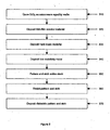
- FIG. 3 there is illustrated a method of fabricating, by simultaneous formation, a resistor and bottom electrode of a micro-electromechanical switch in accordance with the present invention.
- an anchor material such as SiO 2 is grown (or deposited) on a microwave quality wafer or substrate.
- Figure 4 illustrates a preferred embodiment of a growth deposit of SiO 2 on a silicon substrate, however, the substrate can be made of various materials, for example, silicon on sapphire, gallium arsenide, alumina, glass, silicon on insulator, etc.
- Formation of the switch on a thick oxide region on a silicon substrate permits control circuitry for control electrodes to be integrated on the same die as the switch. The oxide also helps reduce dielectric losses associate with the silicon substrate.
- a thin-film resistor material is deposited.
- the details for the fabrication of thin-film resistors using metals such as TaN, SiCr, or NiCr are set forth in U.S. Patent Application Serial No. 09/452,691 filed 12/02/1999, Baiely et al., the disclosure of which is incorporated herein by reference. Use of NiCr will be considered here, although any of the other above-mentioned materials can be used. NiCr is used as the thin-film resistor material in the preferred embodiment.
- a hard mask material adapted from generally known micro-fabrication techniques is deposited in a subsequent act 330 over the NiCr layer.
- a hard mask material adapted from generally known micro-fabrication techniques is deposited in a subsequent act 330 over the NiCr layer.
- approximately 1000 ⁇ of TiW is deposited in deposition act 330.
- a low resistivity metal is deposited.
- Al-Si is deposited to a thickness required for optimized RF operation of the switch. Generally, approximately 4000 ⁇ of Al-Si is sufficient.
- the entire stack of substrate, silicon dioxide, NiCr, TiW and Al-Si will serve as the switch bottom electrode and bias resistor.
- each layer is uniform.
- Figure 6A illustrates the bottom electrode 610, resistor 620, interconnect 630 and a bond pad 640 which have been patterned and etched, in accordance with the present invention, defining bottom electrode and resistor lengths
- Figure 6B illustrates a cross section view of Figure 6A through AA.
- the preferred stack of Al, TiW and NiCr, the Al can be either wet or dry etched while the TiW and NiCr are wet etched in a preferred embodiment.
- the next step 360 is a resist pattern which exposes the resistor to an etch which removes the hard mask materials (e.g. Al and TiW in this case).
- Figure 7A illustrates the bottom electrode 610 and resistor 620 after the Al and TiW have been removed and
- Figure 7B illustrates a cross section view of Figure 7A through AA. Note that the bottom electrode is not affected by this second etch step 360 (it is completely covered with resist).
- a primary capacitor dielectric is deposited on the bottom electrode and patterned and etched 370.
- the primary dielectric is SiO 2 , Si 3 N 4 or Ta 2 O 5 , for example, although the use of any suitable dielectric is foreseen.
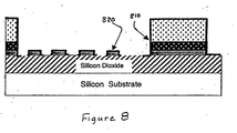
- Figure 8 illustrates the bottom electrode and resistor structure following the dielectric deposit, pattern and etch.
- Item 810 shows the dielectric covering the bottom electrode and item 820 shows the dielectric covering part of the resistor. It is recommended that the exposed resistor material be encapsulated as soon as possible following the removal of the hard mask material.
Landscapes
- Physics & Mathematics (AREA)
- Electromagnetism (AREA)
- Semiconductor Integrated Circuits (AREA)
- Non-Adjustable Resistors (AREA)
- Micromachines (AREA)
Applications Claiming Priority (2)
| Application Number | Priority Date | Filing Date | Title |
|---|---|---|---|
| US941031 | 2001-08-28 | ||
| US09/941,031 US6698082B2 (en) | 2001-08-28 | 2001-08-28 | Micro-electromechanical switch fabricated by simultaneous formation of a resistor and bottom electrode |
Publications (2)
| Publication Number | Publication Date |
|---|---|
| EP1288977A1 true EP1288977A1 (fr) | 2003-03-05 |
| EP1288977B1 EP1288977B1 (fr) | 2009-11-11 |
Family
ID=25475826
Family Applications (1)
| Application Number | Title | Priority Date | Filing Date |
|---|---|---|---|
| EP02102230A Expired - Lifetime EP1288977B1 (fr) | 2001-08-28 | 2002-08-28 | Elements de dispositifs de systèmes mécaniques microélectriques avec résistance à couches minces couplé à une électrode de contact |
Country Status (4)
| Country | Link |
|---|---|
| US (2) | US6698082B2 (fr) |
| EP (1) | EP1288977B1 (fr) |
| JP (1) | JP2003179401A (fr) |
| DE (1) | DE60234295D1 (fr) |
Cited By (1)
| Publication number | Priority date | Publication date | Assignee | Title |
|---|---|---|---|---|
| WO2006012253A1 (fr) * | 2004-06-29 | 2006-02-02 | Intel Corporation | Mecanisme pour empecher un auto-actionnement dans un commutateur microelectromecanique |
Families Citing this family (27)
| Publication number | Priority date | Publication date | Assignee | Title |
|---|---|---|---|---|
| US6698082B2 (en) * | 2001-08-28 | 2004-03-02 | Texas Instruments Incorporated | Micro-electromechanical switch fabricated by simultaneous formation of a resistor and bottom electrode |
| US6804502B2 (en) | 2001-10-10 | 2004-10-12 | Peregrine Semiconductor Corporation | Switch circuit and method of switching radio frequency signals |
| JP4659826B2 (ja) | 2004-06-23 | 2011-03-30 | ペレグリン セミコンダクター コーポレーション | Rfフロントエンド集積回路 |
| WO2006033271A1 (fr) * | 2004-09-22 | 2006-03-30 | Advantest Corporation | Dispositif de circuit haute frequence |
| US9653601B2 (en) | 2005-07-11 | 2017-05-16 | Peregrine Semiconductor Corporation | Method and apparatus for use in improving linearity of MOSFETs using an accumulated charge sink-harmonic wrinkle reduction |
| US8742502B2 (en) | 2005-07-11 | 2014-06-03 | Peregrine Semiconductor Corporation | Method and apparatus for use in improving linearity of MOSFETs using an accumulated charge sink-harmonic wrinkle reduction |
| USRE48965E1 (en) | 2005-07-11 | 2022-03-08 | Psemi Corporation | Method and apparatus improving gate oxide reliability by controlling accumulated charge |
| US7910993B2 (en) | 2005-07-11 | 2011-03-22 | Peregrine Semiconductor Corporation | Method and apparatus for use in improving linearity of MOSFET's using an accumulated charge sink |
| US7890891B2 (en) | 2005-07-11 | 2011-02-15 | Peregrine Semiconductor Corporation | Method and apparatus improving gate oxide reliability by controlling accumulated charge |
| US20080076371A1 (en) | 2005-07-11 | 2008-03-27 | Alexander Dribinsky | Circuit and method for controlling charge injection in radio frequency switches |
| US7602265B2 (en) * | 2005-10-20 | 2009-10-13 | International Business Machines Corporation | Apparatus for accurate and efficient quality and reliability evaluation of micro electromechanical systems |
| US7463123B2 (en) * | 2005-11-22 | 2008-12-09 | University Of South Florida | Nanometer electromechanical switch and fabrication process |
| US7960772B2 (en) * | 2007-04-26 | 2011-06-14 | Peregrine Semiconductor Corporation | Tuning capacitance to enhance FET stack voltage withstand |
| JP5417346B2 (ja) | 2008-02-28 | 2014-02-12 | ペレグリン セミコンダクター コーポレーション | 集積回路素子内でキャパシタをデジタル処理で同調するときに用いられる方法及び装置 |
| US8410658B2 (en) * | 2008-05-30 | 2013-04-02 | Gang Zhang | Multi-layer electrostatic energy harvester and method of making the same |
| JP5374077B2 (ja) * | 2008-06-16 | 2013-12-25 | ローム株式会社 | Memsセンサ |
| JP2010098518A (ja) * | 2008-10-16 | 2010-04-30 | Rohm Co Ltd | Memsセンサの製造方法およびmemsセンサ |
| US8723260B1 (en) | 2009-03-12 | 2014-05-13 | Rf Micro Devices, Inc. | Semiconductor radio frequency switch with body contact |
| US9590674B2 (en) | 2012-12-14 | 2017-03-07 | Peregrine Semiconductor Corporation | Semiconductor devices with switchable ground-body connection |
| US20150236748A1 (en) | 2013-03-14 | 2015-08-20 | Peregrine Semiconductor Corporation | Devices and Methods for Duplexer Loss Reduction |
| US9406695B2 (en) | 2013-11-20 | 2016-08-02 | Peregrine Semiconductor Corporation | Circuit and method for improving ESD tolerance and switching speed |
| US9831857B2 (en) | 2015-03-11 | 2017-11-28 | Peregrine Semiconductor Corporation | Power splitter with programmable output phase shift |
| US9948281B2 (en) | 2016-09-02 | 2018-04-17 | Peregrine Semiconductor Corporation | Positive logic digitally tunable capacitor |
| US10886911B2 (en) | 2018-03-28 | 2021-01-05 | Psemi Corporation | Stacked FET switch bias ladders |
| US10505530B2 (en) | 2018-03-28 | 2019-12-10 | Psemi Corporation | Positive logic switch with selectable DC blocking circuit |
| US10236872B1 (en) | 2018-03-28 | 2019-03-19 | Psemi Corporation | AC coupling modules for bias ladders |
| US11476849B2 (en) | 2020-01-06 | 2022-10-18 | Psemi Corporation | High power positive logic switch |
Citations (6)
| Publication number | Priority date | Publication date | Assignee | Title |
|---|---|---|---|---|
| US4959515A (en) * | 1984-05-01 | 1990-09-25 | The Foxboro Company | Micromechanical electric shunt and encoding devices made therefrom |
| DE4008832C1 (en) * | 1990-03-20 | 1991-07-18 | Rohde & Schwarz Gmbh & Co Kg, 8000 Muenchen, De | Microswitch operated by electrostatic force - has force electrode of resistance material between end contacts |
| US5356826A (en) * | 1992-08-07 | 1994-10-18 | Yamaha Corporation | Method of manufacturing semiconductor device provided with capacitor and resistor |
| EP0726597A2 (fr) * | 1995-02-13 | 1996-08-14 | Harris Corporation | Gravure directe pour résistance à couches minces utilisant un masque dur |
| DE19950373A1 (de) * | 1998-10-23 | 2000-04-27 | Rohde & Schwarz | Mikromechanisches Relais mit federndem Kontakt und Verfahren zum Herstellen desselben |
| US6376787B1 (en) * | 2000-08-24 | 2002-04-23 | Texas Instruments Incorporated | Microelectromechanical switch with fixed metal electrode/dielectric interface with a protective cap layer |
Family Cites Families (13)
| Publication number | Priority date | Publication date | Assignee | Title |
|---|---|---|---|---|
| USRE33651E (en) * | 1984-12-28 | 1991-07-30 | At&T Bell Laboratories | Variable gap device and method of manufacture |
| US5013396A (en) * | 1987-06-01 | 1991-05-07 | The Regents Of The University Of Michigan | Method of making an ultraminiature pressure sensor |
| US5207103A (en) * | 1987-06-01 | 1993-05-04 | Wise Kensall D | Ultraminiature single-crystal sensor with movable member |
| US5025346A (en) * | 1989-02-17 | 1991-06-18 | Regents Of The University Of California | Laterally driven resonant microstructures |
| US5407841A (en) * | 1992-10-30 | 1995-04-18 | Hughes Aircraft Company | CBiCMOS fabrication method using sacrificial gate poly |
| US5603847A (en) * | 1993-04-07 | 1997-02-18 | Zycon Corporation | Annular circuit components coupled with printed circuit board through-hole |
| US5619061A (en) * | 1993-07-27 | 1997-04-08 | Texas Instruments Incorporated | Micromechanical microwave switching |
| US5420063A (en) * | 1994-04-11 | 1995-05-30 | National Semiconductor Corporation | Method of producing a resistor in an integrated circuit |
| DE4414968A1 (de) * | 1994-04-28 | 1995-11-02 | Siemens Ag | Mikrosystem mit integrierter Schaltung und mikromechanischem Bauteil und Herstellverfahren |
| US5573679A (en) * | 1995-06-19 | 1996-11-12 | Alberta Microelectronic Centre | Fabrication of a surface micromachined capacitive microphone using a dry-etch process |
| US5778513A (en) * | 1996-02-09 | 1998-07-14 | Denny K. Miu | Bulk fabricated electromagnetic micro-relays/micro-switches and method of making same |
| US6326256B1 (en) * | 1998-12-18 | 2001-12-04 | Texas Instruments Incorporated | Method of producing a laser trimmable thin film resistor in an integrated circuit |
| US6698082B2 (en) * | 2001-08-28 | 2004-03-02 | Texas Instruments Incorporated | Micro-electromechanical switch fabricated by simultaneous formation of a resistor and bottom electrode |
-
2001
- 2001-08-28 US US09/941,031 patent/US6698082B2/en not_active Expired - Lifetime
-
2002
- 2002-08-27 JP JP2002247074A patent/JP2003179401A/ja active Pending
- 2002-08-28 EP EP02102230A patent/EP1288977B1/fr not_active Expired - Lifetime
- 2002-08-28 DE DE60234295T patent/DE60234295D1/de not_active Expired - Lifetime
-
2003
- 2003-08-18 US US10/642,969 patent/US6977196B1/en not_active Expired - Lifetime
Patent Citations (6)
| Publication number | Priority date | Publication date | Assignee | Title |
|---|---|---|---|---|
| US4959515A (en) * | 1984-05-01 | 1990-09-25 | The Foxboro Company | Micromechanical electric shunt and encoding devices made therefrom |
| DE4008832C1 (en) * | 1990-03-20 | 1991-07-18 | Rohde & Schwarz Gmbh & Co Kg, 8000 Muenchen, De | Microswitch operated by electrostatic force - has force electrode of resistance material between end contacts |
| US5356826A (en) * | 1992-08-07 | 1994-10-18 | Yamaha Corporation | Method of manufacturing semiconductor device provided with capacitor and resistor |
| EP0726597A2 (fr) * | 1995-02-13 | 1996-08-14 | Harris Corporation | Gravure directe pour résistance à couches minces utilisant un masque dur |
| DE19950373A1 (de) * | 1998-10-23 | 2000-04-27 | Rohde & Schwarz | Mikromechanisches Relais mit federndem Kontakt und Verfahren zum Herstellen desselben |
| US6376787B1 (en) * | 2000-08-24 | 2002-04-23 | Texas Instruments Incorporated | Microelectromechanical switch with fixed metal electrode/dielectric interface with a protective cap layer |
Cited By (3)
| Publication number | Priority date | Publication date | Assignee | Title |
|---|---|---|---|---|
| WO2006012253A1 (fr) * | 2004-06-29 | 2006-02-02 | Intel Corporation | Mecanisme pour empecher un auto-actionnement dans un commutateur microelectromecanique |
| US7042308B2 (en) | 2004-06-29 | 2006-05-09 | Intel Corporation | Mechanism to prevent self-actuation in a microelectromechanical switch |
| CN1961397B (zh) * | 2004-06-29 | 2011-03-02 | 英特尔公司 | 微机电开关和用于防止微机电开关中的自启动的方法 |
Also Published As
| Publication number | Publication date |
|---|---|
| US6977196B1 (en) | 2005-12-20 |
| US20030042560A1 (en) | 2003-03-06 |
| DE60234295D1 (de) | 2009-12-24 |
| JP2003179401A (ja) | 2003-06-27 |
| EP1288977B1 (fr) | 2009-11-11 |
| US6698082B2 (en) | 2004-03-02 |
Similar Documents
| Publication | Publication Date | Title |
|---|---|---|
| EP1288977B1 (fr) | Elements de dispositifs de systèmes mécaniques microélectriques avec résistance à couches minces couplé à une électrode de contact | |
| US6525396B2 (en) | Selection of materials and dimensions for a micro-electromechanical switch for use in the RF regime | |
| US6046659A (en) | Design and fabrication of broadband surface-micromachined micro-electro-mechanical switches for microwave and millimeter-wave applications | |
| US5872489A (en) | Integrated tunable inductance network and method | |
| US6373007B1 (en) | Series and shunt mems RF switch | |
| EP0751546B2 (fr) | Micro-interrupteur électromécanique, pour fréquences radio | |
| US6646525B2 (en) | Microelectro-mechanical system actuator device and reconfigurable circuits utilizing same | |
| US6621392B1 (en) | Micro electromechanical switch having self-aligned spacers | |
| US7894205B2 (en) | Variable device circuit and method for manufacturing the same | |
| US6472962B1 (en) | Inductor-capacitor resonant RF switch | |
| US20070278075A1 (en) | Capacitance Type Mems Device, Manufacturing Method Thereof, And High Frequency Device | |
| US6486511B1 (en) | Solid state RF switch with high cutoff frequency | |
| US20030048149A1 (en) | MEMS RF switch with low actuation voltage | |
| US7118935B2 (en) | Bump style MEMS switch | |
| US20080217149A1 (en) | Integrated arrangement and method for production | |
| US7477884B2 (en) | Tri-state RF switch | |
| US7960662B2 (en) | Radiofrequency or hyperfrequency micro-switch structure and method for producing one such structure | |
| US7439117B2 (en) | Method for designing a micro electromechanical device with reduced self-actuation | |
| WO2003015128A2 (fr) | Commutateur electromecanique et procede de fabrication correspondant | |
| US20070108540A1 (en) | Micro-electromechanical switch, method of manufacturing an integrated circuit including at least one such switch, and an integrated circuit | |
| KR100339394B1 (ko) | 정전기력을 이용한 마이크로 스위치 및 제조 방법 | |
| KR100308054B1 (ko) | 마이크로 스위치 및 제조 방법 | |
| Park et al. | A 3-voltage actuated micromachined RF switch for telecommunications applications | |
| EP1675148B1 (fr) | Procédé de conception d'un dispositif micro-électromécanique avec auto-déclenchement réduit | |
| Yao et al. | Micromachined RF signal switching devices on high resistivity silicon substrates |
Legal Events
| Date | Code | Title | Description |
|---|---|---|---|
| PUAI | Public reference made under article 153(3) epc to a published international application that has entered the european phase |
Free format text: ORIGINAL CODE: 0009012 |
|
| AK | Designated contracting states |
Designated state(s): AT BE BG CH CY CZ DE DK EE ES FI FR GB GR IE IT LI LU MC NL PT SE SK TR Kind code of ref document: A1 Designated state(s): AT BE BG CH CY CZ DE DK EE ES FI FR GB GR IE IT LI LU MC NL PT SE SK TR |
|
| AX | Request for extension of the european patent |
Extension state: AL LT LV MK RO SI |
|
| 17P | Request for examination filed |
Effective date: 20030905 |
|
| AKX | Designation fees paid |
Designated state(s): DE FR GB |
|
| 17Q | First examination report despatched |
Effective date: 20040211 |
|
| 17Q | First examination report despatched |
Effective date: 20040211 |
|
| GRAP | Despatch of communication of intention to grant a patent |
Free format text: ORIGINAL CODE: EPIDOSNIGR1 |
|
| GRAS | Grant fee paid |
Free format text: ORIGINAL CODE: EPIDOSNIGR3 |
|
| GRAA | (expected) grant |
Free format text: ORIGINAL CODE: 0009210 |
|
| AK | Designated contracting states |
Kind code of ref document: B1 Designated state(s): DE FR GB |
|
| REG | Reference to a national code |
Ref country code: GB Ref legal event code: FG4D |
|
| REF | Corresponds to: |
Ref document number: 60234295 Country of ref document: DE Date of ref document: 20091224 Kind code of ref document: P |
|
| PLBE | No opposition filed within time limit |
Free format text: ORIGINAL CODE: 0009261 |
|
| STAA | Information on the status of an ep patent application or granted ep patent |
Free format text: STATUS: NO OPPOSITION FILED WITHIN TIME LIMIT |
|
| 26N | No opposition filed |
Effective date: 20100812 |
|
| REG | Reference to a national code |
Ref country code: FR Ref legal event code: PLFP Year of fee payment: 15 |
|
| REG | Reference to a national code |
Ref country code: FR Ref legal event code: PLFP Year of fee payment: 16 |
|
| PGFP | Annual fee paid to national office [announced via postgrant information from national office to epo] |
Ref country code: GB Payment date: 20170725 Year of fee payment: 16 Ref country code: DE Payment date: 20170825 Year of fee payment: 16 Ref country code: FR Payment date: 20170720 Year of fee payment: 16 |
|
| REG | Reference to a national code |
Ref country code: DE Ref legal event code: R119 Ref document number: 60234295 Country of ref document: DE |
|
| GBPC | Gb: european patent ceased through non-payment of renewal fee |
Effective date: 20180828 |
|
| PG25 | Lapsed in a contracting state [announced via postgrant information from national office to epo] |
Ref country code: DE Free format text: LAPSE BECAUSE OF NON-PAYMENT OF DUE FEES Effective date: 20190301 |
|
| PG25 | Lapsed in a contracting state [announced via postgrant information from national office to epo] |
Ref country code: FR Free format text: LAPSE BECAUSE OF NON-PAYMENT OF DUE FEES Effective date: 20180831 |
|
| PG25 | Lapsed in a contracting state [announced via postgrant information from national office to epo] |
Ref country code: GB Free format text: LAPSE BECAUSE OF NON-PAYMENT OF DUE FEES Effective date: 20180828 |