EP1289005A2 - Verfahren zur Herstellung eines Bipolartransistors mit selbstjustierten Emitter und Basis - Google Patents
Verfahren zur Herstellung eines Bipolartransistors mit selbstjustierten Emitter und Basis Download PDFInfo
- Publication number
- EP1289005A2 EP1289005A2 EP02018974A EP02018974A EP1289005A2 EP 1289005 A2 EP1289005 A2 EP 1289005A2 EP 02018974 A EP02018974 A EP 02018974A EP 02018974 A EP02018974 A EP 02018974A EP 1289005 A2 EP1289005 A2 EP 1289005A2
- Authority
- EP
- European Patent Office
- Prior art keywords
- oxide film
- etching
- opening
- emitter
- base
- Prior art date
- Legal status (The legal status is an assumption and is not a legal conclusion. Google has not performed a legal analysis and makes no representation as to the accuracy of the status listed.)
- Withdrawn
Links
Images


Classifications
-
- H—ELECTRICITY
- H10—SEMICONDUCTOR DEVICES; ELECTRIC SOLID-STATE DEVICES NOT OTHERWISE PROVIDED FOR
- H10D—INORGANIC ELECTRIC SEMICONDUCTOR DEVICES
- H10D10/00—Bipolar junction transistors [BJT]
- H10D10/01—Manufacture or treatment
- H10D10/051—Manufacture or treatment of vertical BJTs
-
- H—ELECTRICITY
- H10—SEMICONDUCTOR DEVICES; ELECTRIC SOLID-STATE DEVICES NOT OTHERWISE PROVIDED FOR
- H10D—INORGANIC ELECTRIC SEMICONDUCTOR DEVICES
- H10D10/00—Bipolar junction transistors [BJT]
- H10D10/40—Vertical BJTs
- H10D10/421—Vertical BJTs having both emitter-base and base-collector junctions ending at the same surface of the body
-
- H—ELECTRICITY
- H10—SEMICONDUCTOR DEVICES; ELECTRIC SOLID-STATE DEVICES NOT OTHERWISE PROVIDED FOR
- H10D—INORGANIC ELECTRIC SEMICONDUCTOR DEVICES
- H10D62/00—Semiconductor bodies, or regions thereof, of devices having potential barriers
- H10D62/10—Shapes, relative sizes or dispositions of the regions of the semiconductor bodies; Shapes of the semiconductor bodies
- H10D62/13—Semiconductor regions connected to electrodes carrying current to be rectified, amplified or switched, e.g. source or drain regions
- H10D62/133—Emitter regions of BJTs
-
- H—ELECTRICITY
- H10—SEMICONDUCTOR DEVICES; ELECTRIC SOLID-STATE DEVICES NOT OTHERWISE PROVIDED FOR
- H10D—INORGANIC ELECTRIC SEMICONDUCTOR DEVICES
- H10D62/00—Semiconductor bodies, or regions thereof, of devices having potential barriers
- H10D62/10—Shapes, relative sizes or dispositions of the regions of the semiconductor bodies; Shapes of the semiconductor bodies
- H10D62/17—Semiconductor regions connected to electrodes not carrying current to be rectified, amplified or switched, e.g. channel regions
- H10D62/177—Base regions of bipolar transistors, e.g. BJTs or IGBTs
-
- H—ELECTRICITY
- H10—SEMICONDUCTOR DEVICES; ELECTRIC SOLID-STATE DEVICES NOT OTHERWISE PROVIDED FOR
- H10D—INORGANIC ELECTRIC SEMICONDUCTOR DEVICES
- H10D64/00—Electrodes of devices having potential barriers
- H10D64/20—Electrodes characterised by their shapes, relative sizes or dispositions
- H10D64/23—Electrodes carrying the current to be rectified, amplified, oscillated or switched, e.g. sources, drains, anodes or cathodes
- H10D64/231—Emitter or collector electrodes for bipolar transistors
Definitions
- the present invention relates to a method for fabricating a bipolar transistor having self-aligned base and emitter.
- the present invention also relates to such a semiconductor device.
- bipolar transistors Semiconductor deices including therein bipolar transistors have been developed to achieve higher-speed and higher-performance operation. This development is attempted by using finer patterning techniques, wherein the parasitic capacitance and the base resistance of the bipolar transistor are reduced while reducing the junction depth thereof to thereby reduce the transit time of the carriers.
- One of such patterning techniques is a self-alignment fabrication technique for a bipolar transistor, wherein the emitter region and the base region are separated in a self-alignment scheme, and impurities are introduced from the base lead electrode formed in the periphery of the bipolar transistor to form an external base (or graft base) on the outer periphery of the base region.
- a bipolar transistor having such a self-alignment structure it is important to reduce the effective emitter width for obtaining excellent high-frequency characteristics such as a steep cut-off frequency (fT) and a high oscillation frequency (fmax).
- fT steep cut-off frequency
- fmax high oscillation frequency
- BVebo breakdown voltage
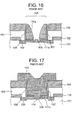
- Figs. 14 to 18 consecutively show steps of a conventional fabrication process for a semiconductor device having a self-aligned bipolar transistor.
- the process begins with a silicon substrate 101 on which a first silicon oxide film 102 is formed by a thermal oxidation technique, followed by selectively etching a portion of the first silicon oxide film 102 on the emitter region (region for forming the emitter) and the intrinsic base region (region for forming the intrinsic base 108) by using a photolithographic technique.
- a first polysilicon layer 103 is deposited on the first silicon oxide film 102 by using a CVD technique, followed by implanting boron ions into the first polysilicon layer 103 by using an ion-implantation technique.
- the first polysilicon layer 103 is selectively etched using a photolithographic technique, followed by deposition of a first silicon nitride film 104 by using a CVD technique on both the first polysilicon layer 103 and the first silicon oxide film 102 exposed from the etched first polysilicon layer 103. Subsequently, the first polysilicon layer 103 and the first silicon nitride film 104 are selectively etched to form an opening 105 which exposes the base region other than a graft base region.
- a second silicon oxide film 106 is formed using a thermal oxidation technique on the wall and the bottom of the opening 105, the second silicon oxide film 106 serving as a diffusion assist layer.
- boron ions are implanted through the bottom of the second silicon oxide film 106 into the silicon substrate 101 by using an ion-implantation technique, thereby forming an intrinsic base 108.
- a second silicon nitride film 107 is then deposited in the opening 105 by using a CVD technique, followed by depositing a second polysilicon layer 110 on the first silicon nitride film 104 in the opening 105, as shown in Fig. 14.
- the second polysilicon layer 110 is selectively removed by an anisotropic dry etching technique, to leave a first side-wall polysilicon layer 110a on the second silicon nitride film 107 in the opening 105.
- the anisotropic dry etching is conducted using reactive ions under the gas ambient wherein the etch rate for the polysilicon layer is larger compared to the etch rate for the silicon nitride film.
- the gas ambient is such that Cl 2 , HBr and He are introduced at flow rates of 5 to 50sccm (standard cubic centimeters), 10 to 100sccm and 1 to 10sccm, respectively, for example.
- the ions reflected by the first side-wall polysilicon layer 110a in the opening 105 are concentrated on the bottom of the inner side of the polysilicon layer 110a, thereby increasing the etched amount of the bottom of the opening 105 to form a trench 111 on the bottom.
- the trench 111 may penetrate the second silicon nitride film 107 to reach the second silicon oxide film 106, as shown in Fig. 15.
- the thick second silicon nitride film 107 reduces the aspect ratio of the opening 105 for preventing occurrence of voids in the polysilicon layer etc. in the opening 105, sufficient over-etching is not conducted for the thick second silicon nitride film 107 for avoiding a larger depth for the trench 111.
- another anisotropic dry etching process is conducted using the first side-wall polysilicon layer 110a as a mask to remove a portion of the second silicon nitride film 107 on the emitter region.
- the gas ambient in the another anisotropic dry etching is such that the etch rate for the silicon nitride film is larger than the etch rate for the silicon oxide film.
- SF 6 and He are introduced during the another anisotropic dry etching at flow rates of 40 to 200sccm and 50 to 250sccm, respectively, while using reactive ions.
- the another dry etching increases the depth of the trench 111 to form a deep trench 111a, which penetrates the second silicon oxide film 106 to reach the intrinsic base 108.
- wet etching is conducted using a mixture of HF, HNO 3 and CH 3 COOH to remove the first side-wall polysilicon layer 110a within the opening 105, further increasing the depth of the trench 111a which has already reached the intrinsic base 108.
- a portion of the second silicon oxide film 106 on the emitter region is removed by wet etching using a hydrofluoric acid based liquid.
- the native oxide film on the intrinsic base region is removed by using a hydrofluoric acid based liquid, followed by depositing a second polysilicon layer 113 while introducing SiH4 gas into the deposition chamber.
- Arsenic ions are then introduced into the second polysilicon layer 113 by using an ion-implantation technique.
- an emitter injection treatment is conducted wherein an emitter 114 is formed by diffusing the arsenic ions in the third polysilicon layer 113 toward the intrinsic base 108 by solid phase diffusion.
- an emitter injection treatment although the trench 111a filled with the third polysilicon layer 113 does not penetrate the intrinsic base 108, there is some possibility depending on the process conditions that the diffused ions allow the trench 111a to electrically penetrate the intrinsic base 108 while diffusing toward the silicon substrate 101 which constitutes the collector. Thereafter, a portion of the second polysilicon layer 113 is selectively removed.
- a first interlayer dielectric film 115 is formed on the first silicon nitride film 104 and the second polysilicon layer 113, followed by selectively etching thereof on the second polysilicon layer 113 and forming consecutively an emitter barrier metal layer 119 having a hollow cylindrical shape and an emitter lead electrode 120 having a solid cylindrical shape.
- an emitter electrode 121 having a planar size larger than the planar size of the emitter barrier metal layer 119 is formed on top of the emitter lead electrode 120.
- a base barrier metal layer 116, a base lead electrode 117 and a base electrode 118 as well as a collector barrier metal layer 122, a collector lead electrode 123 and a collector electrode 124 are formed to obtain the structure of the bipolar transistor shown in Fig. 18.
- the trench 111a electrically penetrates the intrinsic base 108, a short circuit failure occurs between the collector and the emitter to prevent a normal device operation of the bipolar transistor. Even if the trench 111a does not electrically penetrate the intrinsic base 108, the emitter 114 formed on the planar surface of the intrinsic base 108 does not allow a sufficient large distance between the emitter 114 and the graft base 109. This reduces the breakdown voltage of the emitter-base junction (BVebo) down to as low as 1.8 volts, for example.
- BVebo breakdown voltage of the emitter-base junction
- Patent Publication JP-A-7-307347 Another conventional technique is also described in Patent Publication JP-A-7-307347.
- the self-aligned bipolar transistor is fabricated by using an isotropic dry etching technique wherein an epitaxial base layer having an opening is etched by a 3 to 9nm depth.
- the isotropic dry etching used in this technique reduces the damage on the base layer compared to the case of using the anisotropic dry etching, there arises another problem in that the plasma or electrons generated during the isotropic dry etching step generates crystal defects which cause generation and recombination of carriers to thereby increase the low-frequency noise in the resultant bipolar transistor.
- Earlier JP Patent Application 2000-071181 also proposes a technique using an isotropic dry etching step in fabrication of the self-aligned bipolar transistor, wherein an epitaxial base layer in an opening is etched.
- the proposed technique does not remove the damage caused by the isotropic dry etching on the base, although this technique has an advantage in that the electrostatic breakdown voltage can be improved without increasing the base-collector capacitance.
- JP-A-9-172064 Another conventional technique is described in JP-A-9-172064, wherein the fabrication step for forming the side-wall is conducted twice separately to obtain a two-layer structure for the side-wall in an insulated-gate transistor, such as a longitudinal MOSFET, having a trench.
- an anisotropic dry etching using the side-wall having the two-layer structure as a mask, a trench is formed in the silicon substrate by reactive ions.
- JP-A-9-172064 is applied to forming a semiconductor device having the self-aligned bipolar transistor, an advantage of smaller effective emitter size may be obtained.
- the ions reflected by the wall of the opening in the anisotropic dry etching are concentrated on the bottom edge of the opening to form a trench, similarly to the conventional technique described with reference to Figs. 14 to 18.
- the trench may allow the arsenic ions to diffuse and reach the silicon substrate constituting the collector during the emitter injection treatment for forming the emitter, whereby a short-circuit failure occurs between the emitter and the collector and thus a normal device operation cannot be obtained.
- the present invention provides a method for fabricating a bipolar transistor in a semiconductor device, the method including the steps of: forming a silicon layer on a semiconductor substrate; selectively etching the silicon layer to form an opening for exposing a first portion of the semiconductor substrate; conducting a combination etching to the first portion to form a concave surface thereon, the combination etching including consecutive isotropic dry etching and wet etching; implanting first-conductivity type impurities through the concave surface to the first portion to form an intrinsic base; and implanting second-conductivity type impurities into a surface portion of the intrinsic base to form an emitter on the intrinsic base.
- the crystal defects associated with the generation and recombination of carriers can be reduced to thereby suppress the low-frequency noise.
- the consecutive isotropic dry etching and wet etching allows the bottom surface of the opening having a trench to assume a smooth concave surface.
- the emitter formed on the concave surface which constitutes the intrinsic base allows a larger distance to be obtained between the central intrinsic base and the peripheral emitter due to the concave surface compared to the distance obtained in the case of the planar surface of the intrinsic base such as in the conventional technique.
- the larger distance raises the emitter-base breakdown voltage, whereas the concave surface of the intrinsic base alleviates the concentration of the current which has otherwise a tendency to flow the corner of the intrinsic base in the vicinity of the graft base region.
- the first and second conductivity types may be p-type and n-type, respectively, or vice versa.
- the present invention also provides a semiconductor device including a bipolar transistor having self-aligned emitter and base, the semiconductor device including: a semiconductor substrate; a silicon layer formed on the semiconductor substrate; an opening formed in the silicon layer for exposing an area in which the self-aligned emitter and base are formed; and a side-wall oxide film formed on bottom and wall of the opening.
- the semiconductor device of the present invention can be manufactured by the method of the present invention, and achieve the advantages of suppression of occurrence of voids in the silicon layer.
- the silicon layer may be preferably a polysilicon layer.
- self-aligned bipolar transistor means the structure wherein the opening formed for forming the base of the bipolar transistor is used to define the location of the emitter with respect to the base.
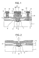
- a bipolar transistor is formed in a semiconductor device, which includes a silicon substrate 1, on which a first silicon oxide film 2, a first polysilicon layer 3, a first silicon nitride film 4 and a first interlayer dielectric film 15 are consecutively formed.
- An intrinsic base 8 and an emitter 14 are consecutively formed in the central area or the bipolar transistor, and a second silicon oxide film 6 and a second silicon nitride film 7 are consecutively formed on the emitter 14.
- a graft base or external base 9 is formed on the outer periphery of the intrinsic base 8.
- a second polysilicon layer 13 is formed within and above an opening 5 formed in the first polysilicon layer 3, which has an inner wall covered by the second silicon nitride film 7.
- An emitter lead electrode 20 is formed on the second polysilicon layer 13 with an intervention of an emitter barrier metal layer 19, and an emitter electrode 21 is formed on the emitter lead electrode 20.
- a base barrier metal layer 16 with a hollow cylindrical shape having a bottom in contact with the first polysilicon layer 3 is formed on one of the edges of the bipolar transistor as a contact plug, penetrating the first interlayer dielectric film 15 and the first silicon nitride film 4.
- a cylindrical base lead electrode 17 is formed within the base barrier metal layer 16, and has a top on which a base electrode 18 is formed.
- a collector barrier metal layer 22 with a hollow cylindrical shape having a bottom in contact with the silicon substrate 1 is formed on the opposing edge of the bipolar transistor as a contact plug, penetrating the first silicon nitride film 4 and the silicon oxide film 2.
- a cylindrical collector lead electrode 23 is formed within the collector barrier metal layer 22, having a top on which a collector electrode 24 is formed.
- the process begins with a silicon substrate 1 doped with phosphorous at an impurity concentration of 2.0 ⁇ 10 17 cm -3 , on which a first silicon oxide film 2 is formed by a thermal oxidation technique. A portion of the first silicon oxide film 2 is selectively etched by an ordinary photolithographic etching technique to have an opening exposing a region for the base and emitter.
- a first polysilicon layer 3 is formed on the first silicon oxide film 2 by a CVD technique, followed by implanting boron into the first silicon polysilicon layer 3 by ion-implantation, for example, at an acceleration energy of 10 to 20 keV with a dosage of 1 ⁇ 10 15 to 8 ⁇ 10 15 cm -2 .
- first polysilicon layer 3 on the region for the collector lead electrode 23 is selectively etched by an ordinary photolithographic etching technique.
- a first silicon nitride film 4 is then formed by a CVD technique on the first polysilicon layer 3 and the first silicon oxide film 2 exposed from the first polysilicon layer 3.
- the first polysilicon layer 3 and the silicon nitride film 4 are selectively etched to form an opening 5 exposing the base region except for the graft base 9 by using an ordinary photolithographic etching technique.
- an isotropic dry etching process is conducted for the silicon substrate 1 exposed from the opening 5, wherein the etch rate is higher for silicon and lower for silicon nitride.
- This etch rate is obtained mainly by radicals in plasma wherein CF 4 and O 2 are introduced at flow rates of 30 to 150sccm and 80 to 300sccm, respectively, at a chamber pressure of 10 to 200Pa. The etch rate alleviates the damage of the silicon substrate 1.
- a wet etching process is conducted to further etch the silicon substrate 1, thereby removing the damage of the silicon substrate 1 caused by the isotropic dry etching for the intrinsic base in the opening 5.
- the wet etching uses, for example, a mixture of HF, HNO 3 and CH 3 COOH as an etchant.
- the combination etching including consecutive isotropic dry etching and wet etching allows the surface of the silicon substrate 1 to form a smooth concave depression having a depth of 20 to 100mm at a maximum.
- the presence of the smooth concave depression on the region for forming the base layer prevents the base-to-collector current from being concentrated in the vicinity of the graft base 9 in the resultant bipolar transistor.
- a thermal oxidation process is then conducted to form a second silicon oxide film 6 on the wall and bottom of the opening 5.
- the impurity (phosphorous) concentration of the silicon substrate 1 is lower than 2.0 ⁇ 10 17 cm -3
- a collector layer having an impurity concentration of about 2.0 X 10 17 cm -3 should be formed in the silicon substrate 1.
- phosphorous ions may be implanted through the second silicon oxide film 6 into the silicon substrate 1. This ion-implantation my be such that phosphorous ions, for example, are accelerated at an acceleration energy of 250 to 350 keV and implanted at a dosage of 4 ⁇ 10 12 cm -2 to 6 ⁇ 10 12 cm -2 .
- an ion-implantation process is conducted wherein boron ions are implanted through the second silicon oxide film 6 into the silicon substrate 1 to form the intrinsic base 8. Further, an annealing process is conducted to remedy the crystal defects caused by this ion-implantation, thereby diffusing the boron ions in the first polysilicon layer 3 toward the silicon substrate 1 to form the graft base 9. Thereafter, a second silicon nitride film 7 is formed by a CVD technique on the second silicon oxide film 6 in the opening 5.
- the process for forming the intrinsic base 8 may use the conditions proposed in JP Patent Application 2000-350796, and the boron concentration of the graft base 9 may be 1 ⁇ 10 21 to 2 ⁇ 10 21 cm -3 .
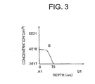
- a boron concentration profile of the intrinsic base 8 as viewed along the line A1-B1 in Fig. 2 after the annealing process.
- the boron concentration profile is obtained by secondary ion mass spectroscopy (SIMS).
- SIMS secondary ion mass spectroscopy
- the boron concentration resides at 4 ⁇ 10 18 cm -3 at the top, and reduces down to 2 ⁇ 10 17 cm -3 at the depth somewhat below 70nm from the top.
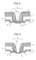
- a third silicon oxide film 10 is formed on the first silicon nitride film 4 and in the opening 5 by a CVD process, wherein TEOS, O 2 , He and Ar are introduced at flow rates of 80 to 200sccm, 1 to 10sccm, 150 to 300sccm, and 40 to 200sccm, respectively, at a chamber pressure of 200 to 800Pa. These process conditions achieve excellent coverage for the third silicon nitride film 10.
- a first anisotropic dry etching process is conducted to etch a portion of the third silicon oxide 10 constituting the wall of the opening 5 to leave a first side-wall oxide film 10a.
- the first anisotropic dry etching is such that the etch rate for silicon oxide is higher than the etch rate for silicon nitride.
- CF 4 , CHF 3 and He are introduced into the chamber at flow rates of 10 to 200sccm, 10 to 200sccm and 20 to 300sccm, respectively, while using reactive ions.
- the ions reflected by the wall of the opening 5 are concentrated onto the bottom edge of the opening 5, thereby forming a trench 11 at the bottom edge due to a large amount of etching.
- the etching for the side-wall oxide film 10a is stopped and a silica film is formed by coating in the trench, followed by baking thereof to form a step-alleviation film 12 which alleviates the step formed by the trench 11.
- a second anisotropic dry etching process similar to the first anisotropic dry etching process is conducted to the first side-wall oxide film 10a, whereby the step-alleviation film 12 on the emitter region and the third silicon oxide film 10 on the first silicon nitride film 4 are removed.
- the presence of the step-alleviation film 12 allows the second silicon nitride film 7 at the bottom of the cylinder to be removed, whereby the surface of the second silicon oxide film 6 is subjected to uniform over-etching, the cylinder being defined by the first side-wall oxide film. 10a at this stage.
- a third anisotropic dry etching process is conducted using the first side-wall oxide film 10a as a mask, thereby removing the second silicon oxide film 6 on the emitter region.
- the process conditions for the third anisotropic dry etching are such that the etch rate for silicon nitride is higher than the etch rate for silicon oxide.
- SF 6 and He are introduced at flow rates of 40 to 200sccm and 50 to 250sccm, respectively, while using reactive ions for etching.
- a portion of the second silicon oxide film 6 on the emitter region is removed by wet etching under the etching conditions that render the effective emitter width X to be minimum.
- This wet etching uses a hydrofluoric acid based liquid, for example.
- a portion of the first side-wall oxide film 10a is left as a second side-wall oxide film 10b on the wall of the opening 5.
- a native oxide film formed on the surface of the intrinsic base 8 is removed by wet etching using a hydrofluoric acid based liquid, followed by depositing a second polysilicon layer 13 to fill the opening 5 while introducing SiH 4 gas etc. into the chamber.
- the second polysilicon layer 13 is then doped with arsenic ions by using an ion-implantation technique.
- an emitter injection treatment is conducted using a lamp anneal technique, wherein arsenic ions in the second polysilicon layer 13 are thermally diffused through the opening of the second silicon oxide film 6 toward the surface of the intrinsic base 8 exposed from the opening 5, thereby forming the emitter 14.
- the lamp anneal process may use the conditions described in JP Patent Application 2000-350796.
- Fig. 7 shows the results of SIMS for detecting the boron and arsenic profiles of the second polysilicon layer 13 and the intrinsic base 8 after the emitter injection treatment, as viewed along line A2-B2 of Fig. 6.
- the arsenic concentration of the second polysilicon layer 13 resides at 1 ⁇ 10 21 cm -3 at a depth of 0nm and reduces down to 2 ⁇ 10 17 cm -3 at the depth somewhat below 0nm, whereas the boron concentration of the silicon substrate 1 resides at 4 ⁇ 10 18 cm -3 at a depth of 0nm and reduces down to 2 ⁇ 10 17 cm -3 at a depth of 70nm.
- a first interlayer dielectric film 15 is formed on the first silicon nitride film 4 and the second polysilicon layer 13.
- the first interlayer dielectric film 15 may be any insulator film and is a BPSG (boron-phosphor-silicate glass) film, for example, in this embodiment.
- the BPSG film is formed conveniently under a low temperature range, and has a higher capability for alleviating a step difference of the underlying film.
- a through-hole having a diameter smaller than the outer diameter of the second polysilicon layer 13 is formed in the first interlayer dielectric film 15 for later receiving therein an emitter electrode.
- An emitter barrier metal layer 19 is deposited on the bottom and the inner wall of the through-hole, followed by forming an emitter lead electrode 20 filling the through-hole on the emitter barrier metal layer 19.
- the emitter lead electrode 20 has a top surface flush with the top of the first interlayer dielectric film 15.
- an emitter electrode 21 having a planar size larger than the outer size of the emitter barrier metal layer 19 is formed on top of the emitter lead electrode 20.
- a base barrier metal layer 16, a base lead electrode 17 and a base electrode 18 as well as a collector barrier metal layer 22, a collector lead electrode 23 and a collector electrode 24 are formed as the electrode structures of the base and collector, to obtain a bipolar transistor in the semiconductor device.
- the barrier metal layers 16, 19 and 22 may be made of titanium, tungsten, a nitride of one of transition metals, and a silicide of boron, carbide etc.
- each of the barrier metal layers 16, 19 and 22 is made of titanium/titanium nitride films.
- Each of the base lead electrode 17, emitter lead electrode 20 and collector lead electrode 23 may be made of titanium or tungsten, and is made of tungsten in this example.
- Each of the base electrode 18, emitter electrode 21 and collector electrode 24 may be made of gold, silver, aluminum, an alloy of aluminum and barrier metal, an alloy of aluminum, copper and silicon, an alloy of copper, gold and barrier metal, an alloy of gold and barrier metal etc., and is made of an alloy of aluminum, copper and silicon in this example.
- a collector lead wire may be bonded directly onto the bottom surface of the silicon substrate 1. This renders the collector barrier metal layer 22, collector lead electrode 23 and collector electrode 24 unnecessary.
- the crystal defects causing generation and recombination of the carriers can be reduced to thereby suppress the low-frequency noise.
- the combination etching including the isotropic dry etching and wet etching forms a concave surface on the silicon substrate 1, the effective distance between the graft base 9 and the emitter 14 is increased without increasing the occupied area of the bipolar transistor, whereby the breakdown voltage of the emitter-base junction can be increased.
- the etched amount in the silicon substrate is smaller than the optimum amount, a sufficient breakdown voltage cannot be obtained for the emitter-base junction because the insufficient depth of the concave surface on the silicon substrate 1 reduces the distance between the graft base and the emitter.
- the operational frequency of the bipolar transistor is reduced because the excessive depth of the concave surface on the silicon substrate 1 increases the distance between the graft base 9 and the emitter 14 to raise the base resistance of the bipolar transistor.
- the second side-wall oxide film 10b left on the wall of the opening 5 in Fig. 6 has a function for improving the coverage in depositing the second polysilicon layer 13, emitter barrier metal layer 19 and emitter lead electrode 20. More specifically, the presence of the second side-wall oxide film 10b renders smooth the bridging portion between the bottom and the wall of the opening 5, thereby suppressing occurrence of voids, otherwise caused by the corner portion, during deposition of the second polysilicon layer 13, emitter barrier metal layer 19 and emitter lead electrode 20.
- the present embodiment provides an excellent structure wherein the emitter polysilicon layer 13 and emitter lead electrode 20 scarcely suffer from voids, even with an effective emitter width as small as 0.2 ⁇ m or smaller, thereby reducing the emitter resistance.
- the emitter arsenic profile having a depth of 20nm or less for an arsenic concentration of 2 ⁇ 10 17 cm -3 is formed in the case of the base profile having a depth of 70nm or less for a boron concentration of 2 ⁇ 10 17 cm -3 , then the base width is 50nm or less.
- the emitter has an effective emitter width of 0.2 ⁇ m or less, an emitter-base breakdown voltage of 2.7 volts can be obtained.
- the oscillator having a cut-off frequency (fT) of 43.2 GHz and a maximum oscillation frequency (fmax) of 42.4 GHz in the high-frequency characteristics thereof can be achieved for a collector-to-emitter voltage (Vce) of 1 volt.
- the concave surface of the silicon substrate 1 may be achieved by wet etching alone without using the isotropic dry etching after forming the opening.
- the etchant having a higher etch rate for silicon compared to the etch rate for silicon nitride may be a mixture of HF, HNO 3 and CH 3 COOH, which provides an etch depth of 20 to 100nm at a maximum for the concave surface.
- the wet etching alone may achieve further reduction of low-frequency noise compared to the combination etching.
- the fabrication steps of the present embodiment are similar to those of the first embodiment until the concave surface of the silicon substrate is obtained by using the combination etching.
- the intrinsic base is made of a compound semiconductor including Si, such as SiGe, instead of using ion-implantation.
- the present embodiment uses a lamp anneal process after the concave surface is formed, whereby boron ions in the first polysilicon layer 3 are diffused to the depression of the silicon substrate 1 by a solid phase diffusion to thereby form the graft base 9.
- the native oxide film on the silicon substrate 1 is removed using a hydrofluoric acid based liquid, followed by depositing a silicon-based compound semiconductor layer 25, such as including SiGe, in the opening 5 while adding boron.
- a fourth silicon oxide film 26 is deposited on the silicon-based compound semiconductor layer 25.
- the silicon-based compound semiconductor layer 25 such as including SiGe generally suffers from a problem in that the crystal strain is alleviated at a temperature of 1000 degrees C or above to thereby generate crystal misalignment and degrade in the crystallinity.
- the fourth silicon oxide film 26 should be deposited using a CVD technique wherein a lower temperature such as around 400 degrees C is appropriate for deposition.
- an ordinary etching process is conducted, wherein a portion of the fourth silicon oxide film 26 on the first silicon nitride film 4 is removed, to leave the fourth silicon oxide film 26 only in the opening 5, followed by depositing a second silicon nitride film 7 on the remaining fourth silicon nitride film 26.
- the subsequent steps are similar to those in the first embodiment.
- a method for fabricating a semiconductor device according to a third embodiment of the present invention will be described.
- the process for forming the oxide film on the wall of the opening 5 is conducted twice, thereby further reducing the effective emitter width and improving the emitter-base breakdown voltage.
- the processes are similar to those in the first embodiment until the step-alleviation film 12 is formed.
- Figs. 9 and 10 are enlarged sectional views of the opening 5 in the semiconductor device, consecutively showing the steps of fabrication process thereof.
- a fifth silicon oxide film 27 is deposited using a CVD technique on the third silicon oxide film 10 and the step-alleviation film 12.
- the conditions in this CVD process are similar to those used for forming the third silicon oxide film 10 in the first embodiment.
- a second anisotropic dry etching is conducted with the conditions similar to those in the first embodiment, to remove the fifth silicon oxide film 27, step-alleviation film 12 and the third silicon oxide film 10 on the emitter region.
- a third anisotropic dry etching is conducted with the conditions similar to those in the first embodiment, to remove the second silicon nitride film 7 on the emitter region while using the third side-wall oxide film 27a and the first side-wall oxide film 10a as a mask.
- the subsequent processes are similar to those in the first embodiment.
- a method according to a fourth embodiment of the present invention will be described.
- This embodiment achieves both reduction of the low-frequency noise and increase of the emitter-base breakdown voltage.
- the processes are similar to those in the first embodiment until the second silicon oxide film 6 is formed.
- ion-implantation is conducted to implant boron ions through the second silicon oxide film 6 to the silicon substrate 1, thereby forming an intrinsic base 8.
- an anneal treatment is conducted to remove the crystal defects caused by the ion-implantation, wherein boron ions in the first polysilicon layer 3 are diffused into the silicon substrate 1 to form a graft base 9.
- Another anneal treatment is then conducted to increase the depths of the intrinsic base 8 and the graft base 9 by diffusing the ions therein.
- the steps from the deposition of the second silicon nitride film 7 to the ion-implantation using arsenic ions are similar to those in the first embodiment.
- the arsenic ions in the second polysilicon layer 13 are diffused by a solid phase diffusion into the silicon substrate 1 to form the emitter 14, wherein the process conditions are such that the emitter having an arsenic concentration of 2 ⁇ 10 17 cm -3 has a thickness of 100nm or more.
- the subsequent steps are similar to those in the first embodiment.
- the low-frequency noise For reducing the low-frequency noise, it is important to suppress the generation and recombination of carriers. For this purpose, it is important to reduce the crystal defects causing the generation and recombination of carriers.
- the present inventors experimentally confirmed that the low-frequency noise could be reduced by forming the emitter at a depth of 100nm or more at which the crystal defects were significantly reduced compared to the location of a smaller depth.
- the deep emitter expands by diffusion also in the lateral direction, the concave surface of the silicon surface obtained by the isotropic dry etching increases the distance between the graft base 9 and the emitter 14, thereby increasing the emitter-base breakdown voltage in the bipolar transistor.
- the semiconductor device includes a silicon substrate 1, on which an n - -type epitaxial layer 29 is formed.
- the concave surface, on which the intrinsic base 8 and the emitter 14 is formed, is formed on the n - -type epitaxial layer 29.
- an n + -type buried layer 28 is provided between the silicon substrate 1 and the n - -type epitaxial layer 29, an n + -type buried layer 28 is provided.
- An n + -type collector lead layer 30 is formed between the n - -type epitaxial layer 29 and the bottom of the collector barrier metal layer 22.
- n + -type buried layer 28, n - -type epitaxial layer 29 and n + -type collector lead layer 30 reduces the collector resistance of the bipolar transistor.
- the constituent elements in the present embodiment other than the n + -type buried layer 28, n - -type epitaxial layer 29 and n+-type collector lead layer 30 are similar to those in the first embodiment.
Landscapes
- Bipolar Transistors (AREA)
Applications Claiming Priority (2)
| Application Number | Priority Date | Filing Date | Title |
|---|---|---|---|
| JP2001255875 | 2001-08-27 | ||
| JP2001255875A JP2003068751A (ja) | 2001-08-27 | 2001-08-27 | 半導体装置及びその製造方法 |
Publications (2)
| Publication Number | Publication Date |
|---|---|
| EP1289005A2 true EP1289005A2 (de) | 2003-03-05 |
| EP1289005A3 EP1289005A3 (de) | 2004-06-16 |
Family
ID=19083776
Family Applications (1)
| Application Number | Title | Priority Date | Filing Date |
|---|---|---|---|
| EP02018974A Withdrawn EP1289005A3 (de) | 2001-08-27 | 2002-08-26 | Verfahren zur Herstellung eines Bipolartransistors mit selbstjustierten Emitter und Basis |
Country Status (3)
| Country | Link |
|---|---|
| US (1) | US6686251B2 (de) |
| EP (1) | EP1289005A3 (de) |
| JP (1) | JP2003068751A (de) |
Families Citing this family (14)
| Publication number | Priority date | Publication date | Assignee | Title |
|---|---|---|---|---|
| JP2005050903A (ja) * | 2003-07-30 | 2005-02-24 | Toshiba Corp | 半導体装置およびその製造方法 |
| US7005369B2 (en) | 2003-08-21 | 2006-02-28 | Intersil American Inc. | Active area bonding compatible high current structures |
| DE602004010061T2 (de) * | 2004-03-09 | 2008-09-11 | Infineon Technologies Ag | Hochzuverlässige, kostengünstige und thermisch verbesserte Halbleiterchip-Befestigungstechnologie mit AuSn |
| US7132715B2 (en) * | 2004-05-21 | 2006-11-07 | Fairchild Semiconductor Corporation | Semiconductor device having a spacer layer doped with slower diffusing atoms than substrate |
| US7494887B1 (en) * | 2004-08-17 | 2009-02-24 | Hrl Laboratories, Llc | Method and apparatus for fabricating heterojunction bipolar transistors with simultaneous low base resistance and short base transit time |
| JP5085092B2 (ja) * | 2006-10-31 | 2012-11-28 | 株式会社日立製作所 | 半導体装置およびその製造方法 |
| US7687887B1 (en) * | 2006-12-01 | 2010-03-30 | National Semiconductor Corporation | Method of forming a self-aligned bipolar transistor structure using a selectively grown emitter |
| US7910447B1 (en) | 2007-05-15 | 2011-03-22 | National Semiconductor Corporation | System and method for providing a self aligned bipolar transistor using a simplified sacrificial nitride emitter |
| US7927958B1 (en) | 2007-05-15 | 2011-04-19 | National Semiconductor Corporation | System and method for providing a self aligned bipolar transistor using a silicon nitride ring |
| US7642168B1 (en) | 2007-05-18 | 2010-01-05 | National Semiconductor Corporation | System and method for providing a self aligned bipolar transistor using a sacrificial polysilicon external base |
| US7838375B1 (en) | 2007-05-25 | 2010-11-23 | National Semiconductor Corporation | System and method for providing a polyemit module for a self aligned heterojunction bipolar transistor architecture |
| US8461043B2 (en) | 2011-04-11 | 2013-06-11 | Micron Technology, Inc. | Barrier layer for integrated circuit contacts |
| CN104299942A (zh) * | 2014-09-12 | 2015-01-21 | 京东方科技集团股份有限公司 | 过孔制作方法、阵列基板制作方法及阵列基板、显示装置 |
| US9825157B1 (en) * | 2016-06-29 | 2017-11-21 | Globalfoundries Inc. | Heterojunction bipolar transistor with stress component |
Family Cites Families (4)
| Publication number | Priority date | Publication date | Assignee | Title |
|---|---|---|---|---|
| KR960006714B1 (ko) * | 1990-05-28 | 1996-05-22 | 가부시끼가이샤 도시바 | 반도체 장치의 제조 방법 |
| JPH08288299A (ja) * | 1995-04-20 | 1996-11-01 | Mitsubishi Electric Corp | 半導体装置およびその製造方法 |
| JP3514908B2 (ja) * | 1995-11-13 | 2004-04-05 | 株式会社東芝 | 研磨剤 |
| JP2001267326A (ja) * | 2000-03-14 | 2001-09-28 | Nec Yamagata Ltd | 半導体装置及びその製造方法 |
-
2001
- 2001-08-27 JP JP2001255875A patent/JP2003068751A/ja active Pending
-
2002
- 2002-08-26 EP EP02018974A patent/EP1289005A3/de not_active Withdrawn
- 2002-08-26 US US10/227,414 patent/US6686251B2/en not_active Expired - Fee Related
Also Published As
| Publication number | Publication date |
|---|---|
| US20030045066A1 (en) | 2003-03-06 |
| JP2003068751A (ja) | 2003-03-07 |
| US6686251B2 (en) | 2004-02-03 |
| EP1289005A3 (de) | 2004-06-16 |
Similar Documents
| Publication | Publication Date | Title |
|---|---|---|
| CN102270660B (zh) | 沟槽型金属氧化物半导体场效应晶体管形成方法 | |
| US6686251B2 (en) | Method for fabricating a bipolar transistor having self-aligned emitter and base | |
| JPH11297708A (ja) | 半導体装置及びその形成方法 | |
| JP2006203231A (ja) | 局所接続・導電ラインを形成する方法及びその構造体 | |
| US10269943B2 (en) | Semiconductor device structure with non planar slide wall | |
| CN110993690A (zh) | 沟槽型mosfet器件及其制造方法 | |
| US5804486A (en) | Process for manufacturing a high-frequency bipolar transistor structure | |
| KR0173458B1 (ko) | 반도체집적회로 및 그 제조방법 | |
| US6667204B2 (en) | Semiconductor device and method of forming the same | |
| US20080093665A1 (en) | Semiconductor apparatus and method of manufacturing the same | |
| US6362033B1 (en) | Self-aligned LDD formation with one-step implantation for transistor formation | |
| US6927118B2 (en) | Method of fabricating a bipolar transistor utilizing a dry etching and a wet etching to define a base junction opening | |
| JP2010251368A (ja) | バイポーラトランジスタ及びその製造方法 | |
| US20020033503A1 (en) | Electrode resistance improved MOSFET with source and drain regions reduced in size beyond lithography limit and method for making the same | |
| CN120769518A (zh) | 沟槽栅器件及其制备方法 | |
| JP2003151986A (ja) | 半導体装置の製造方法 | |
| JP2690468B2 (ja) | 半導体装置 | |
| JPH10335508A (ja) | 半導体装置の製造方法 | |
| WO2005013350A1 (en) | Method of manufacturing a semiconductor device with a bipolar transistor and device with a bipolar transistor | |
| JPH0621072A (ja) | 半導体装置及びその製造方法 | |
| JPH05235029A (ja) | 半導体装置の製造方法 | |
| JPH02203533A (ja) | バイポーラトランジスタ | |
| JPH10335510A (ja) | 半導体装置の製造方法 | |
| JP2005044929A (ja) | 半導体装置およびその製造方法 | |
| JPH10335506A (ja) | 半導体装置 |
Legal Events
| Date | Code | Title | Description |
|---|---|---|---|
| PUAI | Public reference made under article 153(3) epc to a published international application that has entered the european phase |
Free format text: ORIGINAL CODE: 0009012 |
|
| AK | Designated contracting states |
Kind code of ref document: A2 Designated state(s): AT BE BG CH CY CZ DE DK EE ES FI FR GB GR IE IT LI LU MC NL PT SE SK TR Designated state(s): AT BE BG CH CY CZ DE DK EE ES FI FR GB GR IE IT LI LU MC NL PT SE SK TR |
|
| AX | Request for extension of the european patent |
Extension state: AL LT LV MK RO SI |
|
| PUAL | Search report despatched |
Free format text: ORIGINAL CODE: 0009013 |
|
| AK | Designated contracting states |
Kind code of ref document: A3 Designated state(s): AT BE BG CH CY CZ DE DK EE ES FI FR GB GR IE IT LI LU MC NL PT SE SK TR |
|
| AX | Request for extension of the european patent |
Extension state: AL LT LV MK RO SI |
|
| RIC1 | Information provided on ipc code assigned before grant |
Ipc: 7H 01L 21/331 B Ipc: 7H 01L 29/423 B Ipc: 7H 01L 29/08 A |
|
| 17P | Request for examination filed |
Effective date: 20040507 |
|
| 17Q | First examination report despatched |
Effective date: 20041123 |
|
| STAA | Information on the status of an ep patent application or granted ep patent |
Free format text: STATUS: THE APPLICATION HAS BEEN WITHDRAWN |
|
| 18W | Application withdrawn |
Effective date: 20041227 |