EP1289009A2 - Structuration mécanique des matériaux de recouvrement pour l'assemblage des composants électriques - Google Patents
Structuration mécanique des matériaux de recouvrement pour l'assemblage des composants électriques Download PDFInfo
- Publication number
- EP1289009A2 EP1289009A2 EP02018858A EP02018858A EP1289009A2 EP 1289009 A2 EP1289009 A2 EP 1289009A2 EP 02018858 A EP02018858 A EP 02018858A EP 02018858 A EP02018858 A EP 02018858A EP 1289009 A2 EP1289009 A2 EP 1289009A2
- Authority
- EP
- European Patent Office
- Prior art keywords
- lapping
- slots
- glass
- workpiece
- wafer
- Prior art date
- Legal status (The legal status is an assumption and is not a legal conclusion. Google has not performed a legal analysis and makes no representation as to the accuracy of the status listed.)
- Withdrawn
Links
Images



Classifications
-
- H—ELECTRICITY
- H10—SEMICONDUCTOR DEVICES; ELECTRIC SOLID-STATE DEVICES NOT OTHERWISE PROVIDED FOR
- H10P—GENERIC PROCESSES OR APPARATUS FOR THE MANUFACTURE OR TREATMENT OF DEVICES COVERED BY CLASS H10
- H10P52/00—Grinding, lapping or polishing of wafers, substrates or parts of devices
-
- H—ELECTRICITY
- H10—SEMICONDUCTOR DEVICES; ELECTRIC SOLID-STATE DEVICES NOT OTHERWISE PROVIDED FOR
- H10F—INORGANIC SEMICONDUCTOR DEVICES SENSITIVE TO INFRARED RADIATION, LIGHT, ELECTROMAGNETIC RADIATION OF SHORTER WAVELENGTH OR CORPUSCULAR RADIATION
- H10F39/00—Integrated devices, or assemblies of multiple devices, comprising at least one element covered by group H10F30/00, e.g. radiation detectors comprising photodiode arrays
- H10F39/80—Constructional details of image sensors
- H10F39/804—Containers or encapsulations
-
- H—ELECTRICITY
- H10—SEMICONDUCTOR DEVICES; ELECTRIC SOLID-STATE DEVICES NOT OTHERWISE PROVIDED FOR
- H10F—INORGANIC SEMICONDUCTOR DEVICES SENSITIVE TO INFRARED RADIATION, LIGHT, ELECTROMAGNETIC RADIATION OF SHORTER WAVELENGTH OR CORPUSCULAR RADIATION
- H10F39/00—Integrated devices, or assemblies of multiple devices, comprising at least one element covered by group H10F30/00, e.g. radiation detectors comprising photodiode arrays
- H10F39/80—Constructional details of image sensors
- H10F39/805—Coatings
-
- H—ELECTRICITY
- H10—SEMICONDUCTOR DEVICES; ELECTRIC SOLID-STATE DEVICES NOT OTHERWISE PROVIDED FOR
- H10F—INORGANIC SEMICONDUCTOR DEVICES SENSITIVE TO INFRARED RADIATION, LIGHT, ELECTROMAGNETIC RADIATION OF SHORTER WAVELENGTH OR CORPUSCULAR RADIATION
- H10F77/00—Constructional details of devices covered by this subclass
- H10F77/30—Coatings
- H10F77/306—Coatings for devices having potential barriers
-
- H—ELECTRICITY
- H10—SEMICONDUCTOR DEVICES; ELECTRIC SOLID-STATE DEVICES NOT OTHERWISE PROVIDED FOR
- H10F—INORGANIC SEMICONDUCTOR DEVICES SENSITIVE TO INFRARED RADIATION, LIGHT, ELECTROMAGNETIC RADIATION OF SHORTER WAVELENGTH OR CORPUSCULAR RADIATION
- H10F77/00—Constructional details of devices covered by this subclass
- H10F77/50—Encapsulations or containers
Definitions
- the invention relates to a method for structuring a Cover material for application to a carrier substrate with at least one integrated component and a corresponding one structured cover material.
- the invention relates to the further a method and an apparatus for generating a structure in a workpiece, especially in a Silicon wafers, and for creating a structure by means of lapping in particular.
- the invention also relates to a method for mounting at least one in a carrier substrate integrated component and a corresponding device with at least one integrated on a carrier substrate Component.
- a Silicon wafers After assembly with semiconductor elements, a Silicon wafers, for example, into individual mostly square ones Chips divided (so-called "dicing").
- dicing Chips divided
- the sawing generated cutting edges may be relatively large Be roughness.
- a particular disadvantage here is that as a result of the relative width of the grinding wheel for making this Trenches in relation to the dimensions of the integrated Component the space requirement and consequently the yield, based on the carrier substrate is relatively low. Trenches of this type conventionally have a width of 180 to 300 ⁇ m. In addition, the grinding of the Trenches very slowly at about 2 to 3 mm per minute and is done sequentially with very expensive "dicing saws" so that this also pushed up manufacturing costs become.
- An object of the invention is one compared to the state the technology new and much improved way to show with which the structuring of a Cover material or the assembly of integrated Circuits, in particular the housing and Contacting of integrated circuits clearly simplified, a significant reduction in the shown Prior art problems and significant Reduction in manufacturing costs is achieved.
- Another object of the invention is a method and to make available a device with which the Generation of various, even complex, structures in one Workpiece, especially in a coated or wrapped silicon wafer is made possible.
- Another object of the invention is a method and a device for creating a structure in one To provide workpiece which have the disadvantages avoid known methods or devices or at least mitigate.
- Yet another object of the invention is a wafer or a semiconductor chip with improved properties, to make it available in particular with a high surface quality.
- the solution according to the invention is by a method with the Features of claim 1 and claim 27 and by a wafer according to claim 39 and by a device with the features of claim 40 or 46 and 52 or 53 given.
- a covering material or carrier material for application on a carrier substrate with at least one integrated Component having a substantially flat plate Form slots that slots when applied essentially along for a disassembly of the Carrier substrate in at least one, at least one Integrated component comprising chip accordingly assignable decomposition lines are arranged.
- the invention further includes embodiments in which the formation of the contact connection by means of a in particular currentless deposition process or by means of a layer deposition, in particular a CVD (Chemical Vapor Deposition) process or PVD (Physical Vapor Deposition) procedure is carried out.
- a CVD Chemical Vapor Deposition
- PVD Physical Vapor Deposition
- the carrier substrate including the applied structured covering material in at least one, chip comprising at least one integrated component disassembled, so is by the arrangement of slots along the assignable to the carrier substrate for the disassembly Cutting lines at the same time the corresponding design for defines a "Waver Level Packaging", whereby only bars left between the slots are sawn and the disassembly is clearly different from that State of the art simplified.
- the slots in the cover material include one Slit width from approx. 200 ⁇ m to 500 ⁇ m and point to Allow bars to stand in relation to the respective lengths the corresponding cutting lines have shorter slot lengths on.
- the cover material For example, to provide a plastic, which for example to improve stiffness or Reliability of the mounted chip with a predeterminable Flexibility is provided. It is also provided that Cover material, especially when applied to a optically active surface area on the carrier substrate Glass or other transparent material provide. It is also provided depending on the specific Application coated, that is in particular frequency selective glass and / or structured, so glass which can be used in particular as a microlens or grating use as cover material.
- the stamp has along the first Dimension a constant at least in sections shaping cross section.
- The is particularly preferred Cross-section tapering towards the workpiece, in particular triangular or trapezoidal or alternatively rectangular educated.
- the elongated lapping stamps especially alternating regularly material-removing sections, e.g. with the aforementioned Cross-sectional shapes and cutouts or cutouts, so that a plurality of wells and / or Openings can be created in the workpiece.
- this Embodiment are particularly advantageous at the same time or several in one step in particular linear and / or aligned openings or slots generated.
- Lapping stamp particularly advantageous when using the Lapping stamp according to the invention is that a plurality of universal or identical lapping dies, e.g. without Cutouts can be kept and a universal Lapping stamp on site at short notice, e.g. by means of a Precision grinding machine with the necessary recesses provided or can be dressed accordingly. Consequently can be inexpensive in particular also different elongated and / or linear structures are generated.
- the method according to the invention has, in particular in Combination with the aforementioned cross-sectional shapes of the Lapping die has proven to be particularly suitable for or to process silicon wafers, which on one or both sides especially with one or two glass panes, glass supports or other brittle packing layers coated or connected are.
- the application of the silicon wafer on a glass substrate, e.g. by gluing with epoxy is typically used for the Manufacture of optical chips, e.g. used by CCDs.
- a difficulty caused by this connection, Coating or packing especially with glass supports arises is that contact points or so-called bond pads be covered on the wafer.
- the invention offers a simple and at the same time efficient Solution to expose the contact points, which so far typically have to be sanded down in a complex and slow manner.
- the contact points which are on a second surface opposite to the first surface through the silicon wafer by means of lapping exposed.
- the contact points on the wafer preferably trenches with a trapezoidal or triangular Cross-section or so-called V-trenches or V-grooves in the Wafers or the glass-silicon wafer composite lapped.
- a glass-silicon wafer composite is preferably a sheet of glass or a Glass carrier structured before connection to the wafer.
- the invention further includes embodiments in which the Cover material on a front Surface area and / or back, so in particular in the case of optical components on an optically active and / or passive surface area of the carrier substrate applied becomes.
- cover materials do not have to be the same Materials are used, but the two Cover materials are advantageously mechanical adapted to each other in such a way that the stiffness of both Cover materials, which are particularly from the respective thickness, the modulus of elasticity and the Thermal expansion coefficients result, mutually compensate.
- the cover material with an adhesive is preferred coated by screen printing, with more preferred Further training as epoxy resins, a wax and / or a sol gel have proven particularly suitable adhesives.
- the invention provides, depending on specific application or function of the covered, in which Carrier substrate integrated component, the slots to be filled at least partially with a filling material.
- the filling material includes this conductive material for making a contact connection and / or an insulating filler. So you can for example by using a filler Prepare epoxy resin a quasi-hermetic package.
- the method according to the invention is also preferably used for Cutting or dicing the wafer or the glass-silicon wafer composite into individual chips, the so-called Dicing used. It is beneficial to have a cut along the entire wafer at the same time and therefore very much can be done quickly in one step. For this will e.g. an easy to produce rectangular long stamp, especially used without recesses.
- the removal rate is preferably approximately 0.1 mm / min to 5 mm / min, so that the generation of the structure according to the invention, in particular along the entire Wafers less than 40 min, 20 min or 10 min, particularly preferably less than 5 min or as 1 min in Takes up.
- Processing or structuring e.g. the division or the Trenches of the entire wafer can be made.
- the structure preferably has, in particular that when cutting resulting cut edges and / or the trenches generated arithmetic roughness of less than 10 ⁇ m, preferred smaller than 5 ⁇ m, particularly preferably in the range from 1 ⁇ m to 2 ⁇ m.
- the structure, openings or trenches preferably have one Width across the first dimension of less than 2 mm, than 1 mm, as 800 ⁇ m, as 500 ⁇ m, as 300 ⁇ m, as 200 ⁇ m or as 100 ⁇ m.
- the width is particularly preferably between 180 ⁇ m and 500 ⁇ m, especially between 200 ⁇ m and 300 ⁇ m.
- a positioning accuracy for the the structure, openings or trenches of less than 50 ⁇ m or less than 20 ⁇ m.
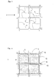
- Fig. 1 shows a wafer 7, which at the end of the Manufacturing process along horizontal and vertical Cut lines 4, 6 in a variety of square chips is divided.
- the dicing is typically called “dicing” referred to and is generally known as such.
- FIG. 2 shows a section of the wafer from FIG. 1 two identical chips or semiconductor chips 12, 22 as examples.
- the first chip 12 has a plurality of essentially rectangular or more precisely square openings 14.
- the Openings 14 are along the sides or edges of one inner square 30, the openings 14 in four groups 32, 34, 36, 38 are generated or arranged are, each of the four groups having an elongated structure forms.
- the four groups 32, 34, 36, 38 of openings each extend linearly along a straight, parallel to one of the edges of the square 30.
- an elongated, line-shaped, straight trench 40 which is also a elongated structure in the sense of the invention.
- a cover material 1 is shown, which is exemplary consists of a sheet of glass.
- the cover material 1 is as seen in Fig. 5 for rear application on a Carrier substrate 5 with several integrated, for example optical components (chips) using a so-called “Waver-Level Package Process" are produced, adjusted accordingly.
- the Chips still housed in the wafer association and the contacts after led outside.
- dashed lines 2 the breakdown lines for one after the housing and contacting, subsequent disassembly of the wafer assembly, i.e. that for the subsequent dicing of the wafer into individual Chips, and thus define the subsequent chip size.
- a mask for example by means of a screen printing process and / or applied photolithographic process.
- One here generated band structure of 100 to 200 microns has here proven sufficiently.
- the creation of the slots 3 themselves is preferably carried out by means of sandblasting, wherein especially a thin display glass, which is suitable for diverse, a specialist in this field per se known applications as a covering material particularly well suitable, due to a high removal rate as a result of abrasive process can be processed very quickly.
- the slots 3 after their structuring a width of approx. 200 to 500 ⁇ m on and a length which, as seen from Fig. 3, is somewhat is shorter than the long side of a chip, so that between individual bars remain in the slots.
- the length of a Slot is essentially determined by the stability limit of the used as cover material 1 limited.
- the formation of the slits 3 also with other suitable methods, in particular be carried out by means of an ultrasonic vibratory lapping, which leads to a higher accuracy of the Slot dimensioning leads.
- ultrasonic vibratory lapping For structuring through Ultrasonic vibratory lapping is particularly preferred Way the special procedures and devices as in the parallel at the German Patent and Trademark Office filed by the same applicant with the title "Method for creating a structure in a workpiece" are described. The content of these referenced Registration is therefore complete as part of the present Disclosure content.
- Adhesive 52 preferably an epoxy, a wax or a Sol gel applied, for example, by screen printing.
- Cover material 1 by means of bonding, in particular anodic Apply bonding to the wafer or the wafer association.
- the wafer assembly shown here comprises one for each chip Silicon layer 5 as a carrier substrate, which on the one hand Surface an optically active layer 18, such as that Includes sensor layer of a CCD chip. Furthermore, that is Silicon substrate 5 covered with a passivation layer 50 and contacting areas or so-called bond pads 16 for electrical connection of the respective chip are not about illustrated conductor tracks with the optically sensitive layer 18 connected.
- a transparent glass pane 1 ' is optical to protect it sensitive layer 18 additionally on the top of the Wafer dressing applied by means of an adhesive 52.
- the optically inactive side of the wafer dressing is the Cover 1 structured according to the invention also with Adhesives 52 attached.
- the bond pads 16 are initially via contact connections 9 through connecting channels through the carrier substrate 5 and then via the slots 3 to the rear outside led by the wafer association. Forming the Contact connections through the slots 3 will be as above preferably mentions photolithographically and / or by means of a Layer deposition produced.
- the previous structuring of the covering material 1 on V-Grooving i.e. the subsequent digging of trenches the covering material applied to the carrier substrate 5 to be dispensed with.
- the invention provides that the slots 3 if necessary. after formation of the contact connections 9, be it through Vias according to the one referred to above Patent application or by means of another of the Wafer methods known to those skilled in the art Level packaging with an insulating filling material to fill up, for example with an epoxy around a quasi-hermetic Manufacture package.
- the cover 1 'on the optically active side according to 5 can be structured beforehand with corresponding slots.
- the materials must be on the front and back Cover 1 'or 1 may not be identical. To at one Heating and / or cooling the chip has a di-metallic effect to compensate, it is already sufficient that the Stiffness of the materials, especially based on their Thickness, the respective modulus of elasticity and the Thermal expansion coefficients compensate each other to avoid bending the chip.
- a carrier substrate 5 mounted in this way with one or Several integrated components are also suitable for Production of three-dimensional integrated Circuits, in particular according to the disclosure content of equally at the German Patent and Trademark Office pending application by the same applicant under the title "Process for the production of three-dimensional structures integrated circuits and multilayer Semiconductor device "the content of which is therefore fully extensive Disclosure content of the present description belongs can be seen.
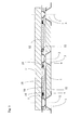
- Fig. 6 shows a sectional drawing through the two in Fig. 2 shown in the undivided wafer composite located chips 12, 22.
- the wafer 7 points at its Underside of a passivation or passivation layer 50 and is with an epoxy resin layer 52 on one Glass support 60 glued on.
- On the bottom of the wafer 7 are located within the passivation layer 50 Contact points or bond pads 16.
- the bond pads 16 are by means of Lapping through openings 14 through the wafer exposed and contactable from above.
- the first and second optical chips 12, 22 each light sensitive area, e.g. a CCD 18 or 28.
- the one with the bond pads 16 and wafers 7 provided with photosensitive regions 18, 28 glued to the glass substrate 60 by means of the epoxy resin 52. Thereafter, using the lapping process according to the invention with a lapping stamp successively or at least partially at the same time the trench 40, the first, second, third and fourth line-shaped group 32, 34, 36, 38 of openings 14 lapped into the wafer 2.
- both the openings 14, at least in one dimension, as well as the trench 40 one tapering trapezoidal cross-section.
- the openings 14 extend from a first Surface 7a of the wafer 7 up to the associated bond pads 16 on a second surface 7b of the wafer 7.
- the trench 40 extends from the first surface 7a into the Passivation layer 50.
- FIG. 7 shows a first embodiment of a Stamp or lapping stamp 70 according to the invention with a Longitudinal axis 72.
- the lapping die 70 points perpendicular to the Longitudinal axis 72 has a trapezoidal cross section 74 on and oscillates linearly along arrow 76.
- FIG. 8 shows an alternative embodiment of a Wafers 7 ', which are coated on both sides by means of epoxy layers 52', 52 '' with a first and second glass support 60 ', 60' ' a sandwich-like composite is glued on both sides.
- Trench or V-Groove 40 ' which by means of the lapping die 70 generated extends from a first surface 60a ' of the first glass carrier 60 'completely through the first Glass carrier 60 ', the first epoxy layer 52', the Silicon wafer 7 'and the second epoxy layer 52' ', so that within the trench 40 'of the silicon wafer 7' over its entire thickness is exposed.
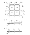
- Fig. 9 shows an alternative use of the lapping method according to the invention on a glass support 160, which is not yet connected to a wafer.
- the in Fig. 9 shown section of the glass carrier 160 divided divided into four sections 112, 122, 132 and 142, which of Boundary edges 104, 106 horizontally and vertically delimited from each other and individual chips on a wafer assigned.
- the boundary edges 104, 106 of the four square areas 112, 122, 132, 142 are respectively oblong rectangular openings 140 introduced or lapped. Between adjacent openings 140 a web 141 is left in each case, so that the Glass support 160 remains as one piece.
- the Boundary edges 104, 106 each form the longitudinal axes a linearly extending structure comprising one or more of the openings 140.
- FIG. 10 shows two of the openings 140 in one Sectional drawing along line B-B in Fig. 9, i.e. along the longitudinal axis of the openings 140.
- the openings 140 penetrate the glass carrier 160 completely from a first Surface 160a to a second surface 160b.
- Fig. 11 shows three openings 140 in a section along the Line C-C in Fig. 9, i.e. transverse or perpendicular to the longitudinal axis of the openings 140.
- the openings 140 have according to this Embodiment transverse to its longitudinal axis square cross section, but can be in others Embodiments also e.g. a trapezoidal or have triangular cross-section.
- Figures 9 to 11 are also for the sake of better Not true to scale.
- the length of the openings 140 is about 1 mm to 40 mm and the width is about 40 ⁇ m to 100 ⁇ m, 100 ⁇ m to 100 ⁇ m or 300 ⁇ m to 800 ⁇ m.
- the glass carrier 160 comprises, for example, alkali-free glass, in particular AF45 or glass of the D263 type from Schott Glas, which have an expansion coefficient of approximately 4.5 ⁇ 10 -6 , which is similar to that of silicon with 3.6 ⁇ 10 -6 .
- Fig. 12 shows a second embodiment of the Lapping punch 170 according to the invention with a head section 171 with a rectangular cross section 172 and a lower one Section 173 with a triangular cross section 174.
- the lower section 173 has material-removing sections 175, 176 and a recess 177 arranged between them.
- Two End faces 177a, 177b of the rectangular recess 177 extend parallel to each other and perpendicular to Longitudinal axis of the lapping die.
- With the lapping stamp 170 a slotted workpiece with sloping side surfaces.
- FIG. 13 shows the lapping stamp from FIG. 12 in one Side view, with a second recess 178 is shown.
- FIG. 14 shows a third embodiment of the Lapping stamp 180 according to the invention with a rectangular Cross section 182 and recesses 187, 188.
- the Lapping punch 180 With the Lapping punch 180 becomes a slotted workpiece, e.g. the slotted glass supports 160 in FIG. 9 with slotted side surfaces, which is essentially perpendicular to Surface run, created.
- 15 shows a side view of the lapping die 180.
- 16 shows a fourth embodiment of the lapping die 190 to produce a linear or elongated Structure comprising a plurality of along a straight line Holes arranged in line.
- the lapping die 190 comprises a plurality of itself tapered material-removing sections 193, 194, 195, 196 each with concave side faces and down tapered cross section 192.
- the lapping die is 190 e.g. one of the groups 32, 34, 36, 38 in one operation of openings 14, as shown in Fig. 2, can be produced.
- the openings 14 are produced in particular in groups and / or in chips, so that four per chip Lapping operations are carried out. But it is also possible to perform the creation of the openings 14, so that several along a straight line on the wafer arranged chips are simultaneously provided with openings.
- 17 shows a side view of the lapping die 190.
- the Lapping tool a plate with a two-dimensional array from needle-like tips or stamps, so that also a two-dimensional array of openings can be generated simultaneously.
Landscapes
- Processing Of Stones Or Stones Resemblance Materials (AREA)
- Mechanical Treatment Of Semiconductor (AREA)
Applications Claiming Priority (4)
| Application Number | Priority Date | Filing Date | Title |
|---|---|---|---|
| DE10141710 | 2001-08-25 | ||
| DE10141709 | 2001-08-25 | ||
| DE10141710A DE10141710A1 (de) | 2001-08-25 | 2001-08-25 | Mechanische Strukturierung von Abdeckungsmaterialien zur Verwendung in der elektrischen Aufbau- und Verbindungstechnik |
| DE10141709A DE10141709A1 (de) | 2001-08-25 | 2001-08-25 | Verfahren und Vorrichtung zum Erzeugen einer Struktur in einem Werkstück |
Publications (2)
| Publication Number | Publication Date |
|---|---|
| EP1289009A2 true EP1289009A2 (fr) | 2003-03-05 |
| EP1289009A3 EP1289009A3 (fr) | 2004-09-08 |
Family
ID=26010000
Family Applications (1)
| Application Number | Title | Priority Date | Filing Date |
|---|---|---|---|
| EP02018858A Withdrawn EP1289009A3 (fr) | 2001-08-25 | 2002-08-23 | Structuration mécanique des matériaux de recouvrement pour l'assemblage des composants électriques |
Country Status (1)
| Country | Link |
|---|---|
| EP (1) | EP1289009A3 (fr) |
Cited By (1)
| Publication number | Priority date | Publication date | Assignee | Title |
|---|---|---|---|---|
| CN112108481A (zh) * | 2019-06-21 | 2020-12-22 | 北京振兴计量测试研究所 | 一种解剖塑封光耦的方法 |
Family Cites Families (5)
| Publication number | Priority date | Publication date | Assignee | Title |
|---|---|---|---|---|
| JPS5568659A (en) * | 1978-11-20 | 1980-05-23 | Hitachi Ltd | Semiconductor device and manufacturing method thereof |
| DE4029285A1 (de) * | 1990-09-14 | 1992-03-19 | Siemens Ag | Anordnung zur ultraschallbearbeitung |
| US5965933A (en) * | 1996-05-28 | 1999-10-12 | Young; William R. | Semiconductor packaging apparatus |
| US5798557A (en) * | 1996-08-29 | 1998-08-25 | Harris Corporation | Lid wafer bond packaging and micromachining |
| IL133453A0 (en) * | 1999-12-10 | 2001-04-30 | Shellcase Ltd | Methods for producing packaged integrated circuit devices and packaged integrated circuit devices produced thereby |
-
2002
- 2002-08-23 EP EP02018858A patent/EP1289009A3/fr not_active Withdrawn
Cited By (2)
| Publication number | Priority date | Publication date | Assignee | Title |
|---|---|---|---|---|
| CN112108481A (zh) * | 2019-06-21 | 2020-12-22 | 北京振兴计量测试研究所 | 一种解剖塑封光耦的方法 |
| CN112108481B (zh) * | 2019-06-21 | 2022-05-13 | 北京振兴计量测试研究所 | 一种解剖塑封光耦的方法 |
Also Published As
| Publication number | Publication date |
|---|---|
| EP1289009A3 (fr) | 2004-09-08 |
Similar Documents
| Publication | Publication Date | Title |
|---|---|---|
| DE10031252A1 (de) | Verfahren zur Zertrennung eines Substratwafers in eine Anzahl von Substratchips | |
| EP2287916A2 (fr) | Connexion et logement des modules à circuits integrés | |
| EP1419102A2 (fr) | Procede pour la production de composants micro-electromecaniques | |
| DE69530280T2 (de) | Farbstrahldruckkopfherstellungsverfahren | |
| WO2000031796A1 (fr) | Procede de production d'un circuit integre traite sur ses deux faces | |
| EP1869705B1 (fr) | Procédé de fabrication de dispositifs électroniques en boîtier et dispositif électronique en boîtier | |
| DE10356885B4 (de) | Verfahren zum Gehäusen von Bauelementen und gehäustes Bauelement | |
| DE69715289T2 (de) | Elektrode für Plasmaätzen; Vorrichtung und Verfahren mit dieser Elektrode | |
| EP2041787A1 (fr) | Procédé d'encapsulation de composants électroniques et de circuits intégrés | |
| DE102004001892A1 (de) | FBAR-Vorrichtung vom Wafer-Level-Package-Typ und zugehöriges Herstellungsverfahren | |
| DE19707887C2 (de) | Verfahren zum Herstellen und Trennen von elektronischen Elementen mit leitfähigen Kontaktanschlüssen | |
| DE102009045541B4 (de) | Verfahren zur Herstellung einer mikromechanischen Vorrichtung | |
| DE69836813T2 (de) | Verfahren zur Herstellung von Winkelgeschwindigkeitsmessern | |
| CH684611A5 (de) | Verfahren zur Herstellung kapazitiver Sensoren und kapazitiver Sensor. | |
| DE102004001337A1 (de) | Elektrostatische Vibrationsvorrichtung | |
| DE602004010097T2 (de) | Piezoelektrische kompositmaterialien und herstellungsverfahren dafür | |
| EP1522095B1 (fr) | Procede de production d'un composant a surfaces de connexion profondes | |
| EP0774165B1 (fr) | Procede de fabrication d'un circuit tridimensionnel | |
| DE2924068A1 (de) | Verfahren zur herstellung einer koplanaren photokoppelanordnung | |
| EP1270504A1 (fr) | Dispositif à semiconducteur attaché à un wafer | |
| DE112011105215B4 (de) | Bauelementträgerverbund und Verfahren zur Herstellung einer Mehrzahl von Bauelementträgerbereichen | |
| DE19616014A1 (de) | Verfahren zur Herstellung von mikromechanische Strukturen aufweisenden Halbleiterbauelementen | |
| DE102004010703B4 (de) | Bauelement mit WLP-fähiger Verkapselung und Herstellverfahren | |
| WO2023016912A1 (fr) | Procédé de production d'une pluralité de puces laser à semi-conducteur et puce laser à semi-conducteur | |
| DE10141710A1 (de) | Mechanische Strukturierung von Abdeckungsmaterialien zur Verwendung in der elektrischen Aufbau- und Verbindungstechnik |
Legal Events
| Date | Code | Title | Description |
|---|---|---|---|
| PUAI | Public reference made under article 153(3) epc to a published international application that has entered the european phase |
Free format text: ORIGINAL CODE: 0009012 |
|
| AK | Designated contracting states |
Kind code of ref document: A2 Designated state(s): AT BE BG CH CY CZ DE DK EE ES FI FR GB GR IE IT LI LU MC NL PT SE SK TR Designated state(s): AT BE BG CH CY CZ DE DK EE ES FI FR GB GR IE IT LI LU MC NL PT SE SK TR |
|
| AX | Request for extension of the european patent |
Extension state: AL LT LV MK RO SI |
|
| PUAL | Search report despatched |
Free format text: ORIGINAL CODE: 0009013 |
|
| AK | Designated contracting states |
Kind code of ref document: A3 Designated state(s): AT BE BG CH CY CZ DE DK EE ES FI FR GB GR IE IT LI LU MC NL PT SE SK TR |
|
| AX | Request for extension of the european patent |
Extension state: AL LT LV MK RO SI |
|
| RIC1 | Information provided on ipc code assigned before grant |
Ipc: 7B 06B 3/00 B Ipc: 7H 01L 21/50 B Ipc: 7H 01L 23/10 B Ipc: 7H 01L 23/02 A |
|
| RAP1 | Party data changed (applicant data changed or rights of an application transferred) |
Owner name: SCHOTT AG |
|
| 17P | Request for examination filed |
Effective date: 20041004 |
|
| AKX | Designation fees paid |
Designated state(s): AT BE BG CH CY CZ DE DK EE ES FI FR GB GR IE IT LI LU MC NL PT SE SK TR |
|
| STAA | Information on the status of an ep patent application or granted ep patent |
Free format text: STATUS: THE APPLICATION IS DEEMED TO BE WITHDRAWN |
|
| 18D | Application deemed to be withdrawn |
Effective date: 20100302 |