EP1289083A1 - Dispositif laser DFB et module laser - Google Patents
Dispositif laser DFB et module laser Download PDFInfo
- Publication number
- EP1289083A1 EP1289083A1 EP02019212A EP02019212A EP1289083A1 EP 1289083 A1 EP1289083 A1 EP 1289083A1 EP 02019212 A EP02019212 A EP 02019212A EP 02019212 A EP02019212 A EP 02019212A EP 1289083 A1 EP1289083 A1 EP 1289083A1
- Authority
- EP
- European Patent Office
- Prior art keywords
- dfb laser
- laser device
- dfb
- laser assembly
- equal
- Prior art date
- Legal status (The legal status is an assumption and is not a legal conclusion. Google has not performed a legal analysis and makes no representation as to the accuracy of the status listed.)
- Withdrawn
Links
- 230000003287 optical effect Effects 0.000 claims description 33
- 238000002347 injection Methods 0.000 claims description 31
- 239000007924 injection Substances 0.000 claims description 31
- 239000013307 optical fiber Substances 0.000 claims description 12
- 239000004065 semiconductor Substances 0.000 claims description 8
- PMHQVHHXPFUNSP-UHFFFAOYSA-M copper(1+);methylsulfanylmethane;bromide Chemical compound Br[Cu].CSC PMHQVHHXPFUNSP-UHFFFAOYSA-M 0.000 claims description 2
- 229910003460 diamond Inorganic materials 0.000 claims description 2
- 239000010432 diamond Substances 0.000 claims description 2
- 238000002474 experimental method Methods 0.000 description 31
- 230000008859 change Effects 0.000 description 22
- 238000004891 communication Methods 0.000 description 9
- 230000007774 longterm Effects 0.000 description 9
- 229910004205 SiNX Inorganic materials 0.000 description 7
- 238000000034 method Methods 0.000 description 7
- 239000000758 substrate Substances 0.000 description 7
- 229910000530 Gallium indium arsenide Inorganic materials 0.000 description 4
- 238000002310 reflectometry Methods 0.000 description 4
- 230000008901 benefit Effects 0.000 description 3
- 230000000903 blocking effect Effects 0.000 description 3
- 230000007423 decrease Effects 0.000 description 3
- 238000010894 electron beam technology Methods 0.000 description 3
- 239000000463 material Substances 0.000 description 3
- 238000005476 soldering Methods 0.000 description 3
- 238000000429 assembly Methods 0.000 description 2
- 230000000712 assembly Effects 0.000 description 2
- 230000015556 catabolic process Effects 0.000 description 2
- 238000005253 cladding Methods 0.000 description 2
- 238000006731 degradation reaction Methods 0.000 description 2
- 238000005530 etching Methods 0.000 description 2
- 238000005259 measurement Methods 0.000 description 2
- 229910052751 metal Inorganic materials 0.000 description 2
- 239000002184 metal Substances 0.000 description 2
- 238000002488 metal-organic chemical vapour deposition Methods 0.000 description 2
- PIGFYZPCRLYGLF-UHFFFAOYSA-N Aluminum nitride Chemical compound [Al]#N PIGFYZPCRLYGLF-UHFFFAOYSA-N 0.000 description 1
- OKTJSMMVPCPJKN-UHFFFAOYSA-N Carbon Chemical compound [C] OKTJSMMVPCPJKN-UHFFFAOYSA-N 0.000 description 1
- 230000004075 alteration Effects 0.000 description 1
- 238000004458 analytical method Methods 0.000 description 1
- 230000005540 biological transmission Effects 0.000 description 1
- 229910052799 carbon Inorganic materials 0.000 description 1
- 239000000470 constituent Substances 0.000 description 1
- 238000001816 cooling Methods 0.000 description 1
- 230000008878 coupling Effects 0.000 description 1
- 238000010168 coupling process Methods 0.000 description 1
- 238000005859 coupling reaction Methods 0.000 description 1
- 230000003247 decreasing effect Effects 0.000 description 1
- 238000001312 dry etching Methods 0.000 description 1
- 230000000694 effects Effects 0.000 description 1
- 238000010438 heat treatment Methods 0.000 description 1
- 238000001459 lithography Methods 0.000 description 1
- 238000012986 modification Methods 0.000 description 1
- 230000004048 modification Effects 0.000 description 1
- 238000000623 plasma-assisted chemical vapour deposition Methods 0.000 description 1
- 230000009467 reduction Effects 0.000 description 1
- 230000001629 suppression Effects 0.000 description 1
Images



Classifications
-
- H—ELECTRICITY
- H01—ELECTRIC ELEMENTS
- H01S—DEVICES USING THE PROCESS OF LIGHT AMPLIFICATION BY STIMULATED EMISSION OF RADIATION [LASER] TO AMPLIFY OR GENERATE LIGHT; DEVICES USING STIMULATED EMISSION OF ELECTROMAGNETIC RADIATION IN WAVE RANGES OTHER THAN OPTICAL
- H01S5/00—Semiconductor lasers
- H01S5/10—Construction or shape of the optical resonator, e.g. extended or external cavity, coupled cavities, bent-guide, varying width, thickness or composition of the active region
- H01S5/12—Construction or shape of the optical resonator, e.g. extended or external cavity, coupled cavities, bent-guide, varying width, thickness or composition of the active region the resonator having a periodic structure, e.g. in distributed feedback [DFB] lasers
-
- H—ELECTRICITY
- H01—ELECTRIC ELEMENTS
- H01S—DEVICES USING THE PROCESS OF LIGHT AMPLIFICATION BY STIMULATED EMISSION OF RADIATION [LASER] TO AMPLIFY OR GENERATE LIGHT; DEVICES USING STIMULATED EMISSION OF ELECTROMAGNETIC RADIATION IN WAVE RANGES OTHER THAN OPTICAL
- H01S5/00—Semiconductor lasers
- H01S5/02—Structural details or components not essential to laser action
- H01S5/022—Mountings; Housings
- H01S5/0225—Out-coupling of light
- H01S5/02251—Out-coupling of light using optical fibres
-
- H—ELECTRICITY
- H01—ELECTRIC ELEMENTS
- H01S—DEVICES USING THE PROCESS OF LIGHT AMPLIFICATION BY STIMULATED EMISSION OF RADIATION [LASER] TO AMPLIFY OR GENERATE LIGHT; DEVICES USING STIMULATED EMISSION OF ELECTROMAGNETIC RADIATION IN WAVE RANGES OTHER THAN OPTICAL
- H01S5/00—Semiconductor lasers
- H01S5/02—Structural details or components not essential to laser action
- H01S5/022—Mountings; Housings
- H01S5/0233—Mounting configuration of laser chips
- H01S5/0234—Up-side down mountings, e.g. Flip-chip, epi-side down mountings or junction down mountings
-
- H—ELECTRICITY
- H01—ELECTRIC ELEMENTS
- H01S—DEVICES USING THE PROCESS OF LIGHT AMPLIFICATION BY STIMULATED EMISSION OF RADIATION [LASER] TO AMPLIFY OR GENERATE LIGHT; DEVICES USING STIMULATED EMISSION OF ELECTROMAGNETIC RADIATION IN WAVE RANGES OTHER THAN OPTICAL
- H01S5/00—Semiconductor lasers
- H01S5/02—Structural details or components not essential to laser action
- H01S5/024—Arrangements for thermal management
- H01S5/02407—Active cooling, e.g. the laser temperature is controlled by a thermo-electric cooler or water cooling
- H01S5/02415—Active cooling, e.g. the laser temperature is controlled by a thermo-electric cooler or water cooling by using a thermo-electric cooler [TEC], e.g. Peltier element
-
- H—ELECTRICITY
- H01—ELECTRIC ELEMENTS
- H01S—DEVICES USING THE PROCESS OF LIGHT AMPLIFICATION BY STIMULATED EMISSION OF RADIATION [LASER] TO AMPLIFY OR GENERATE LIGHT; DEVICES USING STIMULATED EMISSION OF ELECTROMAGNETIC RADIATION IN WAVE RANGES OTHER THAN OPTICAL
- H01S5/00—Semiconductor lasers
- H01S5/06—Arrangements for controlling the laser output parameters, e.g. by operating on the active medium
- H01S5/068—Stabilisation of laser output parameters
-
- H—ELECTRICITY
- H01—ELECTRIC ELEMENTS
- H01S—DEVICES USING THE PROCESS OF LIGHT AMPLIFICATION BY STIMULATED EMISSION OF RADIATION [LASER] TO AMPLIFY OR GENERATE LIGHT; DEVICES USING STIMULATED EMISSION OF ELECTROMAGNETIC RADIATION IN WAVE RANGES OTHER THAN OPTICAL
- H01S5/00—Semiconductor lasers
- H01S5/20—Structure or shape of the semiconductor body to guide the optical wave ; Confining structures perpendicular to the optical axis, e.g. index or gain guiding, stripe geometry, broad area lasers, gain tailoring, transverse or lateral reflectors, special cladding structures, MQW barrier reflection layers
- H01S5/22—Structure or shape of the semiconductor body to guide the optical wave ; Confining structures perpendicular to the optical axis, e.g. index or gain guiding, stripe geometry, broad area lasers, gain tailoring, transverse or lateral reflectors, special cladding structures, MQW barrier reflection layers having a ridge or stripe structure
- H01S5/227—Buried mesa structure ; Striped active layer
- H01S5/2275—Buried mesa structure ; Striped active layer mesa created by etching
Definitions
- the present invention relates to a distributed feedback semiconductor laser assembly (DFB laser assembly) including a DFB laser device and a heat sink onto which the DFB laser device is bonded. More specifically, the present invention relates to a DFB laser assembly having a high degree of wavelength stability, having a smaller range of variation in the emission wavelength with respect to a change in the operating current, and is thus suited to act as a light source for use in an optical communications system. The present invention also relates to a DFB laser module having such a DFB laser assembly.
- DFB laser assembly distributed feedback semiconductor laser assembly
- a DFB laser device has in its resonant cavity a diffraction grating for periodically changing the real part and/or the imaginary part of the refractive index (complex refractive index) in the resonant cavity so that only laser light having a specific wavelength is fed-back to the resonant cavity for wavelength selectivity.
- a DFB laser device diffraction grating has a plurality of stripe layers disposed adjacent to the active layer. The stripe layers may be periodically arranged and may have a refractive index different from the refractive index of the adjacent layer in the resonant cavity.
- This configuration allows the DFB laser device to select an emission wavelength ⁇ DFB independently of the optical gain peak wavelength of the active layer.
- a typical DFB laser device is considered to be a promising light source for use in a long-distance optical communications system.
- a DFB laser device incorporated in a butterfly type DFB laser module is commonly used as a light source in the long-distance optical communications system.
- the DFB laser module 60 is configured to have 14 pins and emits a laser beam via an optical fiber 68.
- the DFB laser module 60 includes a DFB laser device 52, a heat sink 54, and a thermistor 56.
- the DFB laser device 52 is bonded onto the heat sink 54 made of aluminum nitride (AlN), which is supported on a base 72 and acts to dissipate the heat energy generated in the DFB laser device 52.
- the thermistor 56 is also provided on the heat sink 54 and serves to measure the operating temperature of the DFB laser device 52.
- the DFB laser module 60 is generally driven to generate a constant optical output power in an APC (Auto Power Control) mode when employed as a light source in an optical communications system. Accordingly, there is provided a monitor photodiode 71 for detecting the optical output power from the DFB laser device 52 and for delivering a control signal to generate a constant optical output power.
- the monitor photodiode 71 is disposed on the DFB laser side in a monitor photodiode block 70, which is provided on the base 72.
- an external feedback circuit (not shown) for adjusting the current I m delivered from the monitor photodiode 71 at a constant value in order to control a drive current and thereby emit a laser beam at a constant optical output power.
- the first lens 62 is a collimator lens which collimates the laser beam emitted from the DFB laser device 52 to allow the resulting beam to impinge upon the optical isolator 64.
- the optical isolator 64 is an optical component which prevents the reflected beam from entering through the optical fiber 68 and transmits only the laser beam incident from the first lens 62 toward the second lens 66.
- the second lens 66 collects the laser beam incident from the optical isolator 64 and then transmits the resulting beam toward the optical fiber 68.
- a Peltier element 74 beneath the base 72 to cool down or heat up the base 72.
- the Peltier element 74 cools down or heats up the DFB laser device 52 via the base 72 and the heat sink 54 to maintain the operating temperature of the DFB laser device 52, which is measured by the thermistor 56, at a predetermined temperature.
- These components including the DFB laser device 52 are received in a package 76, where a laser beam emitted from the DFB laser device 52 advances through the first lens 62, the optical isolator 64, and the second lens 66 into the optical fiber 68, which is inserted through the side-wall of the package 76, and then propagates outwardly therethrough.
- the DFB laser module 60 described above and incorporating therein the DFB laser device 52 is widely used as a signal light source in an optical communications system employing the wavelength division multiplexing scheme (or a WDM system) which enables a large-capacity transmission.
- the WDM system requires semiconductor laser devices employed as the light sources, typically DFB laser devices, to provide the strict accuracy of the emission wavelengths and thus a high degree of stability of the emission wavelengths for a long period of time.
- the tolerance of the wavelength accuracy and emission wavelength stability depend on the scale of the WDM system and the wavelengths of the laser beams of the light sources. In general, a narrower step frequency or spacing between the adjacent frequencies of the DFB laser devices requires a smaller tolerance. Approximately, the wavelength accuracy and emission wavelength stability are desired to be less than ⁇ 0.2nm for a 100GHz spacing (at a wavelength interval of up to 0.8nm) and about ⁇ 0,1nm for a 50GHz spacing (at a wavelength interval of up to 0.4nm).
- the lasing efficiency of the laser device may gradually degrade or the threshold current of the laser device may increase more or less after a long-term operation.
- a degradation in the lasing efficiency or an increase in the threshold current of the DFB laser device causes the feedback loop to increase the drive current in order to maintain the optical output power at a constant.
- such a change in the drive current causes the emission wavelength to vary significantly, thereby making it difficult to maintain the wavelength accuracy and stability required by the WDM system. Accordingly, as discovered by the present inventors, there is a need for a DFB laser device which provides a reduced range of variation in the emission wavelength thereof with respect to a change in the operating current, thereby providing a high degree of stability in the emission wavelength.
- the present invention provides, in a first aspect thereof, a distributed feedback semiconductor laser assembly (DFB laser assembly) including a DFB laser device and a heat sink mounting thereon the DFB laser device, wherein a ratio of a variation in an emission wavelength of the DFB laser device to a variation in an injection current of the DFB laser device is 5pm/mA or less, 4pm/mA or less, 3pm/mA or less, or 2pm/mA or less.
- DFB laser assembly distributed feedback semiconductor laser assembly
- the present invention also provides, in a second aspect thereof, a DFB laser module including the DFB laser assembly as described above.
- the smaller emission wavelength/injection current coefficient suppresses the range of variation in the emission wavelength of the DFB laser device, whereby the DFB laser device has a higher wavelength stability after a long-term operation or a higher output power operation.
- Fig. 1 is a sectional view illustrating the configuration of a butterfly-type DFB laser module for use in an optical communications system
- Fig. 2 is a partially cutout perspective view illustrating the configuration of a DFB laser device used as a sample of experiments 1 and 2 according to an embodiment of the present invention
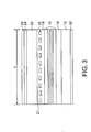
- Fig. 3 is a sectional view of the DFB laser device of Fig. 2 as viewed in the direction of arrows III-III in Fig. 2;
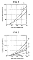
- Fig. 4 is a graph showing the measured results of the relationship between the injection current and the amount of shift in the emission wavelength in the experiments 1 and 2;
- Fig. 5 is a graph showing the measured results of the relationship between the injection current and the amount of shift in the emission wavelength in experiments 2 to 5;
- Fig. 6 is a top plan view illustrating the configuration of a DFB laser assembly according to an embodiment of the present invention.
- the term “DFB laser assembly” as used hereinafter includes at least a DFB laser device and a heat sink.
- the term “DFB laser module” as used hereinafter has the DFB laser assembly and an optical system for optically coupling the DFB laser assembly to an optical fiber.
- the inventor recognized that a variation in the emission wavelength associated with a change in the injection current (or operating current) is due to the fact that changes in the injection current cause a change in the heat generated in the DFB laser device and, therefore, the temperature of the active layer. More specifically, an increase in temperature increases the effective refractive index n eff in the resonant cavity of the DFB laser device, which causes a change in wavelength output, based on this assumption, the inventor conducted experiments and analyses and eventually reached the following findings.
- ⁇ ⁇ 0 + ⁇ ⁇ T LD - R th ( V f I f - P 0 ) ⁇ ⁇ 0 + ⁇ ⁇ T LD R th [ ⁇ V th + R ( I f - I th ) ⁇ I f -P 0 ]
- ⁇ / ⁇ T LD the emission wavelength/temperature coefficient, which determines the temperature dependency of the emission wavelength
- V f is the forward-bias voltage of the DFB laser
- V th is the forward threshold voltage of the DFB laser
- I th is the threshold current of the DFB laser device
- R th is the thermal resistance of the DFB laser device being bonded onto the heat sink
- R is the differential resistance of the DFB laser device
- P the differential resistance of the DFB laser device
- the second term on the right side or ( ⁇ / ⁇ T LD )R th [ ⁇ V th +R(I f -I th ) ⁇ I f -P 0 ], represents the emission wavelength dependency of the current.
- the ( ⁇ / ⁇ T LD ) and V th in the second term on the right side of the formula corresponds to the semiconductor materials that constitute the DFB laser device and are therefore constant relative to the emission wavelength dependency on the current. Accordingly, the present inventor recognized that the thermal resistance R th and the differential resistance R are responsible for the reduction in the emission current dependency of the emission wavelength, and therefore may be reduced to reduce the current dependency of the emission wavelength in the DFB laser device.
- the thermal resistance R th is defined as the ratio of an increase in temperature of the active layer to the power injected into the semiconductor laser and then converted into heat.
- the differential resistance R is defined as the resistance obtained by differentiating the voltage V with respect to the current I in the V-I characteristics of the DFB laser device.
- the inventor focused attention on the cavity length of the DFB laser device that defines the contact area between the DFB laser device and the heat sink, and the structure for bonding the DFB laser device onto the heat sink and defining the thermal contact resistance.
- the term "junction-up” means bonding the n-side electrode 32 of the DFB laser device 10 onto the heat sink 54 with the p-side electrode 30 thereof being directed upward
- the term “junction-down” means bonding the p-side electrode 30 of the DFB laser device 10 onto the heat sink 54 with the n-side electrode 32 thereof being directed upward.
- the DFB laser device 10 is a buried heterostructure DFB laser device having an emission wavelength of approximately 1550 nm. As shown in Fig. 2 and Fig. 3, the DFB laser device 10 has an n-InP substrate 12 on which a layer structure is formed, the layer structure including an n-InP buffer layer 14, a MQW-SCH layer 16, a p-InP spacer layer 18, a diffraction grating 20 having a space period of about 240nm, and a p-InP embedding layer 21 for embedding the diffraction grating 20.
- the p-InP spacer layer 18 receiving therein the diffraction grating 20, the MQW-SCH layer 16, and an upper portion of the n-InP buffer layer 14 are configured to form a mesa stripe.
- a p-InP layer 26 and an n-InP layer 28 are provided to form a current blocking p-n junction structure.
- the mesa stripe is about 1.5 ⁇ m wide at the depth of the MQW-SCH layer 16.
- an about-2 ⁇ m-thick p-InP cladding layer 22 and a heavily doped GaInAs contact layer 24 are consecutively deposited.
- a Ti/Pt/Au multilayer metal film is formed as a p-side electrode 30 on top of the doped GaInAs contact layer 24, whereas an AuGeNi film is formed as an n-side electrode 32 on the bottom surface of the n-InP substrate 12.
- the emitting face of the laser device is coated with an anti-reflection coat having a reflectivity of about 1%
- the rear face of the laser device is coated with a high-reflection coat having a reflectivity of about 90%.
- the reflectivity of the emitting face may be reduced down to about 3% or less, thereby making it possible to prevent the Fabry-Perot lasing mode at the peak wavelength of the optical gain distribution in the active layer.
- this may be combined with the rear face having a high reflectivity of 80% or more, thereby making it possible to increase the output efficiency from the emitting face.
- the layer structure including the n-InP buffer layer 14, the MQW-SCH layer 16, the p-InP spacer layer 18, and a diffraction grating layer are first epitaxially grown on the n-InP substrate 12 at a growth temperature of 600°C using a MOCVD system.
- the diffraction grating layer is then coated with an electron beam (EB) resistance film in a thickness of about 100nm.
- EB electron beam
- a diffraction grating pattern having a space period of about 240nm is formed on this film using an EB lithography system.
- the diffraction grating layer is selectively etched to form the diffraction grating 20.
- the p-InP embedding layer 21 is grown on the diffraction grating 20 so as to embed the diffraction grating 20.
- a SiNx film is then deposited on the entire surface of the wafer in a plasma-enhanced CVD system, followed by etching the SiNx film to form a stripe SiNx mask by a photolithographic and RIE technique, the stripe SiNx mask extending along the diffraction grating 20.
- the p-InP embedding layer 21, the diffraction grating 20, the p-InP spacer layer 18, the MQW-SCH layer 16, the n-InP buffer layer 14, and the upper portion of the n-InP substrate 12 are etched to form a mesa stripe having a width of about 1.5 ⁇ m at the depth of the MQW-SCH layer 16.
- the p-InP layer 26 and the n-InP layer 28 are consecutively grown on both sides of the mesa stripe by a selective area growth technique using the stripe SiNx mask as a selective growth blocking mask, to form a current blocking structure having a p-n junction.
- the stripe SiNx mask After removing the stripe SiNx mask, the about-2 ⁇ m-thick p-InP cladding layer 22 and the heavily doped GaInAs layer 24 are consecutively grown.
- the bottom surface of the n-InP substrate 12 is polished to allow the n-InP substrate 12 to have a thickness of about 120 ⁇ m.
- a Ti/Pt/Au multi-layer metal film is formed as the p-side electrode 30, whereas an AuGeNi film is formed as the n-side electrode 32 on the bottom surface of the n-InP substrate 12.
- the emitting facet of the DFB laser device 10 is coated with a non-reflection coat, and the rear facet thereof is coated with a high-reflection coat.
- the DFB laser device 10 fabricated as described above revealed a threshold current of about 10mA in operation.
- the DFB laser device 10 maintained a satisfactory single mode lasing with a side mode suppression ratio of 45 to 50dB.
- the following exemplary experiments 1 to 6 employed DFB laser modules similar to that shown in Figure 1, with the cavity length of the laser device changed and/or the method of bonding the laser device to the heat sink changed.
- a soldering technique was employed for the bonding the laser device 10 to the heat sink 54.
- differential resistance and thermal resistance were determined. The differential resistance was determined by measuring the V-I characteristics of the DFB laser device 10 to differentiate the voltage V with respect to the current I.
- the thermal resistance R th was determined by measuring the dependency of the emission wavelength on the injection current, then fitting the resulting measurements to the equation 1 described above.
- the operating temperature of the DFB laser device 10 is measured by the resistance of a thermistor in a configuration similar to thermistor 56 in Fig. 1. To allow this measurement, the thermistor 56 is located in close proximity to the DFB laser device 10 so as to be able to measure the operating temperature of the DFB laser device 10 (52) as accurately as possible. In the experiments 1 to 6, the distance between the DFB laser device 10 and the thermistor 56 is set within 2mm on the heat sink 54.
- junction-up or -down structure is directed to the structure of the DFB laser device being bonded onto a heat sink.
- a DFB laser module having a configuration similar to that of the DFB laser module 60 shown in Fig. 1 is used, wherein the DFB laser device 10 is bonded onto the heat sink 54 in a junction-up configuration.
- the DFB laser device 10 used in this experiment had a cavity length of 300 ⁇ m.
- the sample DFB laser device 10 having the cavity length of 300 ⁇ m had a differential resistance of 5 ⁇ .
- the thermal resistance was 80K/W for the DFB laser device 10 being bonded onto the heat sink 54 in a junction-up configuration.
- the emission wavelength/injection current coefficient is 10pm/mA at an injection current of 100mA.
- the wavelength/current coefficient at an injection current of 100mA means the ratio of the change in emission wavelength to the change in the injection current at an injection current of 100mA, that is, the ratio defined by ⁇ / ⁇ I f (pm/mA). It may be said that a smaller such coefficient provides a smaller variation of the emission wavelength in association with a change in the drive current.
- the DFB laser device 10 similar to that used in experiment 1, but bonded onto the heat sink 54 in a junction-down structure.
- This configuration revealed a thermal resistance of 55K/W.
- the relationship between the injection current and the amount of shift in the emission wavelength was measured to obtain the results as shown in graph (2) of Fig. 4.
- the wavelength/current coefficient is 7pm/mA at an injection current of 100mA.
- the thermal resistance provided by the laser assembly that is junction-down bonded is reduced to about 70% of that provided by the laser assembly that is junction-up bonded, whereby the wavelength/current coefficient is reduced down to 70% in the junction-down bonding.
- the DFB laser device having a cavity length of 400 ⁇ m was employed as a sample DFB laser device.
- the sample DFB laser device 10 had a differential resistance of 4 ⁇ .
- the thermal resistance was 50K/W for the DFB laser device 10 being bonded onto the heat sink 54 in a junction-down structure.
- the wavelength/current coefficient is 5pm/mA at an injection current of 100mA, for example.
- the DFB laser device having a cavity length of 500 ⁇ m was employed as a sample DFB laser.
- the sample DFB laser device 10 had a differential resistance of 3.5 ⁇ .
- the thermal resistance was 45K/W for the DFB laser device 10 being bonded onto the heat sink 54 in a junction-down structure.
- the wavelength/current coefficient was 4pm/mA at an injection current of 100mA, for example.
- the DFB laser device having a cavity length of 600 ⁇ m was employed as a sample DFB laser device.
- the sample DFB laser device 10 had a differential resistance of 3 ⁇ .
- the thermal resistance was 40K/W for the DFB laser device 10 being bonded onto the heat sink 54 in a junction-down structure.
- the wavelength/current coefficient is 3pm/mA at an injection current of 100mA, for example.
- the DFB laser device having a cavity length of 800 ⁇ m was employed as a sample DFB laser device.
- the sample DFB laser device 10 had a differential resistance of 2 ⁇ .
- the thermal resistance was 30K/W for the DFB laser device 10 being bonded onto the heat sink 54 in a junction-down structure.
- the wavelength/current coefficient is 2pm/mA at an injection current of 100mA, for example.
- a larger cavity length reduces the variation in the emission wavelength caused by a change in the injection current. This is because the larger cavity length of the DFB laser device reduces the differential resistance of the DFB laser device and also reduces the thermal resistance between the DFB laser device and the heat sink.
- junction down bonding a relatively long cavity laser device provides the unexpected advantage of a small wavelength change per unit change of drive current.
- the inventor also observed that a smaller variation in the drive current also reduces the variation in the emission wavelength.
- a smaller value of the drive current reduces the variation itself in the drive current and thus reduces the variation in the emission wavelength. This means that using the same DFB lasers at a lower drive current or at a lower optical output power provides less variation in the emission wavelength for a specified percent increase in the drive current.
- the reduced wavelength/current coefficient can provide a significantly smaller variation in the emission wavelength.
- the present invention provides a DFB laser assembly including: a DFB laser having a cavity length of 400 ⁇ m or more and a differential resistance of 4 ⁇ or lower; and a heat sink to which the DFB laser is bonded in a junction-down structure to provide a thermal resistance of 50K/W or less.
- the DFB laser has a feature that a ratio of a change in emission wavelength to a change in injection current of the operating current in operation is 5pm/mA or less.
- the DFB laser device has a cavity length of 500 ⁇ m or more and a differential resistance of 3.5 ⁇ or lower, and is bonded onto the heat sink in a junction-down structure to have a thermal resistance of 45K/W or less. This makes the rate of change in the emission wavelength at 4pm/mA or less in the DFB laser device.
- the DFB laser has a cavity length of 600 ⁇ m or more and a differential resistance of 3 ⁇ or lower, and is bonded onto the heat sink in a junction-down structure to have a thermal resistance of 40K/W or less. This makes the rate of change in emission wavelength at 3pm/mA or less.
- the DFB laser has a cavity length of 800 ⁇ m or more and a differential resistance of 2 ⁇ or lower, and is bonded onto the heat sink in a junction-down structure to have a thermal resistance of 30K/W or less. This makes the rate of change in emission wavelength at 2pm/mA or less.
- the bonding structure employs, but not limited to, soldering as long as it provides a thermal resistance of a specific value or less.
- the heat sink is preferably made of a material having a high thermal conductivity and a thermal expansion coefficient close to that of the constituent materials of the semiconductor laser device, such as aluminum nitride, diamond, or diamond-like carbon.
- the present invention also provides a DFB laser module including: a DFB laser assembly having a DFB laser device and a heat sink bonded onto the DFB laser device, for dissipating heat energy generated in the DFB laser device; a temperature measuring device, disposed in close proximity to the DFB laser on the heat sink, for measuring the operating temperature of the DFB laser device; and a Peltier element for cooling down or heating up the DFB laser device via the heat sink to maintain the operating temperature of the DFB laser device measured by the temperature measuring device at a predetermined temperature.
- the DFB laser module has a feature that the DFB laser assembly is the DFB laser assembly described above and is configured to deliver a constant optical output.
- the wavelength/current coefficient is defined to have a specific value or less, the variation in the emission wavelength is significantly smaller even when the lasing efficiency has decreased or the threshold current has increased after a long-term service of the DFB laser assembly and module.
- a DFB laser assembly 50 of the present embodiment includes a buried heterostructure DFB laser device 52 having a cavity length of 400 ⁇ m and a differential resistance of 4 ⁇ .
- the DFB laser assembly 50 further includes a heat sink 54 onto which the DFB laser device 52 is bonded by a soldering technique in a junction-down structure to have a thermal resistance of 50K/W or less.
- a thermistor 56 is also provided to measure the operating temperature of the DFB laser device 52.
- the DFB laser device 52 has a configuration similar to that of the DFB laser device 10 used as a sample in the exemplary experiments 1 to 6 as described before.
- the DFB laser assembly 50 of the present embodiment provides a wavelength/current coefficient of 5pm/mA at an operating current of 100mA, the wavelength/current coefficient being defined by the ratio of the change in the emission wavelength to the variation in injection current causing the change in the emission wavelength.
- the DFB laser assembly 50 of the present embodiment has a lower wavelength/current coefficient, the variation in the emission wavelength is significantly smaller even when the lasing efficiency decreases or the threshold current increases after a long-term service of the DFB laser assembly 50.
- the DFB laser assembly 50 has an advantage of providing less variation in the emission wavelength compared with the conventional DFB laser assembly, particularly during operating at a high output power.
- the DFB laser assembly of the second embodiment has a configuration similar to that of the first embodiment except that the cavity length is 500 ⁇ m, the differential resistance is 3.5 ⁇ , and the thermal resistance is 45K/W or less in the second embodiment.
- the second embodiment provides a wavelength/current coefficient of 4pm/mA at an operating current of 100mA.
- the DFB laser assembly of the third embodiment has a configuration similar to that of the first embodiment except that the cavity length is 600 ⁇ m, the differential resistance is 3 ⁇ , and the thermal resistance is 40K/W or less in the third embodiment.
- the third embodiment provides a wavelength/current coefficient of 3pm/mA at an operating current of 100mA.
- the DFB laser assembly of the second and third embodiments provide further reduced wavelength/current coefficients compared to the DFB laser assembly of the first embodiment. Accordingly, each of the DFB laser assemblies of these embodiments provides a further reduced variation in the emission wavelength and a higher degree of wavelength stability even when the lasing efficiency decreases or the threshold current increases after a long-term service of the DFB laser assembly. In addition, each DFB laser assembly provides less variation in the emission wavelength during operating at a high output power, thereby providing a higher degree of wavelength stability.
- the DFB laser module of the fourth embodiment has a configuration similar to that of the DFB laser module 60 shown in Fig. 2 except that the DFB laser module of the present embodiment employs any one of the DFB laser assemblies according to the first through third embodiments as a DFB laser assembly including a DFB laser device and a heat sink.
- the distance between the DFB laser device 52 and the thermistor 56 is within 2mm.
- the DFB laser module of the fourth embodiment employs, as a light source, a DFB laser assembly having a reduced wavelength/current coefficient. Accordingly, the variation in the emission wavelength is significantly smaller even when the lasing efficiency decreases or the threshold current increases after a long-term service of the DFB laser device. This allows the DFB laser assembly module to be suited for use as a light source in an optical communications system.
- a DFB laser device having a resonant cavity is bonded onto a heat sink in a junction-down structure to reduce the thermal resistance.
- This makes it possible to implement a DFB laser assembly that has a reduced variation in the emission wavelength with respect to a change in the operating current and less dependency of the emission wavelength on the operating current.
- This also makes it possible to provide a DFB laser module that is suited for a light source in an optical communications system.
- the effects of the present invention become more apparent in a laser assembly operating at a high operating current or a high output power.
- the present invention is also applicable to a DFB laser module having a so-called wavelength locker function, which is used in optical communication systems requiring an extremely high degree of wavelength stability.
Landscapes
- Physics & Mathematics (AREA)
- Condensed Matter Physics & Semiconductors (AREA)
- General Physics & Mathematics (AREA)
- Electromagnetism (AREA)
- Optics & Photonics (AREA)
- Semiconductor Lasers (AREA)
Applications Claiming Priority (4)
| Application Number | Priority Date | Filing Date | Title |
|---|---|---|---|
| JP2001257473 | 2001-08-28 | ||
| JP2001257473 | 2001-08-28 | ||
| JP2002049027 | 2002-02-26 | ||
| JP2002049027 | 2002-02-26 |
Publications (1)
| Publication Number | Publication Date |
|---|---|
| EP1289083A1 true EP1289083A1 (fr) | 2003-03-05 |
Family
ID=26621102
Family Applications (1)
| Application Number | Title | Priority Date | Filing Date |
|---|---|---|---|
| EP02019212A Withdrawn EP1289083A1 (fr) | 2001-08-28 | 2002-08-27 | Dispositif laser DFB et module laser |
Country Status (2)
| Country | Link |
|---|---|
| US (1) | US7453100B2 (fr) |
| EP (1) | EP1289083A1 (fr) |
Families Citing this family (5)
| Publication number | Priority date | Publication date | Assignee | Title |
|---|---|---|---|---|
| US20040190580A1 (en) * | 2003-03-04 | 2004-09-30 | Bardia Pezeshki | High-yield high-precision distributed feedback laser based on an array |
| US9410903B2 (en) | 2011-10-12 | 2016-08-09 | Baker Hughes Incorporated | Incoherent reflectometry utilizing chaotic excitation of light sources |
| US8681322B2 (en) | 2011-10-12 | 2014-03-25 | Baker Hughes Incorporated | Distance measurement using incoherent optical reflectometry |
| US9165591B2 (en) | 2013-08-07 | 2015-10-20 | Seagate Technology Llc | Grating based laser and power monitor for a heat-assisted magnetic recording device |
| CN109742140B (zh) * | 2018-11-23 | 2020-10-27 | 厦门市三安集成电路有限公司 | 具有单边渐变多量子阱的高阻氮化镓基缓冲层及制备方法 |
Citations (4)
| Publication number | Priority date | Publication date | Assignee | Title |
|---|---|---|---|---|
| US4360965A (en) * | 1978-12-01 | 1982-11-30 | Fujitsu Limited | Method of mounting a semiconductor laser device |
| EP0920095A2 (fr) * | 1997-11-27 | 1999-06-02 | Hitachi, Ltd. | Dispositif de contrÔle de la stabilité des longueurs d'ondes optiques et transmetteur optique |
| EP1089407A1 (fr) * | 1999-09-30 | 2001-04-04 | The Furukawa Electric Co., Ltd. | Laser à semi-conducteur à rétroaction répartie et à couplage de gain |
| US6252726B1 (en) * | 1999-09-02 | 2001-06-26 | Lightlogic, Inc. | Dual-enclosure optoelectronic packages |
Family Cites Families (8)
| Publication number | Priority date | Publication date | Assignee | Title |
|---|---|---|---|---|
| US4199888A (en) * | 1978-04-13 | 1980-04-29 | Barnes Gary D | Combined sinker and fishing lure |
| US4942689A (en) * | 1988-07-05 | 1990-07-24 | Dylist, Inc. | Fishing weight |
| US5648121A (en) * | 1993-07-01 | 1997-07-15 | Cornell, Jr.; Thomas W. | Fishing weight |
| GB9318437D0 (en) * | 1993-09-06 | 1993-10-20 | Gardner John Christopher | High specific gravity material |
| US5537775A (en) * | 1995-02-27 | 1996-07-23 | Crumrine; Douglas L. | Weighted jig hook apparatus |
| AUPO221796A0 (en) * | 1996-09-09 | 1996-10-03 | Acworth, Arthur Keith | Improvements to weights and sinkers |
| US5953848A (en) * | 1997-08-14 | 1999-09-21 | Darnell; Charles | Environmentally friendly fishing lure construction |
| JP2002064244A (ja) * | 2000-06-06 | 2002-02-28 | Furukawa Electric Co Ltd:The | 分布帰還型半導体レーザ素子 |
-
2002
- 2002-08-27 US US10/228,136 patent/US7453100B2/en not_active Expired - Lifetime
- 2002-08-27 EP EP02019212A patent/EP1289083A1/fr not_active Withdrawn
Patent Citations (4)
| Publication number | Priority date | Publication date | Assignee | Title |
|---|---|---|---|---|
| US4360965A (en) * | 1978-12-01 | 1982-11-30 | Fujitsu Limited | Method of mounting a semiconductor laser device |
| EP0920095A2 (fr) * | 1997-11-27 | 1999-06-02 | Hitachi, Ltd. | Dispositif de contrÔle de la stabilité des longueurs d'ondes optiques et transmetteur optique |
| US6252726B1 (en) * | 1999-09-02 | 2001-06-26 | Lightlogic, Inc. | Dual-enclosure optoelectronic packages |
| EP1089407A1 (fr) * | 1999-09-30 | 2001-04-04 | The Furukawa Electric Co., Ltd. | Laser à semi-conducteur à rétroaction répartie et à couplage de gain |
Non-Patent Citations (6)
| Title |
|---|
| CHEN T R ET AL: "DFB laser with 95 mW output at 1.55 mu m", PROCEEDINGS OF THE 1996 CONFERENCE ON LASERS AND ELECTRO-OPTICS, CLEO'96;ANAHEIM, CA, USA JUN 2-7 1996, 1996, Conf Proc Laser Electr Optic Soc Annu Meet;Conference Proceedings - Lasers and Electro-Optics Society Annual Meeting 1996 IEEE, Piscataway, NJ, USA, pages 336 - 337, XP002220638 * |
| JOYCE W B ET AL: "THERMAL RESISTANCE OF HETEROSTRUCTURE LASERS", JOURNAL OF APPLIED PHYSICS, AMERICAN INSTITUTE OF PHYSICS. NEW YORK, US, vol. 46, no. 2, 1 February 1975 (1975-02-01), pages 855 - 862, XP002008082, ISSN: 0021-8979 * |
| MARTINELLI R U ET AL: "1.95- M STRAINED INGAAS-INGAASP-INP DISTRIBUTED-FEEDBACK QUANTUM-WELL LASERS", IEEE PHOTONICS TECHNOLOGY LETTERS, IEEE INC. NEW YORK, US, vol. 6, no. 12, 1 December 1994 (1994-12-01), pages 1415 - 1417, XP000486220, ISSN: 1041-1135 * |
| MENNA R ET AL: "High power 1550 nm distributed feedback lasers with 440 mW CW output power for telecommunication applications", CONFERENCE ON LASERS AND ELECTRO-OPTICS (CLEO);BALTIMORE, MD, UNITED STATES MAY 6-11 2001, 2001, Conf Lasers Electro Opt Eur Tech Dig;Conference on Lasers and Electro-Optics Europe - Technical Digest 2001, pages xxiii - xxiv, XP002220637 * |
| SIMMONS J G ET AL: "Series resistance and its effect on the maximum output power of 1.5 /spl mu/m strained-layer multiple-quantum-well ridge waveguide InGaAsP lasers", OPTOELECTRONIC AND MICROELECTRONIC MATERIALS DEVICES, 1998. PROCEEDINGS. 1998 CONFERENCE ON PERTH, WA, AUSTRALIA 14-16 DEC. 1998, PISCATAWAY, NJ, USA,IEEE, US, 14 December 1998 (1998-12-14), pages 120 - 123, XP010350051, ISBN: 0-7803-4513-4 * |
| STEVENTON A G ET AL: "CW OPERATION OF GAINASP STRIPE LASERS", IEEE JOURNAL OF QUANTUM ELECTRONICS, IEEE INC. NEW YORK, US, vol. QE-17, no. 5, 1 May 1981 (1981-05-01), pages 602 - 610, XP000705541, ISSN: 0018-9197 * |
Also Published As
| Publication number | Publication date |
|---|---|
| US20030063648A1 (en) | 2003-04-03 |
| US7453100B2 (en) | 2008-11-18 |
Similar Documents
| Publication | Publication Date | Title |
|---|---|---|
| US4914667A (en) | Hybrid laser for optical communications, and transmitter, system, and method | |
| US6580740B2 (en) | Semiconductor laser device having selective absorption qualities | |
| EP1841023B1 (fr) | La température reglant la longueur d'onde d'une diode de laser par le chauffage | |
| US8155161B2 (en) | Semiconductor laser | |
| US20100074291A1 (en) | Distributed Feedback Semiconductor Laser Device | |
| US20050018732A1 (en) | Uncooled and high temperature long reach transmitters, and high power short reach transmitters | |
| JP2001339118A (ja) | 発光モジュール | |
| US6301279B1 (en) | Semiconductor diode lasers with thermal sensor control of the active region temperature | |
| US6750478B2 (en) | Semiconductor laser device and method for suppressing fabry perot oscillations | |
| US8149889B2 (en) | Semiconductor laser device | |
| US10608412B2 (en) | Quantum cascade laser, light emitting apparatus | |
| WO2000046893A1 (fr) | Laser a semiconducteur et module de laser a semiconducteur utilisant ledit laser | |
| US6273620B1 (en) | Semiconductor light emitting module | |
| US6829285B2 (en) | Semiconductor laser device and method for effectively reducing facet reflectivity | |
| EP0495559B1 (fr) | Laser hybride pour la communication optique | |
| US7453100B2 (en) | DFB laser assembly and laser module | |
| US6760352B2 (en) | Semiconductor laser device with a diffraction grating and semiconductor laser module | |
| US6778573B2 (en) | Fundamental-transverse-mode index-guided semiconductor laser device having upper optical waveguide layer thinner than lower optical waveguide layer | |
| JPH11186661A (ja) | 変調器付半導体レーザ | |
| JP3293968B2 (ja) | 半導体レーザ装置 | |
| US7072372B2 (en) | Semiconductor laser device, semiconductor laser module, and optical fiber amplifier | |
| JP2967757B2 (ja) | 半導体レーザ装置及びその製造方法 | |
| Takagi et al. | Fiber-grating external-cavity laser diode module for 2.5 Gb/s dense WDM transmission | |
| Yoffe et al. | High-precision high-yield laser source using DFB array | |
| JP2003324244A (ja) | 分布帰還型半導体レーザ装置及び分布帰還型半導体レーザ・モジュール |
Legal Events
| Date | Code | Title | Description |
|---|---|---|---|
| PUAI | Public reference made under article 153(3) epc to a published international application that has entered the european phase |
Free format text: ORIGINAL CODE: 0009012 |
|
| AK | Designated contracting states |
Kind code of ref document: A1 Designated state(s): AT BE BG CH CY CZ DE DK EE ES FI FR GB GR IE IT LI LU MC NL PT SE SK TR Designated state(s): AT BE BG CH CY CZ DE DK EE ES FI FR GB GR IE IT LI LU MC NL PT SE SK TR |
|
| AX | Request for extension of the european patent |
Extension state: AL LT LV MK RO SI |
|
| 17P | Request for examination filed |
Effective date: 20030901 |
|
| 17Q | First examination report despatched |
Effective date: 20031013 |
|
| AKX | Designation fees paid |
Designated state(s): FR GB |
|
| REG | Reference to a national code |
Ref country code: DE Ref legal event code: 8566 |
|
| STAA | Information on the status of an ep patent application or granted ep patent |
Free format text: STATUS: THE APPLICATION IS DEEMED TO BE WITHDRAWN |
|
| 18D | Application deemed to be withdrawn |
Effective date: 20040224 |