EP1289108A2 - Appareil pour réduire le bruit de courant dans les convertisseurs de puissance - Google Patents
Appareil pour réduire le bruit de courant dans les convertisseurs de puissance Download PDFInfo
- Publication number
- EP1289108A2 EP1289108A2 EP02018555A EP02018555A EP1289108A2 EP 1289108 A2 EP1289108 A2 EP 1289108A2 EP 02018555 A EP02018555 A EP 02018555A EP 02018555 A EP02018555 A EP 02018555A EP 1289108 A2 EP1289108 A2 EP 1289108A2
- Authority
- EP
- European Patent Office
- Prior art keywords
- common mode
- counter
- power converter
- voltage
- switching power
- Prior art date
- Legal status (The legal status is an assumption and is not a legal conclusion. Google has not performed a legal analysis and makes no representation as to the accuracy of the status listed.)
- Granted
Links
Images


Classifications
-
- B—PERFORMING OPERATIONS; TRANSPORTING
- B29—WORKING OF PLASTICS; WORKING OF SUBSTANCES IN A PLASTIC STATE IN GENERAL
- B29C—SHAPING OR JOINING OF PLASTICS; SHAPING OF MATERIAL IN A PLASTIC STATE, NOT OTHERWISE PROVIDED FOR; AFTER-TREATMENT OF THE SHAPED PRODUCTS, e.g. REPAIRING
- B29C45/00—Injection moulding, i.e. forcing the required volume of moulding material through a nozzle into a closed mould; Apparatus therefor
- B29C45/17—Component parts, details or accessories; Auxiliary operations
- B29C45/76—Measuring, controlling or regulating
-
- G—PHYSICS
- G06—COMPUTING OR CALCULATING; COUNTING
- G06F—ELECTRIC DIGITAL DATA PROCESSING
- G06F1/00—Details not covered by groups G06F3/00 - G06F13/00 and G06F21/00
- G06F1/26—Power supply means, e.g. regulation thereof
- G06F1/30—Means for acting in the event of power-supply failure or interruption, e.g. power-supply fluctuations
-
- H—ELECTRICITY
- H02—GENERATION; CONVERSION OR DISTRIBUTION OF ELECTRIC POWER
- H02M—APPARATUS FOR CONVERSION BETWEEN AC AND AC, BETWEEN AC AND DC, OR BETWEEN DC AND DC, AND FOR USE WITH MAINS OR SIMILAR POWER SUPPLY SYSTEMS; CONVERSION OF DC OR AC INPUT POWER INTO SURGE OUTPUT POWER; CONTROL OR REGULATION THEREOF
- H02M1/00—Details of apparatus for conversion
- H02M1/12—Arrangements for reducing harmonics from AC input or output
- H02M1/123—Suppression of common mode voltage or current
Definitions
- This invention relates to the field of power converters, and in particular to reducing noise due to generation of Electromagnetic Interference by power converters.
- a power converter provides power by converting power from a source into a form suitable for a load of interest. For instance, a power converter can provide DC power from an AC source.
- An acceptable commercially viable power converter needs to ensure that the Electromagnetic Interference (EMI) generated by its operation does not exceed acceptable levels. While there are many mechanisms responsible for the generation of EMI, a well-known component of EMI is. common mode noise.
- a switching power converter generates common mode noise as a result of the switching operations in the presence of a low impedance path to ground. Typically, common mode noise due to common mode current flow makes up a significant fraction of the electromagnetic interference (EMI) generated by a switching power converter.
- EMI electromagnetic interference
- the switching circuit receives input power from the input terminals and then produces a switching waveform across the main transformer.
- the switching waveform so produced is coupled through inter-winding capacitance as well as secondary winding to the secondary side. This secondary winding feeds power to the rectifying circuit which in turn produces power to the load.
- a bypass capacitor connecting two "non-switching" nodes on the primary side and the secondary side respectively reduces the common mode current.
- a usual choice of nodes is one of the input terminals and the secondary common node. This reduces the common mode current coupled through parasitic capacitance between the load and earth.
- this method has its limitafi9 ⁇ ns. Safety standards prevent use of high-capacitance because this will increase leakage current between the primary and secondary side.
- the present invention significantly reduces the undesirable common mode noise generated due to the flow of common mode current.
- the invention provides a counter-acting voltage to reduce or even eliminate the common mode current.
- the counter-acting voltage source and the components connected in series to it actively operate to absorb, bypass or cancel out the noise generated by the operation of the power converter.
- a common mode noise reducing apparatus for reduction of common mode noise in a switching power converter having at least one input terminal and at least one output terminal
- the common mode noise reducing apparatus comprising: means for sensing a signal potential difference corresponding to a potential difference between an output node connected to the at least one output terminal of the switching power converter and an input node connected to the at least one input terminal of the switching power converter; a voltage generating source producing in response to the signal potential difference a counter-acting voltage wherein voltage generating source is connected to a node such that the counter-acting voltage reduces the potential difference between the output node connected to the at least one output terminal of the switching power converter and the input node connected to the at least one input terminal of the switching power converter; and a series impedance coupled to the voltage generating source in a path linking the at least one input terminal and the at least one output terminal via at least one capacitor.
- An embodiment of the invention comprises a counter-acting voltage derived from a set of winding in the main transformer with further fine-tuned by external passive components connected in series.
- the series components include capacitors to maintain electrical isolation between the transformer and secondary windings.
- the combination of voltage source and series components is conveniently coupled to "non-switching" nodes on the primary and secondary sides.
- Alternate embodiments of the invention generate the counter-acting voltage with a buffer amplifier
- a buffer amplifier senses the noise voltage of the series connected components and produces an out of phase voltage with similar amplitude in order to reduce the noise voltage across the path.
- the counter-acting source is actively controlled actively by amplifying components and suitable feedback.
- the amplifying components in response to detecting generated noise provide a counter-acting signal to prevent the noise current from coupling through external earth.
- the present invention is easily extended to reduce electromagnetic interference due to non-isolated converters.
- a switching power converter with reduced common mode noise comprising: a power transformer with a primary winding and a secondary winding; at least one input terminal; at least one output terminal; a counter-acting winding coupled to the primary winding and to the secondary winding; and a capacitor coupled in series in a path, the path including the counter-acting winding, the at least one input terminal and the at least one output terminal.
- a system for converting power with low common mode noise comprising: a switching power converter having an inductive component; at least one input terminal; at least one output terminal; a counter-acting winding coupled to the inductive component; and a capacitor coupled in series to the counter-acting winding and the converter-input terminal.
- the invention enables noise reduction with simple and low component count method without requiring tedious transformer construction so that the transformer can be conveniently built with well-known technique.
- the present invention provides noise reduction without requiring precise adjustment of difficult to control parameters such as transformer leakage inductance.
- the present invention includes a counteracting voltage source connected in series to an impedance and to the noise-generating source driving the common mode current.
- the effective impedance of the series impedance is reduced in a manner inversely proportional to the difference between the magnitude of the counter-acting voltage source and the voltage across the series impedance without the counter-acting voltage source.
- the counteracting voltage works like an "impedance reducer.”
- the resultant reduction in the noise voltage drop provides an efficient bypass for the noise source current.
- This bypass strategy actively absorbs the noise current more effectively than just a bypass capacitor.
- the strategy provides an effectively small value bypass capacitor while providing a large effective bypass capacitance for noise reduction.
- FIG. 1 illustrates the arrangement described above.
- Input node 2 has an input impedance 4 with respect to the ground 6.
- Output node 8 exhibits a parasitic capacitance 10 relative to the ground.
- Parasitic capacitance 10 allows common mode current 12 to flow due to the noise source 14 connected to the series capacitance 16 . This common mode current is reduced by shunting it via the series impedance 18 , and further reduced by counter-acting voltage source 20 .
- FIG. 2 shows an embodiment of the invention providing a counter-acting voltage to reduce common mode current.
- transformer 40 comprising windings 36 and 38 and the inevitably present inter-winding capacitance 42 provides power to a rectifier having, for instance, diode 50 , and an output capacitor 34 connected to node 32 and across load 30 .
- the voltage across load 30 is sensed by isolated device 64 for providing a feedback signal to the switch controller 62 for regulating the output voltage via switch 66.
- FIG. 2 also illustrates counter-acting voltage provided by winding 46 across voltage dividing elements 48 and 50 acting together as a passive divider for adjusting the counteracting voltage.
- the adjusted counter-acting voltage reduces common mode current 12 flowing through series element 54 by reducing the voltage across series element 54 .
- the counter-acting voltage generated in FIG. 2 reduces the potential difference between nodes 2 and 8 , thus reducing common mode current 12 to ground 6.
- the counter-acting voltage needs not to be provided only by winding 46. Additional mechanisms for providing the counter-acting voltage are intended to be within the scope of the invention.
- the elements shown within box 44 formed by a broken line can be replaced by a voltage source providing a counter-acting voltage V and an impedance Z 1 in series to ensure electrical isolation between the input and output.
- V is the common mode current through impedance Z 1 .
- No common mode current will flow through parasitic capacitance 10 between the load and the earth. This means the coupled noise can be perfectly bypassed and the noise coupling through by the inter-winding parasitic capacitance can be contained.
- the noise voltage may not be completely cancelled across node 2 and node 8 because of the error in adjusting V and Z 1 . Therefore, at least the amplitude of the common mode current will be greatly reduced when compared with known methods. In addition, the required magnitude of impedance Z 1 is greatly reduced for noise immunity and effectively produces a short circuit between node 2 and node 8 .
- Counter-acting voltage source is realized by winding 46 coupled to the isolation transformer 40 .
- Winding 46 is wound to produce counter-acting voltage.
- the winding voltage of isolation transformer 40 is suitable for producing the counter-acting voltage because it can produce the same waveform as the switching noise produced by switching circuit in the primary.
- Voltage across winding 46 is divided by passive components as shown. With voltage-dividing element 48 having impedance Z 3 and voltage-dividing element 50 having impedance Z 2 , the counter-acting voltage is obtained from the voltage across voltage-dividing element 50 .
- Equation 2 describes the condition in which perfect bypass can be obtained by making the voltage across the node 2 and node 8 zero at a frequency corresponding to the common mode current generated noise.
- V I Z 1 ⁇ Z 2 + Z 2 ⁇ Z 3 + Z 1 ⁇ Z 3 Z 2
- I is the noise current coupled through inter-winding parasitic capacitance between the transformer windings 36 and 38 and V is the voltage across winding 46.
- V is the voltage across winding 46.
- the noise voltage may not be completely cancelled because of error in adjusting impedances Z 1 , Z 2 and Z 3 resulting in a distorted counter-acting voltage V (with respect to the noise voltage).
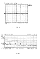
- FIG. 3 shows the measured noise voltage across node 2 and node 8 without deploying winding 46 , voltage-dividing elements 48 and 50 , series element 54 are replaced by a bypass capacitor of 1500pF.
- FIG. 4 shows the corresponding measured common mode current spectrum.
- FIG. 5 shows the measured noise voltage across node 2 and node 8 with the use of winding 46, voltage-dividing elements 48 and 50, series element 54 as illustrated in FIG. 2.
- the turns ratio of windings 36, 38 and 46 are 30:10:3 and the values for series element 54, and voltage dividing elements 50 and 48 are 1500pF, 470pF and 6800pF respectively (which straightforwardly provide the respective impedance values).
- series element 54 has the same value as the bypass capacitor used in the previous case for fair comparison.
- a comparison of FIGS. 3 and 5 reveals a significant reduction in the noise voltage across node 2 and node 8 .
- the corresponding improved, relative to FIG. 4 common mode current spectrum is shown in FIG. 6 .
- FIG. 7 shows a second embodiment of the invention for providing a counter-acting voltage to reduce common mode current with the aid of an amplifying device to amplify a noise signal to provide a counter-acting voltage.
- the amplifying device in this embodiment is a four-terminal amplifying device formed by transistors 76 and 78 with input nodes 86 and output nodes 84 .
- the amplifying device is driven by winding 46 , which provides power to the aforesaid amplifying device via diode 70 and across smoothing capacitor 70 .
- the input nodes 86 sense the noise voltage across series element 54.
- Transistors 76 and 78 connected to provide a totem pole driver to implement a buffer circuit, generate amplify the sensed noise voltage and provide a corresponding counter-acting voltage across output nodes 84.
- the input of the totem pole driver receives the noise voltage across series element 54 and the output terminals of the totem pole driver across output nodes 84 produces the required counter-acting voltage.
- the totem pole output has a phase opposite to that of the noise voltage and cancels out the noise voltage between node 2 and node 8 thus reducing the common mode current.
- FIG. 7 is illustrative and other amplification providing architectures are intended to be within the scope of the invention.
- FIG. 8 shows the measured noise voltage across node 2 and node 8 with the use of the amplifying architecture of FIG. 7.
- a comparison of FIG.S 3 and 8 reveals a significant reduction in the noise voltage across node 2 and node 8 along with the corresponding common mode current spectrum shown in FIG. 9 , which, in turn, reveals the reduction in the common mode current compared to FIG. 4 .
- FIG. 10 is an exemplary implementation utilizing an amplifying device similar to the second embodiment described above.
- This embodiment shows a power converter with at least one switching circuit 96 and at least one rectifying module 9 4.
- the four terminal amplifying device is implemented with a buffer amplifier 90.
- Buffer input 84 and output 86 share a common node as shown.
- Input terminals 84 sense noise voltage across the series element 54 and generate the counter-acting voltage as described before. Since the gain of buffer amplifier 90 generates counter-acting voltage sufficient for cancellation of the noise voltage across series element 54 , no amplitude adjustment is required.
- the amplifier gain in general, is greater than one in many embodiments of the invention. In other words, the specification of the amplifier gain is not a limitation on the possible embodiments.
- Element 92 provides frequency compensation, if required, depending on the frequency response of buffer 90 over the noise frequency range.
- Series element 54 enables coupling of counter-acting voltage.
- FIG. 11 illustrates another embodiment of the invention comprising a power converter with an isolation transformer.
- An amplifier 100 represented by a four terminal device has a pair of input 104 and output 106 terminals.
- Input terminal 104 accepts a signal corresponding to noise voltage between converter primary and secondary side as shown.
- Output terminal 106 produces a corresponding counter-acting voltage. The principle of operation is explained next.
- the third embodiment shown in FIG. 11 makes use of amplifying component to generate the counter-acting voltage to cancel out noise voltage across secondary common node 8 and primary switching circuit input terminal 2 .
- Active component 100 generates the counter-acting voltage.
- this embodiment senses noise voltage across nodes 2 and 8 of the primary and the secondary non-switching nodes directly. Counter-acting voltage is then generated at the output terminals of active component 100 connected across the output 106 comprising secondary node 8 and across an impedance element 102 connected back to the primary input node 2 .
- element 108 can also be connected to other nodes with very low impedance to node 2 , a typical example of such node is node 58 since the capacitance of input capacitor 60 is usually large enough to provide a low impedance path at the noise frequency.
- Element 102 is connected across active component 100 for frequency compensation in practical case. It should be noted that the active component 100 must be able to provide enough gain at frequencies concerned in order to minimize error voltage which may produce common mode current flowing through parasitic capacitance 10 and power source impedance to earth 6 . In addition, some protection circuit may be required to protect the active component in order to withstand high isolation voltage between the primary and secondary as required by many safety standards.
- FIG. 12 is another implementation similar to the third embodiment described above.
- the four terminal amplifying device is implemented by an operational amplifier 110 and a coupling capacitor 120 for retaining isolation between primary and secondary.
- the input terminals of operational amplifier 110 sense the noise voltage across the primary and secondary non-switching nodes 2 and 8 respectively through coupling capacitor 120 .
- the operational amplifier 110 generates a counter-acting voltage at output terminals 116 .
- the counter-acting voltage is connected between the primary and secondary nodes 2 and 8 through capacitor 118 to cancel out noise across these two nodes as described before.
- the embodiments described herein and the principles in accordance with the invention cover devices and systems for reducing EMI.
- they include a common mode noise reducing apparatus for reduction of common mode noise in a switching power converter with an input terminal and an output terminal.
- the common mode noise reducing apparatus includes means for sensing a signal potential difference corresponding to a potential difference between the output terminal of the switching power converter and the input terminal of the switching power converter.
- the term terminal includes one of, for instance, two leads used to electrical power or signals.
- the apparatus further includes a voltage-generating source responsive to the signal potential difference for generating a counter-acting voltage. This counter-acting voltage reduces the potential difference between the output terminal and the input terminal of the switching power converter.
- a series impedance is coupled to the voltage generating source in a path linking the at least one input terminal and the at least one output terminal via at least one capacitor.
- the voltage generating source of the aforementioned common mode noise reducing apparatus can be implemented as a counter-acting winding coupled to a primary winding and to a secondary winding in a power transformer in the switching power converter.
- the voltage generating source of the aforementioned common mode noise reducing apparatus is an amplifying device receiving the signal potential difference as an input signal and producing a counter-acting voltage.
- the means for sensing the signal potential difference include an impedance connected in series in a path linking the input terminal and the output terminal of the switching power converter.
- the means for sensing the signal potential difference include a counter-acting winding coupled to the primary winding and to the secondary winding.
- an electromagnetic noise-filtering element is advantageously employed to selectively reduce current contributing to the generation of objectionable EMI.
- a typical system for converting power with low common mode noise includes a switching power converter having an input terminal and an output terminal with a counter-acting winding coupled to an inductive component, and a capacitor coupled in series to the counter-acting winding to provide isolation between the output and the input.
Landscapes
- Engineering & Computer Science (AREA)
- Theoretical Computer Science (AREA)
- Manufacturing & Machinery (AREA)
- Mechanical Engineering (AREA)
- Physics & Mathematics (AREA)
- General Engineering & Computer Science (AREA)
- General Physics & Mathematics (AREA)
- Power Engineering (AREA)
- Dc-Dc Converters (AREA)
- Amplifiers (AREA)
Applications Claiming Priority (2)
| Application Number | Priority Date | Filing Date | Title |
|---|---|---|---|
| US939068 | 1997-09-29 | ||
| US09/939,068 US6490181B1 (en) | 2001-08-24 | 2001-08-24 | Apparatus for reducing common mode noise current in power converters |
Publications (3)
| Publication Number | Publication Date |
|---|---|
| EP1289108A2 true EP1289108A2 (fr) | 2003-03-05 |
| EP1289108A3 EP1289108A3 (fr) | 2005-06-15 |
| EP1289108B1 EP1289108B1 (fr) | 2011-07-20 |
Family
ID=25472487
Family Applications (1)
| Application Number | Title | Priority Date | Filing Date |
|---|---|---|---|
| EP02018555A Expired - Lifetime EP1289108B1 (fr) | 2001-08-24 | 2002-08-17 | Appareil pour réduire le bruit de courant dans les convertisseurs de puissance |
Country Status (3)
| Country | Link |
|---|---|
| US (2) | US6490181B1 (fr) |
| EP (1) | EP1289108B1 (fr) |
| CN (1) | CN1201469C (fr) |
Families Citing this family (31)
| Publication number | Priority date | Publication date | Assignee | Title |
|---|---|---|---|---|
| US6104622A (en) * | 1997-04-30 | 2000-08-15 | Fidelix Y.K. | Power supply apparatus for reduction of power consumption |
| US6490181B1 (en) * | 2001-08-24 | 2002-12-03 | The University Of Hong Kong | Apparatus for reducing common mode noise current in power converters |
| US6879500B2 (en) * | 2001-08-24 | 2005-04-12 | The University Of Hong Kong | Apparatus for noise current reduction in power converters |
| WO2003058791A2 (fr) * | 2002-01-07 | 2003-07-17 | International Rectifier Corporation | Filtre anti-perturbation electromagnetique a annulation aval |
| NZ518966A (en) * | 2002-05-15 | 2004-12-24 | Enatel Ltd | Passive common mode noise reduction circuit by applying anti-phase noise (using a further winding, capacitor) |
| US6850423B2 (en) * | 2003-05-30 | 2005-02-01 | Comarco Wireless Technologies, Inc. | Common mode noise cancellation circuit |
| US9153960B2 (en) | 2004-01-15 | 2015-10-06 | Comarco Wireless Technologies, Inc. | Power supply equipment utilizing interchangeable tips to provide power and a data signal to electronic devices |
| US6958594B2 (en) * | 2004-01-21 | 2005-10-25 | Analog Devices, Inc. | Switched noise filter circuit for a DC-DC converter |
| DE602006019471D1 (de) * | 2005-10-10 | 2011-02-17 | Texas Instr Cork Ltd | Stromwandler |
| US7545656B2 (en) * | 2006-07-18 | 2009-06-09 | Comarco Wireless Technologies, Inc. | Common mode noise reduction circuit utilizing dual primary windings |
| US20090195303A1 (en) * | 2008-02-04 | 2009-08-06 | William Joseph Bowhers | Method of Reducing Common Mode Current Noise in Power Conversion Applications |
| US8138620B2 (en) * | 2009-06-12 | 2012-03-20 | General Electric Company | Methods and systems for operating a wind turbine power converter |
| US8772975B2 (en) * | 2009-12-07 | 2014-07-08 | Qualcomm Incorporated | Apparatus and method for implementing a differential drive amplifier and a coil arrangement |
| JP5721355B2 (ja) * | 2010-07-21 | 2015-05-20 | キヤノン株式会社 | 電源回路 |
| US8692526B2 (en) | 2010-12-01 | 2014-04-08 | Microsoft Corporation | Converting leakage current to DC output |
| US9276460B2 (en) * | 2012-05-25 | 2016-03-01 | Flextronics Ap, Llc | Power converter with noise immunity |
| EP2709250A1 (fr) * | 2012-09-13 | 2014-03-19 | Nxp B.V. | Filtrage de bruit |
| CN102868380A (zh) * | 2012-09-20 | 2013-01-09 | 无锡莱吉特信息科技有限公司 | 一种共模滤波电路 |
| US9490651B2 (en) | 2013-03-15 | 2016-11-08 | Flextronics Ap, Llc | Sweep frequency mode for magnetic resonant power transmission |
| US9564823B2 (en) | 2014-10-01 | 2017-02-07 | Toyota Motor Engineering & Manufacturing North America, Inc. | DC-DC power conversion circuit with magnetic and capacitive isolation |
| US9866132B2 (en) * | 2015-07-31 | 2018-01-09 | Toyota Motor Engineering & Manufacturing North America, Inc. | DC-DC power conversion and balancing circuit |
| US9893631B2 (en) | 2015-09-23 | 2018-02-13 | Toyota Motor Engineering & Manufacturing North America, Inc. | Non-isolated DC-DC conversion circuit configured for capacitive and magnetic power transfer |
| US10038369B2 (en) * | 2015-11-19 | 2018-07-31 | Pacesetter, Inc. | Systems and methods for reducing noise and interference in isolated switching power supplies |
| EP3232551B1 (fr) | 2016-04-15 | 2020-08-19 | Nxp B.V. | Alimentation électrique à mode commuté avec filtre anti-bruit |
| US10333410B2 (en) * | 2016-09-15 | 2019-06-25 | Futurewei Technologies, Inc. | Common-mode (CM) electromagnetic interference (EMI) reduction in resonant converters |
| CN107248815B (zh) * | 2017-06-07 | 2020-04-28 | 浙江大学 | 低emi非对称中心抽头整流电路 |
| WO2020142568A1 (fr) * | 2018-12-31 | 2020-07-09 | Rompower Technology Holdings, Llc | "blindage actif rompower" transformateur de puissance pour injection minimale de bruit entre un enroulement primaire et un enroulement secondaire |
| US11325714B2 (en) | 2020-07-09 | 2022-05-10 | General Electric Company | Electric power system for a vehicle |
| US12322535B2 (en) | 2020-11-11 | 2025-06-03 | Rompower Technology Holdings, Llc | Planar multilayer transformer with minimum noise injection in between primary and secondary winding |
| US11750114B2 (en) | 2021-10-22 | 2023-09-05 | General Electric Company | Reduction of common mode emission of an electrical power converter |
| US12438439B2 (en) * | 2023-01-31 | 2025-10-07 | Apple Inc. | Common mode noise cancellation for LLC resonant converters |
Family Cites Families (13)
| Publication number | Priority date | Publication date | Assignee | Title |
|---|---|---|---|---|
| US4683529A (en) * | 1986-11-12 | 1987-07-28 | Zytec Corporation | Switching power supply with automatic power factor correction |
| US4888675A (en) * | 1987-08-26 | 1989-12-19 | Harris Corporation | Switching power supply filter |
| JPH03230764A (ja) * | 1990-02-01 | 1991-10-14 | Toshiba Corp | Pwm制御による電源装置 |
| US5077543A (en) * | 1991-02-07 | 1991-12-31 | Ungermann-Bass, Inc. | Balanced low-pass common mode filter |
| JP3392915B2 (ja) * | 1993-07-19 | 2003-03-31 | 株式会社リコー | 電子機器用電源装置 |
| US5319535A (en) * | 1993-08-19 | 1994-06-07 | Westinghouse Electric Corp. | Active power line conditioner having capability for rejection of common-mode disturbances |
| US5636112A (en) * | 1995-07-13 | 1997-06-03 | Compaq Computer Corporation | Portable computer having built-in AC adapter incorporating a space efficient electromagnetic interference filter |
| US6122184A (en) * | 1997-06-19 | 2000-09-19 | The Texas A&M University System | Method and system for an improved converter output filter for an induction drive system |
| US5905642A (en) * | 1997-11-11 | 1999-05-18 | Robicon Corporation | Apparatus and method to reduce common mode voltage from current source drives |
| US6288915B1 (en) * | 1997-12-23 | 2001-09-11 | Asea Brown Boveri Ag | Converter circuit arrangement having a DC intermediate circuit |
| KR100494256B1 (ko) * | 1998-04-28 | 2005-06-13 | 마츠시타 덴끼 산교 가부시키가이샤 | 다리미 |
| US6137392A (en) * | 1998-10-05 | 2000-10-24 | Herbert; Edward | Transformer for switched mode power supplies and similar applications |
| US6490181B1 (en) * | 2001-08-24 | 2002-12-03 | The University Of Hong Kong | Apparatus for reducing common mode noise current in power converters |
-
2001
- 2001-08-24 US US09/939,068 patent/US6490181B1/en not_active Expired - Lifetime
-
2002
- 2002-08-17 EP EP02018555A patent/EP1289108B1/fr not_active Expired - Lifetime
- 2002-08-24 CN CNB021420572A patent/CN1201469C/zh not_active Expired - Lifetime
- 2002-12-02 US US10/308,994 patent/US20030231515A1/en not_active Abandoned
Also Published As
| Publication number | Publication date |
|---|---|
| US6490181B1 (en) | 2002-12-03 |
| CN1407702A (zh) | 2003-04-02 |
| EP1289108A3 (fr) | 2005-06-15 |
| EP1289108B1 (fr) | 2011-07-20 |
| US20030231515A1 (en) | 2003-12-18 |
| CN1201469C (zh) | 2005-05-11 |
| HK1054628A1 (en) | 2003-12-05 |
Similar Documents
| Publication | Publication Date | Title |
|---|---|---|
| US6490181B1 (en) | Apparatus for reducing common mode noise current in power converters | |
| US6879500B2 (en) | Apparatus for noise current reduction in power converters | |
| EP2787618B1 (fr) | Filtre anti-perturbation électromagnétique actif en aval d'alimentation en tension | |
| US5956246A (en) | Low-noise switching power supply | |
| US7369026B2 (en) | Method and apparatus for substantially reducing electrical displacement current flow between input and output circuits coupled to input and output windings of an energy transfer element | |
| US7898827B2 (en) | Active EMI filtering using magnetic coupling cancellation | |
| WO2002037674A1 (fr) | Filtre antiparasite pour ligne a haute tension | |
| EP0602834A1 (fr) | Circuits de commande de tension | |
| US8379415B2 (en) | Systems and methods for reducing EMI in switch mode converter systems | |
| US7672147B1 (en) | High attenuation filtering circuit for power converters | |
| US7193869B2 (en) | Noise suppressor | |
| EP4080751A1 (fr) | Convertisseur cc/cc et alimentation électrique de communication | |
| US6347045B1 (en) | Noise canceling apparatus for a power converter | |
| EP4005077B1 (fr) | Circuit de suppression d'interférence électromagnétique et circuit de détection associé | |
| Zhu et al. | Design and evaluation of an active ripple filter with Rogowski-coil current sensing | |
| US10886857B1 (en) | Inhibiting noise coupling across isolated power supplies | |
| US7554825B2 (en) | Switching power supply capable of reducing low-frequency secondary-side common-mode voltage | |
| US6920053B2 (en) | Active EMI filter having no inductive current sensing device | |
| JP2005117218A (ja) | ノイズ抑制回路 | |
| US20260039278A1 (en) | Active compensation device providing electromagnetic wave noise data | |
| HK1054628B (en) | Apparatus for noise current reduction in power converters | |
| WO2024049788A1 (fr) | Filtre emi en mode commun | |
| JPWO2020255247A1 (ja) | 漏れ電流低減装置 |
Legal Events
| Date | Code | Title | Description |
|---|---|---|---|
| PUAI | Public reference made under article 153(3) epc to a published international application that has entered the european phase |
Free format text: ORIGINAL CODE: 0009012 |
|
| AK | Designated contracting states |
Kind code of ref document: A2 Designated state(s): AT BE BG CH CY CZ DE DK EE ES FI FR GB GR IE IT LI LU MC NL PT SE SK TR Designated state(s): AT BE BG CH CY CZ DE DK EE ES FI FR GB GR IE IT LI LU MC NL PT SE SK TR |
|
| AX | Request for extension of the european patent |
Extension state: AL LT LV MK RO SI |
|
| PUAL | Search report despatched |
Free format text: ORIGINAL CODE: 0009013 |
|
| AK | Designated contracting states |
Kind code of ref document: A3 Designated state(s): AT BE BG CH CY CZ DE DK EE ES FI FR GB GR IE IT LI LU MC NL PT SE SK TR |
|
| AX | Request for extension of the european patent |
Extension state: AL LT LV MK RO SI |
|
| 17P | Request for examination filed |
Effective date: 20051020 |
|
| AKX | Designation fees paid |
Designated state(s): DE FR GB |
|
| 17Q | First examination report despatched |
Effective date: 20071011 |
|
| GRAP | Despatch of communication of intention to grant a patent |
Free format text: ORIGINAL CODE: EPIDOSNIGR1 |
|
| GRAS | Grant fee paid |
Free format text: ORIGINAL CODE: EPIDOSNIGR3 |
|
| GRAA | (expected) grant |
Free format text: ORIGINAL CODE: 0009210 |
|
| AK | Designated contracting states |
Kind code of ref document: B1 Designated state(s): DE FR GB |
|
| REG | Reference to a national code |
Ref country code: GB Ref legal event code: FG4D |
|
| REG | Reference to a national code |
Ref country code: DE Ref legal event code: R096 Ref document number: 60240533 Country of ref document: DE Effective date: 20110908 |
|
| PLBE | No opposition filed within time limit |
Free format text: ORIGINAL CODE: 0009261 |
|
| STAA | Information on the status of an ep patent application or granted ep patent |
Free format text: STATUS: NO OPPOSITION FILED WITHIN TIME LIMIT |
|
| 26N | No opposition filed |
Effective date: 20120423 |
|
| GBPC | Gb: european patent ceased through non-payment of renewal fee |
Effective date: 20111020 |
|
| REG | Reference to a national code |
Ref country code: FR Ref legal event code: ST Effective date: 20120525 |
|
| REG | Reference to a national code |
Ref country code: DE Ref legal event code: R097 Ref document number: 60240533 Country of ref document: DE Effective date: 20120423 |
|
| PG25 | Lapsed in a contracting state [announced via postgrant information from national office to epo] |
Ref country code: GB Free format text: LAPSE BECAUSE OF NON-PAYMENT OF DUE FEES Effective date: 20111020 Ref country code: FR Free format text: LAPSE BECAUSE OF NON-PAYMENT OF DUE FEES Effective date: 20110920 |
|
| PGFP | Annual fee paid to national office [announced via postgrant information from national office to epo] |
Ref country code: DE Payment date: 20210706 Year of fee payment: 20 |
|
| REG | Reference to a national code |
Ref country code: DE Ref legal event code: R071 Ref document number: 60240533 Country of ref document: DE |