EP1291879A2 - Resistiver Speicherarray - Google Patents
Resistiver Speicherarray Download PDFInfo
- Publication number
- EP1291879A2 EP1291879A2 EP02255690A EP02255690A EP1291879A2 EP 1291879 A2 EP1291879 A2 EP 1291879A2 EP 02255690 A EP02255690 A EP 02255690A EP 02255690 A EP02255690 A EP 02255690A EP 1291879 A2 EP1291879 A2 EP 1291879A2
- Authority
- EP
- European Patent Office
- Prior art keywords
- row
- resistance
- column
- values
- array
- Prior art date
- Legal status (The legal status is an assumption and is not a legal conclusion. Google has not performed a legal analysis and makes no representation as to the accuracy of the status listed.)
- Withdrawn
Links
Images


Classifications
-
- G—PHYSICS
- G11—INFORMATION STORAGE
- G11C—STATIC STORES
- G11C11/00—Digital stores characterised by the use of particular electric or magnetic storage elements; Storage elements therefor
- G11C11/02—Digital stores characterised by the use of particular electric or magnetic storage elements; Storage elements therefor using magnetic elements
- G11C11/14—Digital stores characterised by the use of particular electric or magnetic storage elements; Storage elements therefor using magnetic elements using thin-film elements
- G11C11/15—Digital stores characterised by the use of particular electric or magnetic storage elements; Storage elements therefor using magnetic elements using thin-film elements using multiple magnetic layers
-
- G—PHYSICS
- G11—INFORMATION STORAGE
- G11C—STATIC STORES
- G11C11/00—Digital stores characterised by the use of particular electric or magnetic storage elements; Storage elements therefor
- G11C11/02—Digital stores characterised by the use of particular electric or magnetic storage elements; Storage elements therefor using magnetic elements
- G11C11/16—Digital stores characterised by the use of particular electric or magnetic storage elements; Storage elements therefor using magnetic elements using elements in which the storage effect is based on magnetic spin effect
- G11C11/165—Auxiliary circuits
- G11C11/1673—Reading or sensing circuits or methods
Definitions
- the present invention pertains to the field of resistive memory cell arrays. More particularly, this invention relates to methods and structure for memory in a resistive memory array for maximizing the signal to noise ratio of the array.
- a resistive random access memory is a cross point type memory array of a planar matrix of spaced memory cells sandwiched between two meshes of conductors running in orthogonal directions above and below the cells.
- An example is the resistive RAM array 10 shown in Figure 1.
- the row conductors 12 running in one direction are referred to as the word lines, and the column conductors 14 extending in a second direction usually perpendicular to the first direction are referred to as the bit lines.
- the memory cells 16 are usually arranged in a square or rectangular array so that each memory cell unit 16 is connected with one word line 12 and an intersecting bit line 14.
- the resistance of each memory cell has more than one state, and the data in the memory cell is a function of the resistive state of the cell.
- the resistive memory cells may include one or more magnetic layers, a fuse or anti-fuse, or any element that stores or generates information by affecting the magnitude of the nominal resistance of the element.
- Other types of resistive elements used in a resistive RAM array include poly-silicon resistors as part of a read-only memory, and floating gate transistors as part of optical memory, imaging devices or floating gate memory devices.
- MRAM magnetic random access memory
- each memory cell is formed of a plurality of magnetic layers separated by insulating layers.
- One magnetic layer is called a pinned layer, in which the magnetic orientation is fixed so as not to rotate in the presence of an applied magnetic field in the range of interest.
- Another magnetic layer is referred to as a sense layer, in which the magnetic orientation is variable between a state aligned with the state of the pinned layer and a state in misalignment with the state of the pinned layer.
- An insulating tunnel barrier layer sandwiches between the magnetic pinned layer and the magnetic sense layer. This insulating tunnel barrier layer allows quantum mechanical tunneling to occur between the sense layer and the pinned layer.
- the tunneling is electron spin dependent, causing the resistance of the memory cell, a function of the relative orientations of the magnetizations of the sense layer and the pinned layer.
- the variations in the junction resistance for the two states of the sense layer determine the data stored in the memory cell.
- U.S. Patent 6,169,686, granted to Brug et al. on January 2, 2001 discloses such a magnetic memory cell memory.
- Memory unit 16 is shown as a three-layer memory cell 20.
- Memory unit 16 is shown as a three-layer memory cell 20.
- a bit of information is stored according to the orientation of a magnetic sense layer 22 of the cell 20.
- the cell 20 has two stable magnetic states corresponding to the logic states "1" and "0.”
- the two-way arrow 15 on the sense layer 22 shows this binary-state capability.
- a pinned layer 24 in the cell 20 is separated from the sense layer by a thin insulator 26.
- Pinned layer 24 has a fixed magnetic orientation, such as shown by the one-way arrow 17 on layer 24.
- the cell magnetization When the magnetic state of the sense layer 22 is oriented in the same direction as the direction of the magnetization of the pinned layer 24, the cell magnetization is referred to as "parallel.” Similarly, when the magnetic state of the sense layer 22 is oriented in the direction opposite to the direction of the magnetization of the pinned layer 24, the cell magnetization is referred to as "anti-parallel.” These orientations correspond to a low resistance state and a high resistance state, respectively.
- the magnetic state of a selected memory cell 20 may be changed by applying currents to a word line 12 and a bit line 14 crossing the selected memory cell.
- the currents produce two orthogonal magnetic fields that, when combined, will switch the magnetic orientation of the selected memory cell 20 between the parallel and anti-parallel states.
- Other unselected memory cells receive only a magnetic field from either the word line or the bit line crossing the unselected memory cells. The single field is not strong enough to change the magnetic orientation of the unselected cells, so they retain their magnetic orientation.
- a sense amplifier 32 is connected to the bit line 34 of a selected memory cell 36.
- a voltage V r is applied to the word line 38 of the selected memory cell 36, and sense amplifier 32 applies a voltage to the bit line 34 of cell 36.
- the sense amplifier 32 provides an amplified output 39 reflecting the state of the memory cell 36.
- the same bit line voltage is applied to all of the bit line 34, effectively biasing all the cells on unselected rows to zero potential. This action isolates the bit line currents from one another, effectively blocking most of the leakage current that might otherwise flow through secondary paths, possibly causing errors in the sensing function of the selected memory cell.
- the conductors of the word lines and bit lines in the magnetic array all have some amount of resistance to the flow of electricity through the lines. Also, a low resistance state and a high resistance state, corresponding to memory states "0" and "1" across the junction of the cross point cell. Although the effects of each such resistance is negligible in itself, the combined effect of these resistances in an array, particularly the conductor resistances, causes some reduction in the available sense current for the sense amplifier to determine the states "0" and "1" of the memory cell. If the array becomes too large, the conductor resistances increase because there are more rows and columns. Thus, more current is flowing, and the leakage current through the "sneak paths" also increases.
- the "magneto-resistive tunnel junction” (MTJ) junction of each memory cell in a MRAM array can also be a factor.
- MTJ magnetic-resistive tunnel junction
- a "tunneling current" across the junction of each memory cell is a function of the MTJ resistance of each memory cell and can also contribute to the noise of the array.
- the MTJ resistance across the junction is affected by the material used in the cell and the respective polarizations of the layers on each side of the junction. See Sharma, et al "Spin-dependent tunneling junctions with AIN and AION barriers," 77 Applied Physics Letters, number 14, October 2, 2000.
- an optimal resistance range of the memory cell and an optimal size of a memory array for a given conductor resistance in order to minimize undesirable error contribution to the output signal.
- Ability to detect data in the array is measured in terms of signal-to-noise ratio (SNR); higher SNR results in a lower error rate.
- SNR is usually measured in decibels (dB).
- the present invention provides a method of designing a random access (RAM) memory array having resistive elements for optimizing the signal-to-noise ratio for the array.
- a plurality of memory cells are selected and spaced from each other in a matrix of rows and columns, each memory cell being selected to have a junction resistance values between 0.25 megaohms and 3.60 megaohms.
- a plurality of conductive row lines are connected between the memory cells in a row and are selected to have a row unit line unit resistance of values between substantially 0.0 ohms and 0.38 ohms.
- a plurality of conductive column lines are connected between the memory cells in a column and are selected to have a column unit line unit resistance between memory cells, the row unit line unit resistance being approximately equal to the column unit line unit resistance.
- the values of the memory cell junction resistance are correlated with the values of the row and column unit line resistance so that the signal to noise ratio of the memory array is maintained at 20 decibels or greater.
- a resistive random access memory array has selected elements with resistances correlated to maintain a signal-to-noise ratio of 20 decibels or more for the array.
- a plurality of memory cells are spaced from each other in a matrix of rows and columns, each memory cell being selected to have a junction resistance between 0.80 megaohms and 2.80 megaohms.
- a plurality of conductive row lines connect between the memory cells in a row are selected to have a determined row unit line resistance between memory cells having values in the range of substantially 0.0 ohms to 0.38 ohms.
- a plurality of conductive column lines are connected between the memory cells in a column and are selected to have a column unit line resistance having values in the range of substantially 0.0 ohms to 0.38 ohms.
- the memory cells are selected so that the junction resistance values are correlated with the row or column unit line resistance values, to maintain the signal to noise ratio at 20 decibels or more in the resistive memory array.
- an optimal design for a 1,024 by 1,024 memory cell array in which the row or column unit line resistance values are selected to be between approximately 0.24 ohms and 0.38 ohms, the range of junction resistance values is selected to be between 0.8 megaohms and 2.8 megaohms. Stated in broad terms, the junction resistance values and column and row unit line resistance values are selected so that the ratio of junction resistance values to row or column unit line resistance values is approximately five million to one.
- a magnetic random access memory (MRAM) array has resistive elements with resistances established to maximize a signal-to-noise ratio of at least 20 decibels for the array.
- a plurality of magnetic-resistive tunnel junction (MTJ) memory cells are selected and spaced from each other in a square matrix of approximately N rows and N columns, each memory cell being selected to have an MTJ resistance of between 0.25 megaohms and 3.60 megaohms.
- a plurality of conductive row lines are connected between the memory cells in each row, each row line being selected to have a total row line resistance of N times the row unit resistance between memory cells.
- a plurality of conductive column lines are connected between the memory cells in each column, each column line being selected to have a total column line resistance of N times the column unit resistance between memory cells.
- the row and column conductors are selected so that the total row line resistance for each row is approximately equal to the total column line resistance for each column.
- the MTJ resistance values and row and column conductor resistance values are selected so that the ratio of the MTJ resistance values to the total row or column line resistance values must be greater than approximately five million to N to maintain a signal-to-noise ratio of 20 decibels or more for the memory array.
- N is equal to approximately 1024
- the MTJ resistance values are correlated with the row and column total line resistance values so that the ratio of MTJ resistance to total row or column line resistance is approximately 5,000 or greater.
- one preferred embodiment of the present invention is an MRAM memory cell array 40.
- the MRAM device 40 includes an array of memory cells 42 arranged in rows 44 and columns 46, with the rows 44 extending along an x-direction and the columns 46 extending along a y-direction. Only a relatively small number of memory cells 42 are shown to simplify the description of the invention. In practice arrays of 1024 by 1024 memory cells or larger are used and the number of memory cells in the rows may not be the same as the number of memory cells in the columns.
- Conductors 48 functioning as word lines extend along the x-direction in a plane on one side of the memory cell array 40.
- Conductors 49 functioning as bit lines extend along the y-direction in a plane on the other side of the memory cell array 40.
- Each memory cell 42 is located at a crossing point of a corresponding word line 48 and bit line 49.
- the memory cells 42 are not limited to any particular type of device.
- a spin dependent tunneling device may be used, as described above.
- Data is stored in the memory cells 42 by orienting the magnetization of each cell to represent a "1" or a "0.”
- the logic value of "0" may be stored in the memory cell 42 by orienting the magnetization of the sense layer to be parallel to the magnetic orientation of the pinned layer
- the logic value of "1” may be stored in the memory cell by orienting the magnetization of the sense layer to be opposite in direction, or anti-parallel, to the magnetic orientation of the pinned layer.
- the logic value is stored in a selected memory cell as described above. With a voltage applied to the word line and bit line of the selected cell, the current across the junction of the memory cell determines whether the cell magnetization is parallel or anti-parallel. Preferably, an anti-parallel orientation will cause greater MTJ resistance and thus lower current across the junction of the selected memory cell. Preferably, each memory cell retains the magnetic orientation in the absence of power, thus being referred to as "non-volatile.”
- Graph 50 in Figure 4B shows the variations in applied voltage along a word line 52.
- Arrows 54, 56 and 58 along word line 52 illustrate the current flow and voltage drop as current progresses along word line 52.
- an initially applied voltage of 0.50 volts at the beginning of the word line 52 will drop to less than 0.45 volts at the end of a conductor connecting 1,000 memory cells.
- the graph 60 in Figure 4C shows the resultant leakage current due to column conductor resistance with respect to the row location.
- the leakage current is about 1.1 x 10 -8 amperes and reduces to effectively zero at the last row conductor connecting 1,000 memory cells.
- the row further away from the sense amplifier suffers more leakage current than the rows near the sense amplifier because conductor resistance is larger.
- a contour plot 70 is given, showing the signal-to-noise ratio in decibels as a function of conductor unit resistance in ohms (y-axis) and MTJ resistance of a memory cell in megaohms (x-axis).
- a conductor unit resistance above the dashed line 78 can be easily manufactured with existing fabrication processes and commonly used metals, such as copper, aluminum or aluminum copper alloy.
- a lower conductor resistance unit is possible by increasing the width and thickness of the conductor, but this will have a detrimental effect by causing the size of the array to increase, so that more current is needed to write data to the array.
- a new development metal alloy or super conductor is preferred to lower the unit conductor resistance, but they may be impractical at the present time.
- a 20 decibels contour line 72 has been determined to represent a threshold below which the SNR should not drop in order to maintain acceptable low levels of error rates in the array. Below the contour line 72, the SNR will be higher than 20. It is preferred that the SNR be above line 78 (0.24 ohms) for ease in manufacturing, but below line 72 to maintain an acceptable SNR. Thus, the optimal design range is shown by the shaded area 74 in Figure 5 bounded by the 20 dB contour line 72 and the dashed line 78. In this range the unit conductor resistance and the MTJ resistance range are optimal for the memory array while still maintaining a 20 dB SNR or better.
- row and column conductors should be selected having a conductor unit resistance below about 0.38 ohms in order to keep the SNR at or above 20 decibels.
- the row and column conductors are selected having a unit resistance in the range of substantially 0.0 ohms to 0.38 ohms, if the conductor range is available.
- the row and column unit resistances are assumed to be the same.
- the scope of the present invention is intended to include different row and column unit resistances, as long as they each fall within the range between substantially 0.0 ohms and 0.38 ohms.
- the number of rows and columns may differ, depending on the circuitry design.
- the memory cells are selected so that the MTJ resistance of each memory cell is between about 0.25 megaohms and 3.60 megaohms, preferably in the range of about 0.8 megaohms to 2.8 megaohms, depending on the unit conductor resistance.
- the memory cell junction values are then correlated with the row and column unit line resistance values to provide a signal-to-noise ratio of at least 20 decibels in the memory array.
- this area is designated as area 75 for an SNR between 20 and 25 dB, and area 76 for an SNR above 25 dB. These areas represent ranges of resistive elements that are harder to achieve, particularly for area 76. However, they may be achievable with special conditions, as mentioned earlier, and are included within the scope of the present invention.
- Conductor unit resistance will vary depending on the size of the array, since thinner conductors are needed as the array becomes larger. Thus, to some degree, the size of the array will determine the conductor unit resistance. For an array of about 1,024 by 1,024 memory cells, a conductor unit resistance of about 0.24 ohms could preferably be selected, indicated by dotted line 78. The intersections of dotted line 78 with contour line 72 at points 71 and 73 define the acceptable range of MTJ resistance values to be between about 0.8 megaohms and 2.8 megaohms.
- the total resistance of each row is 246 ohms and the total resistance of each column is 246 ohms.
- the memory cells are selected so that the range of MTJ resistance values is between 0.8 megaohms and 2.8 megaohms. This information is extremely valuable for circuit designers in maintaining acceptable SNR levels for a typical memory array.
- Figure 5 shows a maximum value, at point 77, of about 0.38 ohms, above which the conductor unit line resistance values should not go.
- contour line 72 in Figure 5 indicates that for the highest conductor unit line resistance value of about 0.38, the memory cells should be selected to have an MTJ resistance value of about 1.8 megaohms.
- the MTJ resistance values and row and column unit line resistance values are selected so that the approximate ratio of MTJ resistant to conductor unit line resistance is about 1.8 x 10 +6 to 3.8 x 10 -1 or, roughly about five million to one.
- the memory cells and row and column conductors are chosen so that the MTJ resistance values are correlated with the row and column unit line resistance values to provide a signal-to-noise ratio of at least 20 decibels in the memory array.
- the effective ratio of MTJ resistance to total line resistance for a given number of memory elements N in a row and a given number of memory elements M in a column.
- the total line resistance of a conductor for the maximum acceptable conductor unit line resistance value is 0.38 ohms times the number of memory elements N in a conductor line.
- the optimal MTJ memory cell resistance value is about 1.8 megaohms. Therefore, the ratio of MTJ memory cell resistance to total conductor line resistance is about 1.8 x 10 +6 to 3.8 x 10 -1 x N, that is about 5 x 10 +6 to one N, or five million to N.
- the ratio of MTJ memory cell resistance to total line resistance is about 5,000 to one.
- the row and column conductors are made of highly conductive materials, such as copper or aluminum or even super conductor materials.
- the pinned layer is composed of anti-ferrous material and the sense layer is composed of magnetic material influenced by a magnetic field, such as nickel iron, cobalt iron or nickel iron cobalt.
- the insulation layer may be composed of any type of insulation material and is very thin, usually not more than ten to fifty angstroms to allow a tunneling current to occur.
- the cell junction resistance states may change between 1.0 megaohms at the low state and 1.3 megaohms for the high state. If a voltage of 0.5 volts is applied across the junction, the resulting current is about 500 nano-amps for the low state and 384 nano-amps for the high state. Thus, for sensing data in the memory cell, the current signal variation or window is typically only about 116 nano-amps in the ideal case. With the loss of signal due to column and row resistance the effective window is even less. Accordingly, careful design of the array elements is essential to maintain a satisfactory signal-to-noise ratio in the array.
- Figures 6, 7 and 8 provide circuitry to accompany the following analysis of the resistances in a resistive array.
- an analysis is giving of the resistance along each row of a memory array.
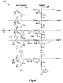
- a resistive array 80 is shown in simplified circuitry having number of rows 1 through m, each having a conductor 82 and having a number of columns 1 through n, each having a conductor 84.
- At the intersection of each row and column conductor is a memory cell 86 connected between the row and column conductors.
- Each row conductor has some resistance to current flowing through it.
- the unit resistance along each row conductor 82 between each memory cell 86 is shown as resistances (r c ) 87, 88 and 89.
- unit resistance 87 causes a voltage drop between column 0 and column 1 so that a slightly lower voltage V 1 is impressed across memory cell 86b resulting in a current I 1 through the memory cell.
- An identical unit resistance 88 is encountered along row 0 between columns 1 and 2, resulting in a voltage V 2 across memory cell 86c causing a current I 2 .
- conductor 82a has a unit resistance between each column conductor 84 down to the last unit resistance 89, resulting in a voltage V n across memory cell 86n and a current I n therethrough. Essentially, the same phenomenon occurs with respect to each row 0 through m along columns 0 through n.
- V 0 V
- V 1 V 0 ⁇ r c (I 1 +I 2 +...I n )
- V 2 V 1 ⁇ r c (I 2 +I 3 +...I n )
- V 3 V 2 ⁇ r c (I 3 +I 4 +...I n )
- V n V n-1 ⁇ r c (I n )
- V 0 V 1
- V 1 V ⁇ r c I (n)
- V 2 V ⁇ r c I [n + (n-1)]
- V 3 V ⁇ r c I [n + (n-1) + (n-2)]
- V n V ⁇ r c I [n + (n-1) + (n-2) + (n-3) ... + 1]
- a resistive array 90 is shown in simplified circuitry having a number of rows 1 through m, each having a conductor 92 and having a number of columns 1 through n, each having a conductor 94.
- a memory cell 96 At the intersection of each row and column conductor is a memory cell 96 connected between the row and column conductors.
- Each row conductor has some resistance to current flowing through it.
- the unit resistance along each row conductor 92 between each memory cell 96 is shown as resistances (r c ) 97, 98 and 99.
- the simplified array 100 in Figure 8 has only two columns, the n column with a column conductor 104, which is the final column and the n-1 column with a combined conductor 102, which is a combination of all of the columns other than the n column.
- a voltage V is applied to the selected row, for example row 2, column n.
- V H (a) V/R L (m-a) r c
- V L (a) V/R H (m-a) r c
- ⁇ V (a) The small difference in voltage, ⁇ V (a), will cause a small leak current ⁇ i (a) to flow through memory cell 110, as shown in Figure 8.
- ⁇ i (a) ⁇ V ( a )
- R L + RL n ⁇ 1 [V/R L ⁇ V/R H ]
- r c (m-a-1) [ 1 R L + R L n ⁇ 1 ]
- I leak (a) [V/R L ⁇ V/R H ] [ 1 R L + R L n ⁇ 1 ] r c . [(m-a) + (m-a-1) + (m-a-2)...]
- the sense current to determine the state of the memory cell will have the largest error due to a large leakage current, I leak .
- m n, and the percent errors due to the row conductors resistance and the column conductor resistance are about the same.
- the conductor thickness is also chosen to optimize the writing of data.
- a narrow and thin conductor is better for writing, but causes relatively high conductor resistance that will reduce the signal-to-noise ratio (SNR). Therefore, the error rate will be relatively high.
- SNR signal-to-noise ratio
- FIG. 9 flow diagrams are provided to further illustrate two preferred methods of the present invention.
- a plurality of memory cells are spaced from each other in a matrix of rows and columns.
- each memory cell is selected to have a junction resistance value between 0,25 megaohms and 3.60 megaohms.
- a plurality of conductive row lines are connected between the memory cells in a plurality of rows.
- each conductive row line is selected to have a unit row resistance between adjacent memory cells, where the unit row resistance of each row has a value between substantially 0.0 ohms and 0.38 ohms.
- each conductive column line is selected to have a unit column resistance between substantially 0.0 ohms and 0.38 ohms.
- the values of the memory cell junction resistance and the values of the row and column unit line resistances are correlated in order to have a signal-to-noise ratio of 20 decibels or greater in the resistive memory array.
- FIG. 10 Another preferred method of the present invention is shown in Figure 10.
- a plurality of memory cells are spaced from each other in a matrix of rows and columns.
- each memory cell is selected to have a junction resistance value between 0,80 megaohms and 2.80 megaohms.
- a plurality of conductive row lines are connected between the memory cells in a plurality of rows.
- each conductive row line is selected to have a unit row resistance between adjacent memory cells, where the unit row resistance of each row has a value between substantially 0.24 ohms and 0.38 ohms.
- a plurality of conductive column lines are connected between the memory cells in a plurality of columns.
- each conductive column line is selected to have a unit column resistance between substantially 0.24 ohms and 0.38 ohms.
- the values of the memory cell junction resistance and the values of the row and column unit line resistances are correlated in order to have a signal-to-noise ratio of 20 decibels or greater in the resistive memory array.
Landscapes
- Engineering & Computer Science (AREA)
- Computer Hardware Design (AREA)
- Semiconductor Memories (AREA)
- Mram Or Spin Memory Techniques (AREA)
- Non-Volatile Memory (AREA)
Applications Claiming Priority (2)
| Application Number | Priority Date | Filing Date | Title |
|---|---|---|---|
| US944680 | 2001-08-31 | ||
| US09/944,680 US6385079B1 (en) | 2001-08-31 | 2001-08-31 | Methods and structure for maximizing signal to noise ratio in resistive array |
Publications (2)
| Publication Number | Publication Date |
|---|---|
| EP1291879A2 true EP1291879A2 (de) | 2003-03-12 |
| EP1291879A3 EP1291879A3 (de) | 2004-04-07 |
Family
ID=25481859
Family Applications (1)
| Application Number | Title | Priority Date | Filing Date |
|---|---|---|---|
| EP02255690A Withdrawn EP1291879A3 (de) | 2001-08-31 | 2002-08-15 | Resistiver Speicherarray |
Country Status (6)
| Country | Link |
|---|---|
| US (1) | US6385079B1 (de) |
| EP (1) | EP1291879A3 (de) |
| JP (1) | JP2003162892A (de) |
| KR (1) | KR20030019262A (de) |
| CN (1) | CN1331154C (de) |
| TW (1) | TWI229337B (de) |
Cited By (1)
| Publication number | Priority date | Publication date | Assignee | Title |
|---|---|---|---|---|
| US8289662B2 (en) | 2008-05-20 | 2012-10-16 | International Business Machines Corporation | Tunnel junction resistor for high resistance devices and systems using the same |
Families Citing this family (22)
| Publication number | Priority date | Publication date | Assignee | Title |
|---|---|---|---|---|
| JP2002299584A (ja) * | 2001-04-03 | 2002-10-11 | Mitsubishi Electric Corp | 磁気ランダムアクセスメモリ装置および半導体装置 |
| US6498747B1 (en) * | 2002-02-08 | 2002-12-24 | Infineon Technologies Ag | Magnetoresistive random access memory (MRAM) cross-point array with reduced parasitic effects |
| US7020006B2 (en) * | 2002-08-02 | 2006-03-28 | Unity Semiconductor Corporation | Discharge of conductive array lines in fast memory |
| US6882553B2 (en) * | 2002-08-08 | 2005-04-19 | Micron Technology Inc. | Stacked columnar resistive memory structure and its method of formation and operation |
| US6807087B2 (en) * | 2002-08-30 | 2004-10-19 | Micron Technology, Inc. | Write current shunting compensation |
| US7251178B2 (en) * | 2004-09-07 | 2007-07-31 | Infineon Technologies Ag | Current sense amplifier |
| US6946882B2 (en) * | 2002-12-20 | 2005-09-20 | Infineon Technologies Ag | Current sense amplifier |
| US7433253B2 (en) * | 2002-12-20 | 2008-10-07 | Qimonda Ag | Integrated circuit, method of operating an integrated circuit, method of manufacturing an integrated circuit, memory module, stackable memory module |
| KR20040084095A (ko) * | 2003-03-26 | 2004-10-06 | 주식회사 하이닉스반도체 | 마그네틱 램의 형성방법 |
| US6954392B2 (en) * | 2003-03-28 | 2005-10-11 | Micron Technology, Inc. | Method for reducing power consumption when sensing a resistive memory |
| US6985381B2 (en) * | 2003-10-15 | 2006-01-10 | Hewlett-Packard Development Company, L.P. | System and method for reading magnetization orientation of MRAM cells |
| JP2006229227A (ja) * | 2005-02-14 | 2006-08-31 | Samsung Electronics Co Ltd | 抵抗変化型メモリ素子 |
| US20060268602A1 (en) * | 2005-05-24 | 2006-11-30 | Northern Lights Semiconductor Corp. | Memory architecture for high density and fast speed |
| US8395199B2 (en) * | 2006-03-25 | 2013-03-12 | 4D-S Pty Ltd. | Systems and methods for fabricating self-aligned memory cell |
| US7932548B2 (en) * | 2006-07-14 | 2011-04-26 | 4D-S Pty Ltd. | Systems and methods for fabricating self-aligned memory cell |
| US8516408B2 (en) * | 2009-05-26 | 2013-08-20 | Lsi Corporation | Optimization of circuits having repeatable circuit instances |
| US10809320B2 (en) * | 2015-04-29 | 2020-10-20 | Everspin Technologies, Inc. | Magnetic field sensor with increased SNR |
| US9495627B1 (en) * | 2015-12-15 | 2016-11-15 | International Business Machines Corporation | Magnetic tunnel junction based chip identification |
| GB2555481B (en) * | 2016-11-01 | 2019-07-17 | Evonetix Ltd | Resistance measurement |
| US10325007B2 (en) | 2017-04-05 | 2019-06-18 | International Business Machines Corporation | Noise and bound management for RPU array |
| JP2021174563A (ja) * | 2020-04-22 | 2021-11-01 | ソニーセミコンダクタソリューションズ株式会社 | 半導体装置 |
| US12169534B2 (en) * | 2020-12-07 | 2024-12-17 | International Business Machines Corporation | Worst case noise and bound management for RPU crossbar arrays |
Family Cites Families (14)
| Publication number | Priority date | Publication date | Assignee | Title |
|---|---|---|---|---|
| US5173873A (en) * | 1990-06-28 | 1992-12-22 | The United States Of America As Represented By The Administrator Of The National Aeronautics And Space Administration | High speed magneto-resistive random access memory |
| US5329480A (en) * | 1990-11-15 | 1994-07-12 | California Institute Of Technology | Nonvolatile random access memory |
| JP3028913B2 (ja) * | 1994-11-10 | 2000-04-04 | 株式会社東芝 | 半導体記憶装置 |
| DE19631169C2 (de) * | 1996-08-01 | 1998-07-23 | Siemens Ag | Matrix-Speicher in Virtual-ground-Architektur |
| TW411471B (en) * | 1997-09-17 | 2000-11-11 | Siemens Ag | Memory-cell device |
| US6169686B1 (en) | 1997-11-20 | 2001-01-02 | Hewlett-Packard Company | Solid-state memory with magnetic storage cells |
| US6097625A (en) * | 1998-07-16 | 2000-08-01 | International Business Machines Corporation | Magnetic random access memory (MRAM) array with magnetic tunnel junction (MTJ) cells and remote diodes |
| US5946227A (en) * | 1998-07-20 | 1999-08-31 | Motorola, Inc. | Magnetoresistive random access memory with shared word and digit lines |
| DE19914488C1 (de) * | 1999-03-30 | 2000-05-31 | Siemens Ag | Vorrichtung zur Bewertung der Zellenwiderstände in einem magnetoresistiven Speicher |
| DE19942447C2 (de) * | 1999-09-06 | 2003-06-05 | Infineon Technologies Ag | Speicherzellenanordnung und Verfahren zu deren Betrieb |
| US6188615B1 (en) * | 1999-10-29 | 2001-02-13 | Hewlett-Packard Company | MRAM device including digital sense amplifiers |
| US6185143B1 (en) * | 2000-02-04 | 2001-02-06 | Hewlett-Packard Company | Magnetic random access memory (MRAM) device including differential sense amplifiers |
| JP3800925B2 (ja) * | 2000-05-15 | 2006-07-26 | 日本電気株式会社 | 磁気ランダムアクセスメモリ回路 |
| KR20040006335A (ko) * | 2002-07-12 | 2004-01-24 | 주식회사 하이닉스반도체 | Mram의 센싱 마진 제어 장치 |
-
2001
- 2001-08-31 US US09/944,680 patent/US6385079B1/en not_active Expired - Lifetime
-
2002
- 2002-07-19 TW TW091116129A patent/TWI229337B/zh not_active IP Right Cessation
- 2002-08-15 EP EP02255690A patent/EP1291879A3/de not_active Withdrawn
- 2002-08-30 CN CNB021414904A patent/CN1331154C/zh not_active Expired - Lifetime
- 2002-08-30 JP JP2002252879A patent/JP2003162892A/ja active Pending
- 2002-08-31 KR KR1020020052194A patent/KR20030019262A/ko not_active Ceased
Cited By (1)
| Publication number | Priority date | Publication date | Assignee | Title |
|---|---|---|---|---|
| US8289662B2 (en) | 2008-05-20 | 2012-10-16 | International Business Machines Corporation | Tunnel junction resistor for high resistance devices and systems using the same |
Also Published As
| Publication number | Publication date |
|---|---|
| JP2003162892A (ja) | 2003-06-06 |
| TWI229337B (en) | 2005-03-11 |
| US6385079B1 (en) | 2002-05-07 |
| CN1331154C (zh) | 2007-08-08 |
| EP1291879A3 (de) | 2004-04-07 |
| CN1407557A (zh) | 2003-04-02 |
| KR20030019262A (ko) | 2003-03-06 |
Similar Documents
| Publication | Publication Date | Title |
|---|---|---|
| US6385079B1 (en) | Methods and structure for maximizing signal to noise ratio in resistive array | |
| US5734605A (en) | Multi-layer magnetic tunneling junction memory cells | |
| JP4658102B2 (ja) | 磁気的に軟らかい基準層を有する磁気抵抗素子のための読出し方法 | |
| US5640343A (en) | Magnetic memory array using magnetic tunnel junction devices in the memory cells | |
| EP1038299B1 (de) | Magnetischer tunnelübergang mit geringer umschalt-feldstärke für magnetische mehrzustands-speicherzelle | |
| US6778421B2 (en) | Memory device array having a pair of magnetic bits sharing a common conductor line | |
| JP4226295B2 (ja) | 磁気的に軟らかい基準層を有する磁気抵抗素子 | |
| US6477077B2 (en) | Non-volatile memory device | |
| EP1345231A1 (de) | Doppel-magnetische-Tunnelübergang-Zelle mit dynamisch eingestellten Referenzschichten | |
| JP2004104127A (ja) | マルチビット磁気メモリデバイス | |
| US6504221B1 (en) | Magneto-resistive device including soft reference layer having embedded conductors | |
| EP1556863B1 (de) | Magnettunnelsperrschichtspeicherzellenarchitektur | |
| JP2005229099A (ja) | 積層可能な構造を有する高密度磁気ランダムアクセスメモリ(mram)のための方法および装置 | |
| EP1422720A2 (de) | Magnetischer RAM Speicher | |
| US7715228B2 (en) | Cross-point magnetoresistive memory | |
| US6625059B1 (en) | Synthetic ferrimagnet reference layer for a magnetic storage device | |
| US20080239800A1 (en) | Magnetic memory arrays | |
| US20030057461A1 (en) | Magneto-resistive device including soft synthetic ferrimagnet reference layer | |
| US20080094874A1 (en) | Multiple-read resistance-variable memory cell structure and method of sensing a resistance thereof | |
| US6826077B2 (en) | Magnetic random access memory with reduced parasitic currents | |
| US6930370B2 (en) | Memory with conductors between or in communication with storage units |
Legal Events
| Date | Code | Title | Description |
|---|---|---|---|
| PUAI | Public reference made under article 153(3) epc to a published international application that has entered the european phase |
Free format text: ORIGINAL CODE: 0009012 |
|
| AK | Designated contracting states |
Kind code of ref document: A2 Designated state(s): AT BE BG CH CY CZ DE DK EE ES FI FR GB GR IE IT LI LU MC NL PT SE SK TR Designated state(s): AT BE BG CH CY CZ DE DK EE ES FI FR GB GR IE IT LI LU MC NL PT SE SK TR |
|
| AX | Request for extension of the european patent |
Extension state: AL LT LV MK RO SI |
|
| PUAL | Search report despatched |
Free format text: ORIGINAL CODE: 0009013 |
|
| AK | Designated contracting states |
Kind code of ref document: A3 Designated state(s): AT BE BG CH CY CZ DE DK EE ES FI FR GB GR IE IT LI LU MC NL PT SE SK TR |
|
| AX | Request for extension of the european patent |
Extension state: AL LT LV MK RO SI |
|
| 17P | Request for examination filed |
Effective date: 20040803 |
|
| AKX | Designation fees paid |
Designated state(s): DE FR |
|
| STAA | Information on the status of an ep patent application or granted ep patent |
Free format text: STATUS: THE APPLICATION IS DEEMED TO BE WITHDRAWN |
|
| 18D | Application deemed to be withdrawn |
Effective date: 20060216 |