EP1293074B1 - Verfahren und vorrichtung zum modulieren eines rundfunksignals unter verwendung digitalen amplituden- und phasen-steuerungssignale - Google Patents
Verfahren und vorrichtung zum modulieren eines rundfunksignals unter verwendung digitalen amplituden- und phasen-steuerungssignale Download PDFInfo
- Publication number
- EP1293074B1 EP1293074B1 EP01951622A EP01951622A EP1293074B1 EP 1293074 B1 EP1293074 B1 EP 1293074B1 EP 01951622 A EP01951622 A EP 01951622A EP 01951622 A EP01951622 A EP 01951622A EP 1293074 B1 EP1293074 B1 EP 1293074B1
- Authority
- EP
- European Patent Office
- Prior art keywords
- signal
- digital
- transmitter
- amplifier
- phase
- Prior art date
- Legal status (The legal status is an assumption and is not a legal conclusion. Google has not performed a legal analysis and makes no representation as to the accuracy of the status listed.)
- Expired - Lifetime
Links
- 238000000034 method Methods 0.000 title claims description 46
- 238000007599 discharging Methods 0.000 claims description 5
- 230000004044 response Effects 0.000 claims description 4
- 230000008569 process Effects 0.000 description 10
- 230000005540 biological transmission Effects 0.000 description 8
- 238000013461 design Methods 0.000 description 7
- 230000003321 amplification Effects 0.000 description 6
- 238000010586 diagram Methods 0.000 description 6
- 238000003199 nucleic acid amplification method Methods 0.000 description 6
- 238000004891 communication Methods 0.000 description 5
- 238000005516 engineering process Methods 0.000 description 5
- 229920006395 saturated elastomer Polymers 0.000 description 5
- 230000008901 benefit Effects 0.000 description 4
- 238000012937 correction Methods 0.000 description 4
- 230000008030 elimination Effects 0.000 description 4
- 238000003379 elimination reaction Methods 0.000 description 4
- 230000006872 improvement Effects 0.000 description 3
- 239000004065 semiconductor Substances 0.000 description 3
- 101100408961 Homo sapiens PPP4R1 gene Proteins 0.000 description 2
- XEEYBQQBJWHFJM-UHFFFAOYSA-N Iron Chemical compound [Fe] XEEYBQQBJWHFJM-UHFFFAOYSA-N 0.000 description 2
- 101100496164 Mus musculus Clgn gene Proteins 0.000 description 2
- 101100229966 Mus musculus Grb10 gene Proteins 0.000 description 2
- 101100237027 Mus musculus Meig1 gene Proteins 0.000 description 2
- 101100333547 Saccharomyces cerevisiae (strain ATCC 204508 / S288c) ENP1 gene Proteins 0.000 description 2
- 102100028618 Serine/threonine-protein phosphatase 4 regulatory subunit 1 Human genes 0.000 description 2
- 101100022811 Zea mays MEG1 gene Proteins 0.000 description 2
- 238000006243 chemical reaction Methods 0.000 description 2
- 230000007423 decrease Effects 0.000 description 2
- 230000000694 effects Effects 0.000 description 2
- 238000012545 processing Methods 0.000 description 2
- 238000001228 spectrum Methods 0.000 description 2
- 238000012546 transfer Methods 0.000 description 2
- 230000001052 transient effect Effects 0.000 description 2
- 229910000859 α-Fe Inorganic materials 0.000 description 2
- 101000617289 Homo sapiens Tyrosine-protein phosphatase non-receptor type 9 Proteins 0.000 description 1
- 102100021722 Tyrosine-protein phosphatase non-receptor type 9 Human genes 0.000 description 1
- 230000006978 adaptation Effects 0.000 description 1
- 230000003542 behavioural effect Effects 0.000 description 1
- 230000008859 change Effects 0.000 description 1
- 238000012512 characterization method Methods 0.000 description 1
- 238000010276 construction Methods 0.000 description 1
- 230000000593 degrading effect Effects 0.000 description 1
- 238000001514 detection method Methods 0.000 description 1
- 238000011982 device technology Methods 0.000 description 1
- 230000005669 field effect Effects 0.000 description 1
- 230000010354 integration Effects 0.000 description 1
- 230000002452 interceptive effect Effects 0.000 description 1
- 229910052742 iron Inorganic materials 0.000 description 1
- 238000004519 manufacturing process Methods 0.000 description 1
- 239000000463 material Substances 0.000 description 1
- 239000011159 matrix material Substances 0.000 description 1
- 230000005855 radiation Effects 0.000 description 1
- 230000009467 reduction Effects 0.000 description 1
- 238000005070 sampling Methods 0.000 description 1
- 238000004088 simulation Methods 0.000 description 1
- 238000012549 training Methods 0.000 description 1
- 230000001131 transforming effect Effects 0.000 description 1
Images


Classifications
-
- H—ELECTRICITY
- H03—ELECTRONIC CIRCUITRY
- H03F—AMPLIFIERS
- H03F3/00—Amplifiers with only discharge tubes or only semiconductor devices as amplifying elements
- H03F3/20—Power amplifiers, e.g. Class B amplifiers, Class C amplifiers
- H03F3/24—Power amplifiers, e.g. Class B amplifiers, Class C amplifiers of transmitter output stages
-
- H—ELECTRICITY
- H03—ELECTRONIC CIRCUITRY
- H03F—AMPLIFIERS
- H03F1/00—Details of amplifiers with only discharge tubes, only semiconductor devices or only unspecified devices as amplifying elements
- H03F1/02—Modifications of amplifiers to raise the efficiency, e.g. gliding Class A stages, use of an auxiliary oscillation
- H03F1/0205—Modifications of amplifiers to raise the efficiency, e.g. gliding Class A stages, use of an auxiliary oscillation in transistor amplifiers
- H03F1/0211—Modifications of amplifiers to raise the efficiency, e.g. gliding Class A stages, use of an auxiliary oscillation in transistor amplifiers with control of the supply voltage or current
-
- H—ELECTRICITY
- H03—ELECTRONIC CIRCUITRY
- H03F—AMPLIFIERS
- H03F3/00—Amplifiers with only discharge tubes or only semiconductor devices as amplifying elements
- H03F3/20—Power amplifiers, e.g. Class B amplifiers, Class C amplifiers
- H03F3/21—Power amplifiers, e.g. Class B amplifiers, Class C amplifiers with semiconductor devices only
- H03F3/217—Class D power amplifiers; Switching amplifiers
- H03F3/2173—Class D power amplifiers; Switching amplifiers of the bridge type
-
- H—ELECTRICITY
- H04—ELECTRIC COMMUNICATION TECHNIQUE
- H04L—TRANSMISSION OF DIGITAL INFORMATION, e.g. TELEGRAPHIC COMMUNICATION
- H04L27/00—Modulated-carrier systems
- H04L27/32—Carrier systems characterised by combinations of two or more of the types covered by groups H04L27/02, H04L27/10, H04L27/18 or H04L27/26
- H04L27/34—Amplitude- and phase-modulated carrier systems, e.g. quadrature-amplitude modulated carrier systems
- H04L27/36—Modulator circuits; Transmitter circuits
- H04L27/361—Modulation using a single or unspecified number of carriers, e.g. with separate stages of phase and amplitude modulation
Definitions
- the present invention relates to an amplifier. It is particularly suitable for, but not limited to, use with a power amplifier in a portable radio telephone.
- Portable radio telephones operate from an integral battery, and as such have only a finite energy store. Users of portable telephones are increasingly demanding longer operating times from their telephones between re-charging cycles.
- the single largest consumer of energy in a portable telephone is the transmitter, and particularly the power amplifier (PA) stage of the transmitter.
- PA power amplifier
- the PA must transmit the required signals while operating in a substantially linear mode of operation to ensure that transmissions conform to the defined standards applicable to the operating mode.
- amplifiers operating in a linear mode are not particularly efficient, and so a compromise must be made between battery life and conformance to the specification. Since the specification must be complied with for a particular telephone to be usable with a particular system, the reduction in battery life necessitated by the amplifier's operating mode is generally accepted.
- the transmission path can be notionally divided into several distinct sections.
- the information to be transmitted is first generated from input speech or data.
- the digital data created from this process is then modulated at low power to conform to the particular communication standard with which the telephone operates.
- the analogue Radio Frequency (RF) modulated signal is then boosted in power using a power amplifier, which applies gain to the signal so that it is suitable for transmitting over an air interface using an antenna.
- RF Radio Frequency
- a typical figure for ⁇ in prior art GSM power amplifiers is in the region of 45%. Therefore, over half of the power input to the amplifier from the battery is wasted, and not converted into the transmitted RF signal.
- An ideal power amplifier would have an efficiency, ⁇ , of 100% i.e. all the power taken by the amplifier from the power supply would be converted into transmitted RF power, and none would be lost in the form of heat.
- Ideal amplifiers are of course not possible, but improved PA efficiency is highly desirable.
- EER Envelope Elimination and Restoration
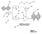
- a low power modulated signal 200 is input to the system 100 at point 110.
- the modulated signal 200 is both phase modulated (PM) and amplitude modulated (AM).
- the signal is split using a splitter 120 into two equal components.
- the first component is applied to detector 130 which outputs a signal corresponding to the envelope 210 of the signal 200.
- Signal 210 therefore corresponds to the AM information in the signal 200.
- the second signal is applied to limiter 140 which outputs a hard limited version 220 of the signal 200.
- Signal 220 has all the amplitude variation removed from it, and therefore corresponds to the PM information in the signal 200.
- the detected signal 210 is applied to amplifier 150, which is used to drive the power supply to the power amplifier 160.
- the power amplifier 160 can operate with a constant gain, and the variation in the envelope of the input signal 200 can be recreated by altering the power supply in sympathy with the envelope of input signal 200, as represented by signal 210.
- the resultant output signal 230 corresponds to an amplified version of the input signal 200, and is ready for transmission by an antenna (not shown).
- f t g t . e jh t
- the output signal 230 is given by F(t), and is an amplified version of f(t).
- a transmitter comprising: a processor for generating digital phase and digital amplitude signals which characterise an input digital data stream: a signal generator for generating an RF carrier signal with a phase property defined by the generated digital phase signal; an amplifier arranged to receive the RF carrier signal as an input; and a bi-level switching circuit responsive to the generated digital amplitude signal to switch between a first voltage level and a second voltage level to generate a voltage signal for supplying power to the amplifier.
- a method comprising: generating, from an input digital data stream, a digital phase signal and a digital amplitude signal which characterise the digital data stream; generating an RF carrier signal having a phase property defined by the digital phase signal; passing the RF carrier signal to an RF amplifier; causing, in response to the digital amplitude signal, a bi-level switching circuit to switch between a first voltage level and a second voltage level to generate a voltage supply signal; and applying the voltage supply signal to a power supply input of the amplifier.
- the switching circuit operates to supply a signal which is switched between two voltage supply rails. There are two possible outputs - each equivalent to a voltage rail. In practice, the values will differ slightly due to internal resistances in the active devices forming the switching circuitry. Such switching offers power efficiency savings.
- a transmitter using an amplifier according to embodiments of the invention is able to accept purely digital inputs.
- the digital inputs need only represent the data to be transmitted in a suitable format for modulation,
- the modulation process itself occurs in the PA when the phase and amplitude information are effectively re-combined,
- the ability to operate almost exclusively in the digital domain offers well known advantages in the area of circuit design and layout.
- a transmitter according to embodiments of the invention is operable in combination with a wide range of modulation schemes.
- Different communication standards prescribe different modulation schemes for use by devices operating according to each standard.
- Embodiments of the invention are able to be used with different modulation schemes due to the manner in which amplitude and phase modulation are achieved.
- GMSK modulation scheme This scheme is known as constant-amplitude as the envelope of the transmitted signal does not alter.
- the information is encoded in the phase variation of the modulated signal.
- W-CDMA Wideband CDMA
- Embodiments of the invention may be considered as universal transmitters/modulators, as the exact modulation scheme can be determined in the software which is used to derive the input signals to the transmitter. The hardware of the transmitter itself does not change.
- embodiments of the invention do not require the production of In-phase (I) and Quadrature-phase (Q) components to generate the modulated signal. This leads to savings in component count, and a consequential power saving.
- Embodiments of the invention preferably utilise a pair of signals to represent the data to be transmitted.
- the pair of signals includes a signal representing the phase of the data signal, and a signal representing the amplitude of the data signal.
- the amplitude signal is not a direct representation of the desired resultant envelope of the RF signal. Rather, it is a digitally coded signal which is used to switch an efficient switching amplifier or modulator.
- the output of the switching amplifier or modulator then provides the voltage supply to an RF power amplifier, which is in turn fed by an RF carrier signal which has been phase modulated in accordance with the digital signal representing the phase of the input signal.
- Embodiments of the invention utilise digital data representing the data to be transmitted to control the operation of the PA. Such operation allows the PA to effectively act as a modulator, as this is the first point in the transmit chain where a signal having the phase and amplitude characteristics of the final transmitted signal exists.
- embodiments of the invention enjoy substantially higher efficiencies than prior art devices. Improvements of up to 30 or 40 percentage points are possible over prior art devices. Since some prior art devices are only 45% efficient, the available battery life may be nearly double that previously attainable.
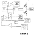
- FIG. 2 shows a transmitter 300 according to an embodiment of the invention.
- the transmitter has an input 310 for receiving a digital data stream representing the data to be transmitted.
- the data as this point has been coded and formatted as required by the particular communication standard to be used for that transmission. For example, if the transmission is to be according to GSM, then certain coding of the speech will have been performed, the data will have had error-correction and error-detection bits added, and interleaving of the data over successive frames will have been performed.
- the same raw, e.g. speech, data to be transmitted according to other communication standards will have been processed in a manner required by that particular standard.
- the data input at 310 is processed by some form of microprocessor 320 such as a Digital Signal Processor (DSP).
- the microprocessor 320 produces two output signals.
- the first signal 330 represents the amplitude of the data to be transmitted.
- the second signal 340 represents the phase of the data to be transmitted.
- These two signals can be generated in such a way, by software in the microprocessor, that any modulation scheme relying on phase and/or amplitude modulation can be effected using the transmitter 300.
- the transmitter 300 can be considered as a universal transmitter i.e. usable with a wide range of differing communication protocols.
- the phase signal 340 is mixed with a signal 370 at the frequency of transmission in mixer 360.
- the resultant signal forms the input to power amplifier 380.
- the phase signal 340 can take a different format and can be used to control a frequency synthesiser (not shown) to generate a signal which forms the input to power amplifier 380. In either case, the phase varying component of the resultant signal is derived from the signal 340.
- the PA 380 amplifies its input signal to produce RF output signal 400 which is then ready for transmission.
- the signal will probably be routed via one or more filters before reaching an antenna.
- the amplitude signal 330 derived from the digital input signal 310, is used to generate a voltage supply signal 390 for the PA.
- This voltage supply signal 390 is made to alter in sympathy with the desired envelope of the RF output signal 400. In this way, the notional gain of the PA remains constant, and the time-varying envelope of the resultant signal is achieved by altering the voltage applied to the PA 380.
- the exact relationship between the derived amplitude signal 330 and the digital input signal 310 is determined empirically for each type of modulation supported. In practice, history data, i.e. data occurring prior to a given present time, may be used to generate the digital signal 330.
- a perfect digital pulse, i.e. one having perfect edges, in the frequency domain corresponds to a pulse in the time domain having infinite pulse width as the tails of the waveform decay.
- the time domain representation must be truncated. The point at which the waveform is truncated can be determined by several factors, such as the processing power available or the size of look up table used to hold history data.
- the net effect of truncation is that the current value of data under consideration can only have been derived from a finite number of previous values. For instance, if T is the symbol/bit period, and you decide to truncate at 4T, then the history, i.e. the impact of the previous data bits on the current data bit lasts for 4T. This means that the tails of the waveforms of the previous 3 bits are superimposed onto the current bit, and there are 2 4 possibilities for each bit.
- the digital signal 330 can be calculated from a look up table of history data and knowing the current bit value. Different modulation schemes will each produce a differently structured signal 330.
- the signal 330 takes the form of a pulse width modulated (PWM) signal.
- PWM pulse width modulated
- Such a signal has a time-varying duty cycle, and can be used to control a switch 350 which supplies power to the power amplifier 380.
- a suitable form for the switch 350 may be a switching modulator - a so-called s-class modulator.
- a switching modulator or amplifier offers efficiency advantages over certain other forms of modulator or amplifier.
- a particularly preferred embodiment uses a form of switching circuit termed an 'H-Bridge' to generate the voltage supply signal 390 to the PA 380.
- the H-Bridge 500 itself comprises 4 switching elements 530, 540, 550, 560, preferably transistors having a low 'on' resistance.
- Field Effect Transistors (FETs) are particularly suitable for this task.
- the transistors are arranged in pairs, and by controlling which pair is on at any given time, it is possible to create a pseudo-digital waveform which varies between two voltage extremes.
- Such a scheme requires two control signals 510, 520. It is instructive to consider one of the control signals to be a signal which controls the 'charging' of the PA. The other signal controls the 'discharging' of the PA. By using two signals in this way, as opposed to using a single control signal to switch the PA on and off, it is possible to achieve even greater energy efficiency. This is because the PA is not allowed to decay naturally after it has been 'charged' - such decay wastes energy. Rather, it is forced to 'discharge' by the second control signal, ensuring that energy is not wasted by the decay process.
- the charging and discharging signals can be understood to be analogous to the accelerator and brake pedal found in cars. The brake ensures that the response does not merely decay, but decelerates as required.
- the two control signals 510 and 520 which replace the single control signal 330 of Figure 2 , are received in the H-Bridge 500 by decoder 570.
- the decoder is operable to generate control signals to switch the pairs of transistors 540 & 550, 530 & 560.
- the transistors in each pair are always operated together, as indicated by the control signals emanating from decoder 570.
- the dotted lines connected to 540 and 550 represent signals which are identical, as do the dashed lines connected to 530 and 560.
- the output from switching circuit 350 consists of a square wave signal with stable values at two fixed points - +V and -V (or GND). In the embodiment featuring the H-Bridge, the outputs are similar.
- Such a switched output signal provides an efficient mode of operation for switching circuit 350 which contributes to the overall power efficiency of the transmitter.
- the outputs from the H-Bridge are shown feeding into an envelope reconstruction filter 580.
- the filter's role is to eliminate sampling noise from the H-Bridge outputs, and output smoothed AM signals 590 and 595 to supply power to the PA's two power rails.
- signals 590 and 595 replace signal 390 of Figure 2 .
- Prior art PAs tended to operate in a linear fashion, which, as described, can be very inefficient. Since the amplitude of the signal 400 from the PA is controlled by signal 390, rather than varying the gain of the PA, the PA can be made to operate in a switched mode, resulting in power efficiency gains also.
- the RF input to the PA can be allowed overdrive the PA, i.e. allow it to operate in saturated mode, effectively as a switch, safe in the knowledge that the amplitude information which forms part of the encoded signal is impressed upon the final signal 400 by the varying voltage supply 390 which is fed to the PA.
- the present invention includes any novel feature or combination of features disclosed herein either explicitly or any generalisation thereof irrespective of whether or not it relates to the claimed invention or mitigates any or all of the problems addressed.
- High efficiency PA module integrated with a continuously-variable-power-supply (MEG algorithm), efficiency management system solution.
- MEG algorithm continuously-variable-power-supply
- HEPA High Efficiency Power Amplifiers
- W-CDMA wide band code division, multiple access
- GSM EDGE GSM EDGE
- the power added efficiencies for these modulation schemes have been reported in the 20-percentile range, due to the large amplitude modulation component. This significantly increases battery current consumption which, would decreases talk time of these phones compared to other past generations of digital modulation systems.
- the challenge is to generate the amplitude modulation very efficiently in a wide video bandwidth.
- the video amplifier efficiency needed to effectively recover talk time, must be above 80%.
- Amplifier modulation performance must be very linear and noise free. Normally, linearity and efficiency together are not possible using conventional linear design techniques. The efficiency results from such a linear video amplifier would be in the low 20-percentile range. A large heatsink would be required with this kind of design degrading the requirement to keep the weight down of the hand held phone. Cost would also be increased because of the larger battery required to meet the talk time.
- Envelope tracking DC to DC converters, power DAC and class AB push pull video amplifier are some of the methods used to amplify the amplitude signal.
- a single amplifier could be used with class "A" operation to achieve the lowest distortion. This is the least efficient method to transfer of the amplitude energy to the RF amplifier.
- envelope tracking was used to make slow corrections to the DC supply only and would be unstable if modulated at the WCDMA chip rate.
- Envelope tracking DC to DC converter output adjusting the sense, voltage loop, gain to reproduce the AM low bit rate modulation power.
- Device Fmax (see note 1) limited control, loop, bandwidth hence the modulation rate cannot be exceed without distortion or stability problems.
- DC to DC tracking converters In some DC to DC tracking converters the efficiency falls as the load current decreases. This is not satisfactory for optimal system efficiency of our modulation restoration technique as there is a power out control specification. Also DC converters may require a large, ferrite, core, inductor to convert the switched energy to envelop power.
- the ferrite core limits the bandwidth and control word response due to the natural hysteresis and bandpass characteristics of the iron material.
- PDAC Power digital to analogue converters
- Analog to digital solutions convert energy more efficiently using several pulse formats.
- the envelope could be converted to pulse-width; pulse-amplitude; pulse-density; pulse-position or a combination of all is also possible.
- Most of the applications are designed for audio amplifier bandwidths.
- the final application requires transferring energy directly to the RF amplifier. Final power transfer may require class-AB or class-A amplification after the digital processing. This completes the waveform superposition of phase and amplitude data (waveform restoration).
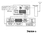
- the baseband chip generates the initial amplitude signal.
- This signal is converted to a bipolar stream using any of the above formats. (Pulse density is believed to be the most efficient method).
- the method simply increases the pulse repetition rate with the envelope peaks and troughs. Polarity, plus or minus, of the pulse determines peaks or trough of the envelope.
- a DAC capable of transforming the amplitude energy in this format is known as a sigma delta technique.
- One limitation with this method is the analogue is required to be over sampled by a one bit quantisation process (20 times is typical). This produces out of band switch noise.
- linear amplification technique requires very little explanation. It may be a very specialised amplifier design as it is required to work with very wide linear gain and phase bandwidth capable of passing the amplitude modulation product and its harmonic components which, are essential for the restoration process to work.
- the linear phase and gain bandwidth needs to be at least 3 times the 3.84Mbit chip rate at high drive currents. This is a very difficult engineering task fraught with compromises.
- Baseband computes the amount of energy need by the PA from a matrix and encodes it as a binary stream MEG1.
- the baseband also computes the energy requires to discharge the PA and is encoded in a second binary stream (MEG-2).
- the energy management circuit is mounted on the PA package.
- the MEG binary signals and the energy management solution are equivalent to a continuously variable power supply for the PA at the chip rate. Efficiency is kept constant at all voltage levels of the energy manager circuit during amplitude modulation of the PA.
- Phase modulated RF power is amplified using the most efficient saturated RF amplifier techniques. This requires the latest RF device technology with at least 40 GHz Fmax.
- the energy manager is connected to the battery provides the power supply to the PA.
- a filter between the energy manager and the PA is used as a reconstruction filter for the digital AM signal.
- simultaneous waveform restoration technique cancels the broadband spectrum generated by the phase modulation.
- the combined application of the digital energy manager, MEG and saturated PA results in high efficiency compliant to the air interface specifications.
- An algorithm solution, adapting the MEG binary code to AM energy in the digital manager, is all that is required to control the RF power output dynamic range.
- the PA system solution is achieved for all modulation formats by adaptation of the MEG's bit patterns.
- Integration of the PA with the energy manager eliminates a power dissipative path on the PCB. This reduces 2R dissipation to the PA and filter as they are in the same (package) location.
- Drive (MEG) to the energy manager is through high impedance lines. This helps to reduce radiation of the MEG signal and interfering with the frequency plan of the phone.
- the direct generation of the binary MEG codes to the energy manager can be derived closer to the source of modulation generation.
- I.E. The system does not need to access modulation digital formats of IQ and convert them. DSP power over-heads are reduced and bandwidth is reduced generating the MEG binary format compared to encoding the bipolar power density signal from a Sigma Delta modulation process.
- the MEG modulation technique has a specific new algorithm design.
- Hardware is under construction to demonstrate the technique and train the MEG.
- An AO is in the process of approval.
Landscapes
- Engineering & Computer Science (AREA)
- Power Engineering (AREA)
- Computer Networks & Wireless Communication (AREA)
- Signal Processing (AREA)
- Amplifiers (AREA)
- Amplitude Modulation (AREA)
- Transmitters (AREA)
- Digital Transmission Methods That Use Modulated Carrier Waves (AREA)
Claims (25)
- Sender umfassend:einen Prozessor zum Erzeugen digitaler Phasen- und digitaler Amplitudensignale, die einen digitalen Eingangsdatenstrom kennzeichnen,einen Signalerzeuger zum Erzeugen eines Funkfrequenz-Trägersignals mit einer Phaseneigenschaft, die durch das erzeugte digitale Phasensignal definiert ist,einen Verstärker der eingerichtet ist, das Funkfrequenz-Trägersignal als eine Eingabe zu empfangen, undeinen Zweiniveau-Schaltkreis, der auf das erzeugte digitale Amplitudensignal anspricht, um zwischen einem ersten Spannungsniveau und einem zweiten Spannungsniveau zu schalten, um ein Spannungssignal zu erzeugen um den Verstärker mit Strom zu versorgen.
- Sender gemäß Anspruch 1, wobei der Schaltkreis eine H-Brückenschaltung ist.
- Sender gemäß einem der vorstehenden Ansprüche, wobei das digitale Amplitudensignal mehrere codierte Datenströme zum Steuern des Schaltkreises umfasst.
- Sender gemäß Anspruch 3, wobei die mehreren codierten Datenströme einen ersten Strom zum Steuern des Ladens des Verstärkers, und einen zweiten Strom zum Steuern des Entladens des Verstärkers umfassen.
- Sender gemäß einem der vorstehenden Ansprüche, wobei das digitale Amplitudensignal ein pulsweitenmoduliertes (PWM) Signal ist.
- Sender gemäß einem der vorstehenden Ansprüche, wobei das erzeugte digitale Amplitudensignal nur Amplitudeninformation umfasst.
- Sender gemäß einem der vorstehenden Ansprüche, wobei das erzeugte digitale Phasensignal nur Phaseninformation umfasst.
- Sender gemäß einem der vorstehenden Ansprüche, wobei der Verstärkter eingerichtet ist, um in einem geschalteten Modus zu arbeiten.
- Sender gemäß einem der vorstehenden Ansprüche, wobei der Signalerzeuger ein Frequenz-Synthetisierer ist.
- Sender gemäß einem der vorstehenden Ansprüche, wobei der Schaltkreis an seinem Ausgang einen Rekonstruktionsfilter aufweist.
- Sender gemäß einem der vorstehenden Ansprüche, wobei der Prozessor zum Erzeugen der digitalen Phaseninformation eine Phasenmaschine ist.
- Sender gemäß einem der vorstehenden Ansprüche, wobei der Prozessor zum Erzeugen der digitalen Amplitudeninformation eine Amplitudenmaschine ist.
- Sender gemäß einem der vorstehenden Ansprüche, wobei das digitale Amplitudensignal ein MEG- (Modulation Energy Gain) Signal ist.
- Verfahren, umfassend:Erzeugen aus einem digitalen Eingangsdatenstrom, eines digitalen Phasensignals und eines digitalen Amplitudensignals, die den digitalen Eingangsdatenstrom kennzeichnen,Erzeugen eines Funkfrequenz-Trägersignals mit einer Phaseneigenschaft, die durch das digitale Phasensignal definiert ist,Weitergeben des Funkfrequenz-Trägersignals an einen Funkfrequenz-Verstärker, und Veranlassen eines Zweiniveau-Schaltkreis, in Reaktion auf das digitale Amplitudensignal, zwischen einem ersten Spannungsniveau und einem zweiten Spannungsniveau zu schalten, um ein Spannungsversorgungssignal zu erzeugen, und Anlegen des Spannungsversorgungssignals an einen Spannungsversorgungseingang des Verstärkers.
- Verfahren gemäß Anspruch 14, wobei der Schaltkreis eine H-Brückenschaltung ist.
- Verfahren gemäß einem der Ansprüche 14 oder 15, wobei das digitale Amplitudensignal mehrere codierte Datenströme zum Steuern des Schaltkreises umfasst.
- Verfahren gemäß Anspruch 16, wobei die mehreren codierten Datenströme einen ersten Strom zum Steuern des Ladens des Verstärkers und einen zweiten Strom zum Steuern des Entladens des Verstärkers umfassen.
- Verfahren gemäß einem der Ansprüche 14 bis 17, wobei das digitale Amplitudensignal ein pulsweitenmoduliertes (PWM) Signal ist.
- Verfahren gemäß einem der Ansprüche 14 bis 18, wobei das erzeugte digitale Amplitudensignal nur Amplitudeninformation umfasst.
- Verfahren gemäß einem der Ansprüche 14 bis 19, wobei der Verstärker eingerichtet ist, um in einem geschalteten Modus zu arbeiten.
- Verfahren gemäß einem der Ansprüche 14 bis 20, wobei die Erzeugung des Funkfrequenz-Trägersignals durch einen Frequenz-Synthetisierer durchgeführt wird.
- Verfahren gemäß einem der Ansprüche 14 bis 21, wobei der Schaltkreis an seinem Ausgang einen Rekonstruktionsfilter aufweist.
- Verfahren gemäß einem der Ansprüche 14 bis 22, wobei die Erzeugung der digitalen Phaseninformation durch eine Phasenmaschine durchgeführt wird.
- Verfahren gemäß einem der Ansprüche 14 bis 23, wobei die Erzeugung der digitalen Amplitudeninformation durch eine Amplitudenmaschine durchgeführt wird.
- Verfahren gemäß einem der Ansprüche 14 bis 24, wobei das digitale Amplitudensignal ein MEG- (Modulation Energy Gain) Signal ist.
Applications Claiming Priority (3)
| Application Number | Priority Date | Filing Date | Title |
|---|---|---|---|
| GBGB0014344.6A GB0014344D0 (en) | 2000-06-13 | 2000-06-13 | Universal modulation mode tri-amplifier |
| GB0014344 | 2000-06-13 | ||
| PCT/EP2001/007055 WO2001097479A1 (en) | 2000-06-13 | 2001-06-13 | Method and apparatus for modulating a radio signal using digital amplitude and phase control signals |
Publications (2)
| Publication Number | Publication Date |
|---|---|
| EP1293074A1 EP1293074A1 (de) | 2003-03-19 |
| EP1293074B1 true EP1293074B1 (de) | 2009-11-11 |
Family
ID=9893493
Family Applications (1)
| Application Number | Title | Priority Date | Filing Date |
|---|---|---|---|
| EP01951622A Expired - Lifetime EP1293074B1 (de) | 2000-06-13 | 2001-06-13 | Verfahren und vorrichtung zum modulieren eines rundfunksignals unter verwendung digitalen amplituden- und phasen-steuerungssignale |
Country Status (8)
| Country | Link |
|---|---|
| US (1) | US7657238B2 (de) |
| EP (1) | EP1293074B1 (de) |
| CN (1) | CN1214587C (de) |
| AT (1) | ATE448621T1 (de) |
| AU (1) | AU2001272501A1 (de) |
| DE (1) | DE60140444D1 (de) |
| GB (1) | GB0014344D0 (de) |
| WO (1) | WO2001097479A1 (de) |
Families Citing this family (16)
| Publication number | Priority date | Publication date | Assignee | Title |
|---|---|---|---|---|
| US7409004B2 (en) * | 2001-06-19 | 2008-08-05 | Matsushita Electric Industrial Co., Ltd. | Hybrid polar modulator differential phase Cartesian feedback correction circuit for power amplifier linearization |
| US7502422B2 (en) | 2003-06-04 | 2009-03-10 | M/A—COM, Inc. | Electromagnetic wave transmitter systems, methods and articles of manufacture |
| AU2003275475A1 (en) * | 2002-10-08 | 2004-05-04 | M/A-Com, Inc. | Transmitter and methods of transmission using separate phase and amplitude modulators |
| US7372333B2 (en) | 2003-02-03 | 2008-05-13 | Arizona Board Of Regents, Acting For And On Behalf Of Arizona State University | Monolithic supply-modulated RF power amplifier and DC-DC power converter IC |
| US7042958B2 (en) * | 2003-06-04 | 2006-05-09 | Tropian, Inc. | Digital time alignment in a polar modulator |
| US8031028B2 (en) * | 2004-07-07 | 2011-10-04 | SiGe Semiconductor (Europe) Ltd. | Polar signal processor to drive a segmented power amplifier and method therefore |
| US7983632B2 (en) * | 2004-09-24 | 2011-07-19 | Broadcom Corporation | Feedback control loop for amplitude modulation in a polar transmitter with a translational loop |
| US20070015472A1 (en) * | 2005-07-15 | 2007-01-18 | Simo Murtojarvi | Multimode transmitter, module, communication device and chip set |
| JP5003134B2 (ja) * | 2006-01-10 | 2012-08-15 | 日本電気株式会社 | 増幅装置 |
| ES2374220T3 (es) * | 2006-06-27 | 2012-02-14 | Telefonaktiebolaget Lm Ericsson (Publ) | Amplificación de potencia en modo conmutado. |
| GB2496379A (en) * | 2011-11-04 | 2013-05-15 | Univ Edinburgh | A freespace optical communication system which exploits the rolling shutter mechanism of a CMOS camera |
| US8854127B2 (en) * | 2012-05-15 | 2014-10-07 | Intel Mobile Communications GmbH | DC-DC converter for envelope tracking |
| JP2014082749A (ja) * | 2012-09-28 | 2014-05-08 | Fordan Kk | 複合電力増幅器を有する複合送信機 |
| CN111064691B (zh) * | 2016-01-27 | 2024-02-09 | 华为技术有限公司 | 发射机、接收机和信号处理的方法 |
| US9503294B1 (en) * | 2016-06-14 | 2016-11-22 | Northrop Grumman Systems Corporation | Amplitude and phase shift keying modulation for saturated amplifier systems |
| FR3099010B1 (fr) * | 2019-07-15 | 2021-08-06 | Commissariat Energie Atomique | Émetteur uwb compact à très basse consommation et forme d’onde reconfigurable |
Family Cites Families (16)
| Publication number | Priority date | Publication date | Assignee | Title |
|---|---|---|---|---|
| US4724396A (en) * | 1984-08-21 | 1988-02-09 | Peavey Electronics Corporation | Digital audio amplifier |
| US4916599A (en) * | 1989-03-29 | 1990-04-10 | Hyperpower, Inc. | Switching power supply |
| US5430416A (en) * | 1994-02-23 | 1995-07-04 | Motorola | Power amplifier having nested amplitude modulation controller and phase modulation controller |
| FR2758024B1 (fr) * | 1996-12-30 | 1999-01-29 | Alsthom Cge Alcatel | Dispositif d'alimentation d'un amplificateur de puissance pour terminal de radiocommunications mobiles |
| KR100241780B1 (ko) * | 1997-12-16 | 2000-02-01 | 윤종용 | 무선 통신 단말기의 전원 절약 장치 |
| FI105609B (fi) | 1998-10-27 | 2000-09-15 | Nokia Mobile Phones Ltd | Menetelmä ja järjestely lähetyssignaalin muodostamiseksi |
| EP1035701A1 (de) | 1999-03-08 | 2000-09-13 | Motorola, Inc. | Modulator, der Einhüllendenbeseitigung und -Wiederherstellung mittels Nachschlagtabellen verwendet |
| JP3822057B2 (ja) * | 1999-04-02 | 2006-09-13 | 三菱電機株式会社 | 移動通信端末装置 |
| EP1056248A1 (de) | 1999-05-26 | 2000-11-29 | Ascom AG | Modulator, der getrennte Stufen für Phase und Amplitude verwendet |
| US6127816A (en) * | 1999-08-04 | 2000-10-03 | Hewlett-Packard Company | Multiple frequency switching power supply and methods to operate a switching power supply |
| US6462971B1 (en) * | 1999-09-24 | 2002-10-08 | Power Integrations, Inc. | Method and apparatus providing a multi-function terminal for a power supply controller |
| US6449465B1 (en) * | 1999-12-20 | 2002-09-10 | Motorola, Inc. | Method and apparatus for linear amplification of a radio frequency signal |
| US6366177B1 (en) * | 2000-02-02 | 2002-04-02 | Tropian Inc. | High-efficiency power modulators |
| US6452366B1 (en) * | 2000-02-11 | 2002-09-17 | Champion Microelectronic Corp. | Low power mode and feedback arrangement for a switching power converter |
| US6229289B1 (en) * | 2000-02-25 | 2001-05-08 | Cadence Design Systems, Inc. | Power converter mode transitioning method and apparatus |
| US6721368B1 (en) * | 2000-03-04 | 2004-04-13 | Qualcomm Incorporated | Transmitter architectures for communications systems |
-
2000
- 2000-06-13 GB GBGB0014344.6A patent/GB0014344D0/en not_active Ceased
-
2001
- 2001-06-13 DE DE60140444T patent/DE60140444D1/de not_active Expired - Lifetime
- 2001-06-13 CN CN01813812.8A patent/CN1214587C/zh not_active Expired - Lifetime
- 2001-06-13 EP EP01951622A patent/EP1293074B1/de not_active Expired - Lifetime
- 2001-06-13 AT AT01951622T patent/ATE448621T1/de not_active IP Right Cessation
- 2001-06-13 US US10/297,847 patent/US7657238B2/en not_active Expired - Lifetime
- 2001-06-13 AU AU2001272501A patent/AU2001272501A1/en not_active Abandoned
- 2001-06-13 WO PCT/EP2001/007055 patent/WO2001097479A1/en not_active Ceased
Also Published As
| Publication number | Publication date |
|---|---|
| ATE448621T1 (de) | 2009-11-15 |
| US20040046607A1 (en) | 2004-03-11 |
| GB0014344D0 (en) | 2000-08-02 |
| EP1293074A1 (de) | 2003-03-19 |
| WO2001097479A1 (en) | 2001-12-20 |
| US7657238B2 (en) | 2010-02-02 |
| CN1214587C (zh) | 2005-08-10 |
| CN1446424A (zh) | 2003-10-01 |
| AU2001272501A1 (en) | 2001-12-24 |
| DE60140444D1 (de) | 2009-12-24 |
Similar Documents
| Publication | Publication Date | Title |
|---|---|---|
| EP1293074B1 (de) | Verfahren und vorrichtung zum modulieren eines rundfunksignals unter verwendung digitalen amplituden- und phasen-steuerungssignale | |
| EP1536556B1 (de) | Schaltverstärkerarchitektur | |
| US7043213B2 (en) | Multi-mode amplifier system | |
| US7042287B2 (en) | System and method for reducing dynamic range and improving linearity in an amplication system | |
| CN105684301B (zh) | 功率编码器和用于对数据进行调制的方法 | |
| US20070014382A1 (en) | Reconfigurable transmitter | |
| JP2005020693A (ja) | 極および線形増幅器システム | |
| US20090273396A1 (en) | Pulse Area Modulation and High-Efficiency Linear Power Amplifier System Using the Same | |
| EP2005602A1 (de) | Multimodale funksender und betriebsverfahren dafür | |
| WO2002075918A2 (en) | Modulator using class-e stage | |
| EP3028387B1 (de) | Auf einem pegeldemultiplexierenden delta-sigma modulator basierenden sender | |
| KR100810322B1 (ko) | 이동 통신용 고효율 전력 증폭 장치 및 방법 | |
| US8335250B2 (en) | Multi-level pulse width modulation power amplifier method and apparatus | |
| US8054878B2 (en) | Apparatus and method for amplifying signal power in a communication system | |
| WO2010011606A1 (en) | Signal decomposition methods and apparatus for multi-mode transmitters | |
| CN101167326A (zh) | 极化调制传输电路和通信设备 | |
| US6300830B1 (en) | Multiplexed input envelope restoration scheme for linear high-efficiency power amplification | |
| Li et al. | High average-efficiency multimode RF transmitter using a hybrid quadrature polar modulator | |
| CN101087147A (zh) | 发射机及其基频处理器与射频功率放大器的调制方法 | |
| US10652057B1 (en) | All digital outphasing transmitter | |
| Jau et al. | Polar modulation-based RF power amplifiers with enhanced envelope processing technique | |
| Kim et al. | Digitally enhanced linear power amplifiers |
Legal Events
| Date | Code | Title | Description |
|---|---|---|---|
| PUAI | Public reference made under article 153(3) epc to a published international application that has entered the european phase |
Free format text: ORIGINAL CODE: 0009012 |
|
| 17P | Request for examination filed |
Effective date: 20030113 |
|
| AK | Designated contracting states |
Kind code of ref document: A1 Designated state(s): AT BE CH CY DE DK ES FI FR GB GR IE IT LI LU MC NL PT SE TR |
|
| AX | Request for extension of the european patent |
Extension state: AL LT LV MK RO SI |
|
| 17Q | First examination report despatched |
Effective date: 20061124 |
|
| GRAP | Despatch of communication of intention to grant a patent |
Free format text: ORIGINAL CODE: EPIDOSNIGR1 |
|
| GRAS | Grant fee paid |
Free format text: ORIGINAL CODE: EPIDOSNIGR3 |
|
| GRAA | (expected) grant |
Free format text: ORIGINAL CODE: 0009210 |
|
| AK | Designated contracting states |
Kind code of ref document: B1 Designated state(s): AT BE CH CY DE DK ES FI FR GB GR IE IT LI LU MC NL PT SE TR |
|
| REG | Reference to a national code |
Ref country code: GB Ref legal event code: FG4D |
|
| REG | Reference to a national code |
Ref country code: CH Ref legal event code: EP |
|
| REG | Reference to a national code |
Ref country code: IE Ref legal event code: FG4D |
|
| REF | Corresponds to: |
Ref document number: 60140444 Country of ref document: DE Date of ref document: 20091224 Kind code of ref document: P |
|
| NLV1 | Nl: lapsed or annulled due to failure to fulfill the requirements of art. 29p and 29m of the patents act | ||
| PG25 | Lapsed in a contracting state [announced via postgrant information from national office to epo] |
Ref country code: PT Free format text: LAPSE BECAUSE OF FAILURE TO SUBMIT A TRANSLATION OF THE DESCRIPTION OR TO PAY THE FEE WITHIN THE PRESCRIBED TIME-LIMIT Effective date: 20100311 Ref country code: ES Free format text: LAPSE BECAUSE OF FAILURE TO SUBMIT A TRANSLATION OF THE DESCRIPTION OR TO PAY THE FEE WITHIN THE PRESCRIBED TIME-LIMIT Effective date: 20100222 Ref country code: SE Free format text: LAPSE BECAUSE OF FAILURE TO SUBMIT A TRANSLATION OF THE DESCRIPTION OR TO PAY THE FEE WITHIN THE PRESCRIBED TIME-LIMIT Effective date: 20091111 Ref country code: FI Free format text: LAPSE BECAUSE OF FAILURE TO SUBMIT A TRANSLATION OF THE DESCRIPTION OR TO PAY THE FEE WITHIN THE PRESCRIBED TIME-LIMIT Effective date: 20091111 |
|
| PG25 | Lapsed in a contracting state [announced via postgrant information from national office to epo] |
Ref country code: CY Free format text: LAPSE BECAUSE OF FAILURE TO SUBMIT A TRANSLATION OF THE DESCRIPTION OR TO PAY THE FEE WITHIN THE PRESCRIBED TIME-LIMIT Effective date: 20091111 |
|
| PG25 | Lapsed in a contracting state [announced via postgrant information from national office to epo] |
Ref country code: BE Free format text: LAPSE BECAUSE OF FAILURE TO SUBMIT A TRANSLATION OF THE DESCRIPTION OR TO PAY THE FEE WITHIN THE PRESCRIBED TIME-LIMIT Effective date: 20091111 Ref country code: AT Free format text: LAPSE BECAUSE OF FAILURE TO SUBMIT A TRANSLATION OF THE DESCRIPTION OR TO PAY THE FEE WITHIN THE PRESCRIBED TIME-LIMIT Effective date: 20091111 |
|
| PG25 | Lapsed in a contracting state [announced via postgrant information from national office to epo] |
Ref country code: DK Free format text: LAPSE BECAUSE OF FAILURE TO SUBMIT A TRANSLATION OF THE DESCRIPTION OR TO PAY THE FEE WITHIN THE PRESCRIBED TIME-LIMIT Effective date: 20091111 |
|
| PLBE | No opposition filed within time limit |
Free format text: ORIGINAL CODE: 0009261 |
|
| STAA | Information on the status of an ep patent application or granted ep patent |
Free format text: STATUS: NO OPPOSITION FILED WITHIN TIME LIMIT |
|
| 26N | No opposition filed |
Effective date: 20100812 |
|
| PG25 | Lapsed in a contracting state [announced via postgrant information from national office to epo] |
Ref country code: GR Free format text: LAPSE BECAUSE OF FAILURE TO SUBMIT A TRANSLATION OF THE DESCRIPTION OR TO PAY THE FEE WITHIN THE PRESCRIBED TIME-LIMIT Effective date: 20100212 |
|
| PG25 | Lapsed in a contracting state [announced via postgrant information from national office to epo] |
Ref country code: MC Free format text: LAPSE BECAUSE OF NON-PAYMENT OF DUE FEES Effective date: 20100630 |
|
| REG | Reference to a national code |
Ref country code: CH Ref legal event code: PL |
|
| REG | Reference to a national code |
Ref country code: FR Ref legal event code: ST Effective date: 20110228 |
|
| PG25 | Lapsed in a contracting state [announced via postgrant information from national office to epo] |
Ref country code: IT Free format text: LAPSE BECAUSE OF FAILURE TO SUBMIT A TRANSLATION OF THE DESCRIPTION OR TO PAY THE FEE WITHIN THE PRESCRIBED TIME-LIMIT Effective date: 20091111 |
|
| PG25 | Lapsed in a contracting state [announced via postgrant information from national office to epo] |
Ref country code: IE Free format text: LAPSE BECAUSE OF NON-PAYMENT OF DUE FEES Effective date: 20100613 Ref country code: CH Free format text: LAPSE BECAUSE OF NON-PAYMENT OF DUE FEES Effective date: 20100630 Ref country code: LI Free format text: LAPSE BECAUSE OF NON-PAYMENT OF DUE FEES Effective date: 20100630 |
|
| PG25 | Lapsed in a contracting state [announced via postgrant information from national office to epo] |
Ref country code: FR Free format text: LAPSE BECAUSE OF NON-PAYMENT OF DUE FEES Effective date: 20100630 |
|
| PG25 | Lapsed in a contracting state [announced via postgrant information from national office to epo] |
Ref country code: LU Free format text: LAPSE BECAUSE OF NON-PAYMENT OF DUE FEES Effective date: 20100613 Ref country code: NL Free format text: LAPSE BECAUSE OF FAILURE TO SUBMIT A TRANSLATION OF THE DESCRIPTION OR TO PAY THE FEE WITHIN THE PRESCRIBED TIME-LIMIT Effective date: 20091111 |
|
| PG25 | Lapsed in a contracting state [announced via postgrant information from national office to epo] |
Ref country code: TR Free format text: LAPSE BECAUSE OF FAILURE TO SUBMIT A TRANSLATION OF THE DESCRIPTION OR TO PAY THE FEE WITHIN THE PRESCRIBED TIME-LIMIT Effective date: 20091111 |
|
| REG | Reference to a national code |
Ref country code: GB Ref legal event code: 732E Free format text: REGISTERED BETWEEN 20150910 AND 20150916 |
|
| REG | Reference to a national code |
Ref country code: DE Ref legal event code: R081 Ref document number: 60140444 Country of ref document: DE Owner name: NOKIA TECHNOLOGIES OY, FI Free format text: FORMER OWNER: NOKIA CORP., 02610 ESPOO, FI |
|
| REG | Reference to a national code |
Ref country code: GB Ref legal event code: 732E Free format text: REGISTERED BETWEEN 20190124 AND 20190130 |
|
| REG | Reference to a national code |
Ref country code: DE Ref legal event code: R081 Ref document number: 60140444 Country of ref document: DE Owner name: PROVENANCE ASSET GROUP LLC, PITTSFORD, US Free format text: FORMER OWNER: NOKIA TECHNOLOGIES OY, ESPOO, FI |
|
| PGFP | Annual fee paid to national office [announced via postgrant information from national office to epo] |
Ref country code: DE Payment date: 20200601 Year of fee payment: 20 |
|
| PGFP | Annual fee paid to national office [announced via postgrant information from national office to epo] |
Ref country code: GB Payment date: 20200609 Year of fee payment: 20 |
|
| REG | Reference to a national code |
Ref country code: DE Ref legal event code: R071 Ref document number: 60140444 Country of ref document: DE |
|
| REG | Reference to a national code |
Ref country code: GB Ref legal event code: PE20 Expiry date: 20210612 |
|
| PG25 | Lapsed in a contracting state [announced via postgrant information from national office to epo] |
Ref country code: GB Free format text: LAPSE BECAUSE OF EXPIRATION OF PROTECTION Effective date: 20210612 |