EP1293798B1 - Module Emission/Reception d'une antenne radar à réseau de déphasage actif - Google Patents
Module Emission/Reception d'une antenne radar à réseau de déphasage actif Download PDFInfo
- Publication number
- EP1293798B1 EP1293798B1 EP02013346A EP02013346A EP1293798B1 EP 1293798 B1 EP1293798 B1 EP 1293798B1 EP 02013346 A EP02013346 A EP 02013346A EP 02013346 A EP02013346 A EP 02013346A EP 1293798 B1 EP1293798 B1 EP 1293798B1
- Authority
- EP
- European Patent Office
- Prior art keywords
- amplifier
- power
- transmission
- output
- gain
- Prior art date
- Legal status (The legal status is an assumption and is not a legal conclusion. Google has not performed a legal analysis and makes no representation as to the accuracy of the status listed.)
- Expired - Lifetime
Links
- 230000005540 biological transmission Effects 0.000 claims description 25
- 230000003321 amplification Effects 0.000 claims description 4
- 238000003199 nucleic acid amplification method Methods 0.000 claims description 4
- 238000011144 upstream manufacturing Methods 0.000 claims description 3
- 238000005259 measurement Methods 0.000 claims 2
- 239000008186 active pharmaceutical agent Substances 0.000 description 8
- 238000007906 compression Methods 0.000 description 7
- 230000006835 compression Effects 0.000 description 6
- 230000033228 biological regulation Effects 0.000 description 4
- 230000000694 effects Effects 0.000 description 4
- 230000005855 radiation Effects 0.000 description 4
- 230000001276 controlling effect Effects 0.000 description 2
- 230000008878 coupling Effects 0.000 description 2
- 238000010168 coupling process Methods 0.000 description 2
- 238000005859 coupling reaction Methods 0.000 description 2
- 230000015572 biosynthetic process Effects 0.000 description 1
- 230000003750 conditioning effect Effects 0.000 description 1
- 230000006378 damage Effects 0.000 description 1
- 238000013016 damping Methods 0.000 description 1
- 238000001514 detection method Methods 0.000 description 1
- 238000010586 diagram Methods 0.000 description 1
- 238000005265 energy consumption Methods 0.000 description 1
- 238000005516 engineering process Methods 0.000 description 1
- 238000003780 insertion Methods 0.000 description 1
- 230000037431 insertion Effects 0.000 description 1
- 238000012423 maintenance Methods 0.000 description 1
- 238000000034 method Methods 0.000 description 1
- 238000005457 optimization Methods 0.000 description 1
- 230000001105 regulatory effect Effects 0.000 description 1
- 230000001629 suppression Effects 0.000 description 1
- 230000002277 temperature effect Effects 0.000 description 1
Images


Classifications
-
- H—ELECTRICITY
- H03—ELECTRONIC CIRCUITRY
- H03G—CONTROL OF AMPLIFICATION
- H03G3/00—Gain control in amplifiers or frequency changers
- H03G3/20—Automatic control
- H03G3/30—Automatic control in amplifiers having semiconductor devices
- H03G3/3036—Automatic control in amplifiers having semiconductor devices in high-frequency amplifiers or in frequency-changers
- H03G3/3042—Automatic control in amplifiers having semiconductor devices in high-frequency amplifiers or in frequency-changers in modulators, frequency-changers, transmitters or power amplifiers
-
- G—PHYSICS
- G01—MEASURING; TESTING
- G01S—RADIO DIRECTION-FINDING; RADIO NAVIGATION; DETERMINING DISTANCE OR VELOCITY BY USE OF RADIO WAVES; LOCATING OR PRESENCE-DETECTING BY USE OF THE REFLECTION OR RERADIATION OF RADIO WAVES; ANALOGOUS ARRANGEMENTS USING OTHER WAVES
- G01S7/00—Details of systems according to groups G01S13/00, G01S15/00, G01S17/00
- G01S7/02—Details of systems according to groups G01S13/00, G01S15/00, G01S17/00 of systems according to group G01S13/00
- G01S7/03—Details of HF subsystems specially adapted therefor, e.g. common to transmitter and receiver
- G01S7/032—Constructional details for solid-state radar subsystems
-
- G—PHYSICS
- G01—MEASURING; TESTING
- G01S—RADIO DIRECTION-FINDING; RADIO NAVIGATION; DETERMINING DISTANCE OR VELOCITY BY USE OF RADIO WAVES; LOCATING OR PRESENCE-DETECTING BY USE OF THE REFLECTION OR RERADIATION OF RADIO WAVES; ANALOGOUS ARRANGEMENTS USING OTHER WAVES
- G01S7/00—Details of systems according to groups G01S13/00, G01S15/00, G01S17/00
- G01S7/02—Details of systems according to groups G01S13/00, G01S15/00, G01S17/00 of systems according to group G01S13/00
- G01S7/40—Means for monitoring or calibrating
- G01S7/4004—Means for monitoring or calibrating of parts of a radar system
- G01S7/4008—Means for monitoring or calibrating of parts of a radar system of transmitters
-
- G—PHYSICS
- G01—MEASURING; TESTING
- G01S—RADIO DIRECTION-FINDING; RADIO NAVIGATION; DETERMINING DISTANCE OR VELOCITY BY USE OF RADIO WAVES; LOCATING OR PRESENCE-DETECTING BY USE OF THE REFLECTION OR RERADIATION OF RADIO WAVES; ANALOGOUS ARRANGEMENTS USING OTHER WAVES
- G01S13/00—Systems using the reflection or reradiation of radio waves, e.g. radar systems; Analogous systems using reflection or reradiation of waves whose nature or wavelength is irrelevant or unspecified
- G01S13/02—Systems using reflection of radio waves, e.g. primary radar systems; Analogous systems
- G01S2013/0236—Special technical features
- G01S2013/0245—Radar with phased array antenna
- G01S2013/0254—Active array antenna
Definitions
- the invention relates to a transmit / receive module (also referred to in the literature as T / R modules) of an active phased array radar antenna with controllable output power.
- the antenna is constructed from an array of many individual emitters, each of which is assigned a complete send / receive module.
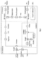
- Fig. 1 shows for better understanding a transmission / reception module according to the prior art (European Conference on Synthetic Aperture Radar 1998: Next Generation SAR, Antennas and T / R Modules, 1998, p 221 ff), of which the Invention out.
- the phase shifter and the VGA are digitally controlled by the BSU (Beam Steering Unit) via the control electronics with a resolution of 6 bits in transmit and receive mode.
- the BSU sets the amplitude and phase assignments for each of the transmit / receive modules present in the antenna.
- the RF pulse from the Tx input via the RF switch which are controlled by the BSU via the control electronics of the module, via the phase shifter and routed the VGA to the broadcast chain.
- the phase of the pulse is adjusted depending on the desired radiation direction and the gain of the VGA remains constant.
- the driver amplifier and the power amplifier work in power compression to achieve maximum efficiency.
- the coupler, detector and regulator power control loop in the transmit chain is designed to keep the output power of the HPA constant with variations in input power and temperature.
- This DC voltage is a quantity averaged over a plurality of RF pulses and represents the measure of the magnitude of the output power of the amplifier.
- the downstream P regulator controls the gate voltage of the power amplifier as a function of the output voltage of the detector circuit. This is to ensure that the power amplifier is always operated in saturation, whereby the amplifier always outputs a constant output power.
- the transmission chain is due to the energy savings only during the period of the RF pulse in operation.
- the radar echo from the receiving element of the antenna is passed via the Rx input and the circulator to the receiving branch, which amplifies the weak input signal with minimal noise.
- the first amplifier is a LNA (low noise amplifier) with low noise figure, which is protected by the non-reflective limiter from excessive input power.
- the RF switches are controlled by the BSU so that the amplified received signal is passed to the Rx output after appropriate phase and amplitude occupancy.
- the described power control loop of the transmission / reception module according to FIG. 1 keeps the output power of the power amplifier constant and thus compensates for changes in the output power due to fluctuations in the temperature and the input power of the HPA, with good efficiency at high output power becomes.
- optimizing the efficiency and especially the power consumption even at low output powers is indispensable in applications with limited power supply capacity, for example on satellites, because the power consumption of a single transceiver module adds up to the number of required modules (typical number of transmitters) / Receive modules for an antenna on a flying platform: approx. 1000) quickly to orders of magnitude, in which every unnecessarily consumed energy with high technical complexity in the service module of the satellite must be paid dearly.
- EP-B-0 473 299 a method for controlling the output power of a power amplifier is described, with which the disadvantages described can be eliminated.
- the input power according to the achievable Output power adjusted the gain is kept constant by a regulation.
- the control variable for the constant maintenance of the gain is the operating voltage of the power amplifier.
- the object of the present invention is to provide a control circuit for controlling the output power of the transmitting / receiving module, with which a stable and independent of external influences regulation is possible.
- control of the output power of the transmitting / receiving module is achieved by targeted adjustment of the input power of the transmission chain, wherein the gain of existing in the transmission chain amplifier for amplifying the RF transmission signal is always kept constant by a control. With constant gain of the amplifiers, the output power is known when the input power is adjusted with the VGA of the transmit / receive module.
- the output power of the module can be kept constant. It also allows control of this output power while meeting given requirements.
- the unnecessary consumption of generated output power by means of an attenuator as in the T / R module of FIG. 1 and too high power consumption of the amplifier of the transmission chain can be avoided.
- the power of the sidelobes can be drastically reduced by an electronically set, functional power occupancy of the antenna aperture. Furthermore, the power consumption of the entire antenna and the associated infrared radiation is greatly reduced. The lower power of the side lobes and the lower infrared radiation lead to a smaller probability of detection of the radar. The lower power consumption also relieves the power requirements on autonomous platforms (e.g., satellites).
- autonomous platforms e.g., satellites
- FIG. 2 shows the structure according to the invention modified for the transmitting / receiving module according to FIG. 1 for the transmitting branch of a transmitting / receiving module.
- the circuitry shown enables control of the output power of the transmit / receive module by selectively adjusting the input power of the transmit chain on the upstream VGA.
- the gain of the two amplifiers included in the transmission chain (driver power amplifier HPA) is controlled to a constant value.
- P in 7dBm
- P in.max 5dBm
- it makes no sense to provide excessively high input powers which are not required and, as a result of the rectification effects already mentioned, result in higher drain currents, which in turn reduce the efficiency.
- the setting of the input power of the driver amplifier is made with the VGA upstream of the transmission chain.
- the RF signal at the input and output of the driver amplifier and at the input and output of the power amplifier HPA is coupled out and the power of the RF signal is measured with correspondingly fast detectors.
- the comparison of input and output power at a comparator provides the information needed by a regulator to control the gain of the amplifiers.
- the gain is regulated by means of the gate voltage of the respective amplifier, whereby the drain-source voltage must be specified according to the set input power.
- the operating points of the amplifiers are determined by the gate and drain-source voltage.
- the gain selected will provide the amplifier with the required input power, for which in turn the associated drain-source voltage must be adjusted to keep the compression constant across all input powers.
- the required for the selected gain of the amplifier gate voltage is not specified, but adjusts itself automatically in the control loop, as soon as it is in equilibrium.
- the output power of the HPA can be varied in the range 16dB ⁇ P out ⁇ 36dBm.
- the amplifier models specified in the previous paragraph were used.
- Fig. 3 describes the control loop of the power amplifier HPA in detail.
- the corresponding control circuit of the driver amplifier is essentially identical, and is therefore not shown here.
- the subsequent amplifier is a impedance transformer which decouples the high-impedance output of the detector circuit from the subsequent loop filter TP.
- the loop filter imposes a defined dynamic behavior on the control loop and stabilizes the control. These four links form the measuring device.
- the loop filter represents a low-pass filter which is intended to limit the angular frequency response of the illustrated control loop for stability reasons at high frequencies.
- the subsequent linearizer provides a proportionality between the logarithmic output P out.dBm of the HPA and the output voltage of the detector whereby a constant control deviation X w is to be ensured with the same deviation of the amplification over all input powers as well as a constant loop gain over different gate voltages.
- the control deviation X w results after subtracting the comparison quantity u from the feedback variable r in the comparison element G v .
- an additional control deviation can be generated which simulates a disturbance of the balance between input and output power and results in a change in the gain.
- the controller G R which controls the manipulated variable y (gate voltage U G ), closes the control loop.
- a PI controller is used, which always minimizes the system deviation towards zero.
- the actuator G ST is used to decouple the regulator G R from the actuator and in addition to limit the gate voltage U G to allowable levels to protect the HPA from destruction.
- FIG. 4 shows the efficiency of the amplifier TGA9083 as a function of the output power P out and the drain-source voltage U DS .
- the output power P out was varied with the input power P in of the amplifier. It becomes clear that the efficiency is very small with small input and output powers and maximum at the highest output power.
- the exponential increase in efficiency over the logarithmically represented output power in FIG. 4 is evident from the above formula, in which input and output power increase exponentially, with the absorbed power P dc remaining virtually constant at a given drain-source voltage U DS .
- the invention provides the control of the output power of the amplifier with its input power, wherein the gain of the amplifier is to be kept constant with a control. For this, it is necessary to keep the compression of the amplifier constant with increase of the drain-source voltage U DS as soon as compression occurs with an increase in the input power.
- the exponential rise of the curves in Fig. 5 is due to the logarithmic representation of the input power.
Landscapes
- Engineering & Computer Science (AREA)
- Radar, Positioning & Navigation (AREA)
- Remote Sensing (AREA)
- Computer Networks & Wireless Communication (AREA)
- Physics & Mathematics (AREA)
- General Physics & Mathematics (AREA)
- Amplifiers (AREA)
- Variable-Direction Aerials And Aerial Arrays (AREA)
- Radar Systems Or Details Thereof (AREA)
Claims (4)
- Module d'émission/réception d'une antenne radar active commandée en phase, comprenant- un amplificateur d'amplification variable ;- une chaîne d'émission montée en aval de l'amplificateur d'amplification variable, qui comprend au moins un amplificateur pour amplifier le signal d'émission HF (Haute Fréquence), sachant que la puissance d'entrée de la chaîne d'émission peut être réglée en fonction de la puissance de sortie du module d'émission/réception à obtenir, et que le gain du ou des amplificateurs contenus dans la chaîne d'émission pour amplifier le signal d'émission HF peut être, au moyen d'un circuit de régulation, maintenu constant pour chacun des amplificateurs présents dans la chaîne d'émission, un circuit de régulation comprenant les éléments suivants :- un coupleur pour découpler le signal d'entrée d'un amplificateur dans une première boucle de régulation ;- un détecteur pour mesurer le signal d'entrée de l'amplificateur ;- un deuxième coupleur pour découpler le signal de sortie de l'amplificateur dans une deuxième boucle de régulation ;- un deuxième détecteur pour mesurer le signal de sortie de l'amplificateur ;- un comparateur pour comparer le signal d'entrée et le signal de sortie de l'amplificateur ;- un régulateur qui, à partir des informations obtenues dans le comparateur, régule le maintien du gain de l'amplificateur à une valeur constante,caractérisé en ce que le circuit de régulation contient les composants supplémentaires suivants :- des atténuateurs ayant des atténuations différentes, respectivement montés en amont des détecteurs ;- des filtres de boucle pour imprimer un comportement dynamique défini aux boucles de régulation individuelles ;- des linéarisateurs respectivement montés en aval des filtres de boucle, pour réaliser la proportionnalité entre la puissance de sortie logarithmique d'un amplificateur et la tension de sortie du détecteur.
- Module d'émission/réception selon la revendication 1, caractérisé par les composants supplémentaires suivants :- des amplificateurs de découplage respectivement montés en aval des détecteurs, pour découpler du filtre de boucle monté en aval la sortie à haute impédance du détecteur ;- un pilote de réglage, monté en aval du régulateur pour découpler le régulateur de l'entrée de grille d'un amplificateur.
- Module d'émission/réception selon la revendication 1 ou 2, caractérisé en ce que la variable réglante du circuit de régulation est la tension de grille d'un amplificateur.
- Module d'émission/réception selon l'une quelconque des revendications 1 à 3, caractérisé en ce que l'amplificateur à l'intérieur de la chaîne d'émission est un amplificateur de puissance ou un amplificateur pilote.
Applications Claiming Priority (2)
| Application Number | Priority Date | Filing Date | Title |
|---|---|---|---|
| DE10140897 | 2001-08-21 | ||
| DE2001140897 DE10140897A1 (de) | 2001-08-21 | 2001-08-21 | Verfahren zur Steuerung der Ausgangsleistung eines Sende/Empfangs-Moduls einer aktiven phasengesteuerten Radarantenne |
Publications (3)
| Publication Number | Publication Date |
|---|---|
| EP1293798A2 EP1293798A2 (fr) | 2003-03-19 |
| EP1293798A3 EP1293798A3 (fr) | 2003-08-06 |
| EP1293798B1 true EP1293798B1 (fr) | 2006-04-05 |
Family
ID=7696092
Family Applications (1)
| Application Number | Title | Priority Date | Filing Date |
|---|---|---|---|
| EP02013346A Expired - Lifetime EP1293798B1 (fr) | 2001-08-21 | 2002-06-19 | Module Emission/Reception d'une antenne radar à réseau de déphasage actif |
Country Status (2)
| Country | Link |
|---|---|
| EP (1) | EP1293798B1 (fr) |
| DE (2) | DE10140897A1 (fr) |
Cited By (1)
| Publication number | Priority date | Publication date | Assignee | Title |
|---|---|---|---|---|
| WO2009117982A2 (fr) | 2008-03-28 | 2009-10-01 | Eads Deutschland Gmbh | Procédé et dispositif pour compenser des variations d'amplification dans un circuit amplificateur |
Families Citing this family (1)
| Publication number | Priority date | Publication date | Assignee | Title |
|---|---|---|---|---|
| FR2860648B1 (fr) | 2003-10-03 | 2006-02-24 | Agence Spatiale Europeenne | Antenne de satellite de communication multi-faisceaux presentant une compensation de defaillance |
Citations (2)
| Publication number | Priority date | Publication date | Assignee | Title |
|---|---|---|---|---|
| EP0803973A1 (fr) * | 1996-04-25 | 1997-10-29 | Lucent Technologies Inc. | Amplificateur de puissance linéaire à rendement optimal utilisant le contrÔle automatique de la polarisation gate/base |
| EP0907239A1 (fr) * | 1997-10-02 | 1999-04-07 | Alcatel | Emetteur pour terminal radiotéléphonique et terminal correspondant |
Family Cites Families (2)
| Publication number | Priority date | Publication date | Assignee | Title |
|---|---|---|---|---|
| US5119042A (en) * | 1990-08-30 | 1992-06-02 | Hughes Aircraft Company | Solid state power amplifier with dynamically adjusted operating point |
| US5353031A (en) * | 1993-07-23 | 1994-10-04 | Itt Corporation | Integrated module controller |
-
2001
- 2001-08-21 DE DE2001140897 patent/DE10140897A1/de not_active Withdrawn
-
2002
- 2002-06-19 DE DE50206296T patent/DE50206296D1/de not_active Expired - Fee Related
- 2002-06-19 EP EP02013346A patent/EP1293798B1/fr not_active Expired - Lifetime
Patent Citations (2)
| Publication number | Priority date | Publication date | Assignee | Title |
|---|---|---|---|---|
| EP0803973A1 (fr) * | 1996-04-25 | 1997-10-29 | Lucent Technologies Inc. | Amplificateur de puissance linéaire à rendement optimal utilisant le contrÔle automatique de la polarisation gate/base |
| EP0907239A1 (fr) * | 1997-10-02 | 1999-04-07 | Alcatel | Emetteur pour terminal radiotéléphonique et terminal correspondant |
Cited By (4)
| Publication number | Priority date | Publication date | Assignee | Title |
|---|---|---|---|---|
| WO2009117982A2 (fr) | 2008-03-28 | 2009-10-01 | Eads Deutschland Gmbh | Procédé et dispositif pour compenser des variations d'amplification dans un circuit amplificateur |
| DE102008016154A1 (de) | 2008-03-28 | 2009-10-01 | Eads Deutschland Gmbh | Verfahren und Vorrichtung zur Kompensation von Verstärkungsänderungen bei einer Verstärkerschaltung |
| EP2346162A1 (fr) | 2008-03-28 | 2011-07-20 | EADS Deutschland GmbH | Procédé et dispositif pour compenser des variations d'amplification dans un circuit amplificateur |
| DE102008016154B4 (de) * | 2008-03-28 | 2013-08-08 | Eads Deutschland Gmbh | Verfahren zur Kompensation von Verstärkungsänderungen bei einer Verstärkerschaltung |
Also Published As
| Publication number | Publication date |
|---|---|
| DE10140897A1 (de) | 2003-03-27 |
| DE50206296D1 (de) | 2006-05-18 |
| EP1293798A3 (fr) | 2003-08-06 |
| EP1293798A2 (fr) | 2003-03-19 |
Similar Documents
| Publication | Publication Date | Title |
|---|---|---|
| DE60305505T2 (de) | Leistungssteuerungsschaltkreis für eine mobile Endgeräteanwendung | |
| DE69603220T2 (de) | Leistungssteuerungsschaltung für eine Übetragungsvorrichtung | |
| DE69719844T2 (de) | Einstellung einer aktiven phasengesteuerten Gruppenantenne durch Einstellungsbereichsmessungen der Sendeamplitude | |
| DE102009022321B4 (de) | Strategie zur Verwendung der Hüllkurveninformationen innerhalb eines Leistungssteuersystems mit geschlossener Schleife | |
| DE69434350T2 (de) | Sender und Verfahren für einen Sender zur Kompensation von veränderlicher Last ohne Isolator | |
| DE69022011T2 (de) | Verfahren zur Leistungssteuerung eines spannungsgesteuerten Leistungsverstärkers und zugehörige Schaltung. | |
| DE69223368T2 (de) | Leistungsverstärker für ein Funktelefon | |
| EP3121962B1 (fr) | Compensation d'attenuation de signal lors de la transmission de signaux d'emission d'un appareil radio mobile | |
| EP1260016B1 (fr) | Procede et circuit d'emission permettant de generer un signal d'emission | |
| DE10244167B4 (de) | Verstärkungsvorrichtung | |
| DE102010028377A1 (de) | Fahrzeugradarvorrichtung mit variabler Ausgangsleistung; gesteuert basierend auf einer Geschwindigkeit eines Fahrzeugs | |
| DE69935901T2 (de) | Mobiles tragbares Endgerät und Sendeeinrichtung mit Leistungsregelung | |
| EP0847134A1 (fr) | Circuit de linéarisation d'un amplificateur | |
| DE602004008769T2 (de) | Verfahren und Anordnung zur Einstellung der Sendeleistung eines Mobilübertragungsgerätes | |
| EP1293798B1 (fr) | Module Emission/Reception d'une antenne radar à réseau de déphasage actif | |
| DE3742270C1 (en) | Control stage for a radio-frequency power amplifier | |
| WO2003005564A2 (fr) | Procede de regulation de l'amplification d'un signal haute frequence | |
| DE60301338T2 (de) | Verstärkerschaltungen und ihre verwendung in hochfrequenzsendern | |
| DE102005008372A1 (de) | Steuerbarer Verstärker und dessen Verwendung | |
| EP1203447B1 (fr) | Procede et dispositif pour faire fonctionner un amplificateur de puissance hf | |
| DE102009029422B4 (de) | Sender mit Hybrid-Leistungsregelung | |
| EP1999845B1 (fr) | Dispositif et procédé de réglage d'amplification dépendant des paramètres de fonctionnement dans des dispositifs radio | |
| EP3311596A1 (fr) | Dispositif de compensation, en particulier dispositif de compensation indépendant d'un jeu de puces pour une communication c2c | |
| DE19606799A1 (de) | Anordnung zur Regelung der Ausgangsamplitude eines Hochfrequenz-Leistungsverstärkers | |
| DE102006038410B3 (de) | Vorrichtung und Verfahren zur Regelung der Ausgangsleistung einer Verstärkerstufe |
Legal Events
| Date | Code | Title | Description |
|---|---|---|---|
| PUAI | Public reference made under article 153(3) epc to a published international application that has entered the european phase |
Free format text: ORIGINAL CODE: 0009012 |
|
| AK | Designated contracting states |
Kind code of ref document: A2 Designated state(s): AT BE CH CY DE DK ES FI FR GB GR IE IT LI LU MC NL PT SE TR Designated state(s): AT BE CH CY DE DK ES FI FR GB GR IE IT LI LU MC NL PT SE TR |
|
| AX | Request for extension of the european patent |
Extension state: AL LT LV MK RO SI |
|
| PUAL | Search report despatched |
Free format text: ORIGINAL CODE: 0009013 |
|
| AK | Designated contracting states |
Designated state(s): AT BE CH CY DE DK ES FI FR GB GR IE IT LI LU MC NL PT SE TR |
|
| AX | Request for extension of the european patent |
Extension state: AL LT LV MK RO SI |
|
| 17P | Request for examination filed |
Effective date: 20030911 |
|
| 17Q | First examination report despatched |
Effective date: 20040303 |
|
| AKX | Designation fees paid |
Designated state(s): DE FR GB IT NL |
|
| RTI1 | Title (correction) |
Free format text: TRANSMIT/RECEIVE MODULE OF AN ACTIVE PHASED ARRAY RADAR ANTENNA |
|
| GRAP | Despatch of communication of intention to grant a patent |
Free format text: ORIGINAL CODE: EPIDOSNIGR1 |
|
| GRAS | Grant fee paid |
Free format text: ORIGINAL CODE: EPIDOSNIGR3 |
|
| GRAA | (expected) grant |
Free format text: ORIGINAL CODE: 0009210 |
|
| AK | Designated contracting states |
Kind code of ref document: B1 Designated state(s): DE FR GB IT NL |
|
| REG | Reference to a national code |
Ref country code: GB Ref legal event code: FG4D Free format text: NOT ENGLISH |
|
| REF | Corresponds to: |
Ref document number: 50206296 Country of ref document: DE Date of ref document: 20060518 Kind code of ref document: P |
|
| PGFP | Annual fee paid to national office [announced via postgrant information from national office to epo] |
Ref country code: NL Payment date: 20060614 Year of fee payment: 5 |
|
| PGFP | Annual fee paid to national office [announced via postgrant information from national office to epo] |
Ref country code: GB Payment date: 20060615 Year of fee payment: 5 |
|
| PGFP | Annual fee paid to national office [announced via postgrant information from national office to epo] |
Ref country code: DE Payment date: 20060616 Year of fee payment: 5 |
|
| PGFP | Annual fee paid to national office [announced via postgrant information from national office to epo] |
Ref country code: FR Payment date: 20060619 Year of fee payment: 5 |
|
| PGFP | Annual fee paid to national office [announced via postgrant information from national office to epo] |
Ref country code: IT Payment date: 20060630 Year of fee payment: 5 |
|
| GBT | Gb: translation of ep patent filed (gb section 77(6)(a)/1977) |
Effective date: 20060612 |
|
| ET | Fr: translation filed | ||
| PLBE | No opposition filed within time limit |
Free format text: ORIGINAL CODE: 0009261 |
|
| STAA | Information on the status of an ep patent application or granted ep patent |
Free format text: STATUS: NO OPPOSITION FILED WITHIN TIME LIMIT |
|
| 26N | No opposition filed |
Effective date: 20070108 |
|
| GBPC | Gb: european patent ceased through non-payment of renewal fee |
Effective date: 20070619 |
|
| NLV4 | Nl: lapsed or anulled due to non-payment of the annual fee |
Effective date: 20080101 |
|
| REG | Reference to a national code |
Ref country code: FR Ref legal event code: ST Effective date: 20080229 |
|
| PG25 | Lapsed in a contracting state [announced via postgrant information from national office to epo] |
Ref country code: NL Free format text: LAPSE BECAUSE OF NON-PAYMENT OF DUE FEES Effective date: 20080101 Ref country code: DE Free format text: LAPSE BECAUSE OF NON-PAYMENT OF DUE FEES Effective date: 20080101 |
|
| PG25 | Lapsed in a contracting state [announced via postgrant information from national office to epo] |
Ref country code: GB Free format text: LAPSE BECAUSE OF NON-PAYMENT OF DUE FEES Effective date: 20070619 |
|
| PG25 | Lapsed in a contracting state [announced via postgrant information from national office to epo] |
Ref country code: FR Free format text: LAPSE BECAUSE OF NON-PAYMENT OF DUE FEES Effective date: 20070702 |
|
| PG25 | Lapsed in a contracting state [announced via postgrant information from national office to epo] |
Ref country code: IT Free format text: LAPSE BECAUSE OF NON-PAYMENT OF DUE FEES Effective date: 20070619 |