EP1296320A2 - Méthode d'enregistrement/reproduction de données à haute densité, utilisant l'émission d'électrons et des milieux à changement de phase et système d'enregistrement de données l'adoptant et milieux pour le système - Google Patents
Méthode d'enregistrement/reproduction de données à haute densité, utilisant l'émission d'électrons et des milieux à changement de phase et système d'enregistrement de données l'adoptant et milieux pour le système Download PDFInfo
- Publication number
- EP1296320A2 EP1296320A2 EP02255382A EP02255382A EP1296320A2 EP 1296320 A2 EP1296320 A2 EP 1296320A2 EP 02255382 A EP02255382 A EP 02255382A EP 02255382 A EP02255382 A EP 02255382A EP 1296320 A2 EP1296320 A2 EP 1296320A2
- Authority
- EP
- European Patent Office
- Prior art keywords
- data recording
- electrons
- recording layer
- media
- electron
- Prior art date
- Legal status (The legal status is an assumption and is not a legal conclusion. Google has not performed a legal analysis and makes no representation as to the accuracy of the status listed.)
- Withdrawn
Links
Images


Classifications
-
- G—PHYSICS
- G11—INFORMATION STORAGE
- G11B—INFORMATION STORAGE BASED ON RELATIVE MOVEMENT BETWEEN RECORD CARRIER AND TRANSDUCER
- G11B9/00—Recording or reproducing using a method not covered by one of the main groups G11B3/00 - G11B7/00; Record carriers therefor
- G11B9/10—Recording or reproducing using a method not covered by one of the main groups G11B3/00 - G11B7/00; Record carriers therefor using electron beam; Record carriers therefor
-
- B—PERFORMING OPERATIONS; TRANSPORTING
- B82—NANOTECHNOLOGY
- B82Y—SPECIFIC USES OR APPLICATIONS OF NANOSTRUCTURES; MEASUREMENT OR ANALYSIS OF NANOSTRUCTURES; MANUFACTURE OR TREATMENT OF NANOSTRUCTURES
- B82Y10/00—Nanotechnology for information processing, storage or transmission, e.g. quantum computing or single electron logic
-
- G—PHYSICS
- G11—INFORMATION STORAGE
- G11B—INFORMATION STORAGE BASED ON RELATIVE MOVEMENT BETWEEN RECORD CARRIER AND TRANSDUCER
- G11B9/00—Recording or reproducing using a method not covered by one of the main groups G11B3/00 - G11B7/00; Record carriers therefor
- G11B9/12—Recording or reproducing using a method not covered by one of the main groups G11B3/00 - G11B7/00; Record carriers therefor using near-field interactions; Record carriers therefor
- G11B9/14—Recording or reproducing using a method not covered by one of the main groups G11B3/00 - G11B7/00; Record carriers therefor using near-field interactions; Record carriers therefor using microscopic probe means, i.e. recording or reproducing by means directly associated with the tip of a microscopic electrical probe as used in Scanning Tunneling Microscopy [STM] or Atomic Force Microscopy [AFM] for inducing physical or electrical perturbations in a recording medium; Record carriers or media specially adapted for such transducing of information
-
- G—PHYSICS
- G11—INFORMATION STORAGE
- G11B—INFORMATION STORAGE BASED ON RELATIVE MOVEMENT BETWEEN RECORD CARRIER AND TRANSDUCER
- G11B9/00—Recording or reproducing using a method not covered by one of the main groups G11B3/00 - G11B7/00; Record carriers therefor
- G11B9/12—Recording or reproducing using a method not covered by one of the main groups G11B3/00 - G11B7/00; Record carriers therefor using near-field interactions; Record carriers therefor
- G11B9/14—Recording or reproducing using a method not covered by one of the main groups G11B3/00 - G11B7/00; Record carriers therefor using near-field interactions; Record carriers therefor using microscopic probe means, i.e. recording or reproducing by means directly associated with the tip of a microscopic electrical probe as used in Scanning Tunneling Microscopy [STM] or Atomic Force Microscopy [AFM] for inducing physical or electrical perturbations in a recording medium; Record carriers or media specially adapted for such transducing of information
- G11B9/1409—Heads
-
- G—PHYSICS
- G11—INFORMATION STORAGE
- G11B—INFORMATION STORAGE BASED ON RELATIVE MOVEMENT BETWEEN RECORD CARRIER AND TRANSDUCER
- G11B9/00—Recording or reproducing using a method not covered by one of the main groups G11B3/00 - G11B7/00; Record carriers therefor
- G11B9/12—Recording or reproducing using a method not covered by one of the main groups G11B3/00 - G11B7/00; Record carriers therefor using near-field interactions; Record carriers therefor
- G11B9/14—Recording or reproducing using a method not covered by one of the main groups G11B3/00 - G11B7/00; Record carriers therefor using near-field interactions; Record carriers therefor using microscopic probe means, i.e. recording or reproducing by means directly associated with the tip of a microscopic electrical probe as used in Scanning Tunneling Microscopy [STM] or Atomic Force Microscopy [AFM] for inducing physical or electrical perturbations in a recording medium; Record carriers or media specially adapted for such transducing of information
- G11B9/1418—Disposition or mounting of heads or record carriers
-
- G—PHYSICS
- G11—INFORMATION STORAGE
- G11B—INFORMATION STORAGE BASED ON RELATIVE MOVEMENT BETWEEN RECORD CARRIER AND TRANSDUCER
- G11B9/00—Recording or reproducing using a method not covered by one of the main groups G11B3/00 - G11B7/00; Record carriers therefor
- G11B9/12—Recording or reproducing using a method not covered by one of the main groups G11B3/00 - G11B7/00; Record carriers therefor using near-field interactions; Record carriers therefor
- G11B9/14—Recording or reproducing using a method not covered by one of the main groups G11B3/00 - G11B7/00; Record carriers therefor using near-field interactions; Record carriers therefor using microscopic probe means, i.e. recording or reproducing by means directly associated with the tip of a microscopic electrical probe as used in Scanning Tunneling Microscopy [STM] or Atomic Force Microscopy [AFM] for inducing physical or electrical perturbations in a recording medium; Record carriers or media specially adapted for such transducing of information
- G11B9/1463—Record carriers for recording or reproduction involving the use of microscopic probe means
-
- G—PHYSICS
- G11—INFORMATION STORAGE
- G11B—INFORMATION STORAGE BASED ON RELATIVE MOVEMENT BETWEEN RECORD CARRIER AND TRANSDUCER
- G11B11/00—Recording on or reproducing from the same record carrier wherein for these two operations the methods are covered by different main groups of groups G11B3/00 - G11B7/00 or by different subgroups of group G11B9/00; Record carriers therefor
- G11B11/10—Recording on or reproducing from the same record carrier wherein for these two operations the methods are covered by different main groups of groups G11B3/00 - G11B7/00 or by different subgroups of group G11B9/00; Record carriers therefor using recording by magnetic means or other means for magnetisation or demagnetisation of a record carrier, e.g. light induced spin magnetisation; Demagnetisation by thermal or stress means in the presence or not of an orienting magnetic field
- G11B11/115—Recording on or reproducing from the same record carrier wherein for these two operations the methods are covered by different main groups of groups G11B3/00 - G11B7/00 or by different subgroups of group G11B9/00; Record carriers therefor using recording by magnetic means or other means for magnetisation or demagnetisation of a record carrier, e.g. light induced spin magnetisation; Demagnetisation by thermal or stress means in the presence or not of an orienting magnetic field using a beam,e.g. of electrons or X-rays other than a beam of light for reproducing
Definitions
- the present invention relates to a data recording/reproduction method through scanning an electron beam into a phase change media, a data recording system adopting the same, and media for the system.
- Compact discs (CDs) and digital versatile discs (DVDs) in which laser is used for recording and reproducing data have limited data recording density due to limitations on laser wavelength.
- a data storage system using a vertical magnetic recording method having a comparatively high recording density also has limited recording density due to the size of a probe for approaching media and recording or reproducing data.
- a scanning electron microscope (SEM) method utilizing an electron beam, and a transmission electron microscope (TEM) method can achieve very high recording density of data.
- SEM scanning electron microscope
- TEM transmission electron microscope
- a data recording method comprising the steps of: preparing media having a data recording layer in which a phase change is generated through electron absorption; generating electrons using an electron generating source according to data for recording at a position separated from the data recording layer by a predetermined interval; forming a magnetic field on the path of the electrons, and cyclotron moving the electrons; and transmitting the cyclotron moved electrons onto the data recording layer and performing data recording through local melting and cooling due to the absorption of the electrons by the data recording layer.
- the interval between the electron generating source and the data recording layer is controlled such that the electrons are rotated once or an integer multiple of times during cyclotron movement, after the electrons have been emitted by the electron generating source.
- an electric field emitting means including a micro-tip for emitting electrons and a gate electrode interposed between the micro-tip and the data recording layer, is adopted as the electron generating source.
- the magnetic field on the path of the electrons is perpendicular to the data recording layer, and the magnetic filed is formed by a direct current (DC) magnetic field forming means positioned at both sides of the electron generating source and the media.
- DC direct current
- a data recording system comprising: media having a data recording layer in which a phase change is generated through electron absorption; an electron generating source installed at a position separated from the data recording layer by a predetermined interval, for emitting electrons according to data for recording on the data recording layer; and a magnetic field generating source, for forming a magnetic field for cyclotron movement of the electrons, on the path of the electrons between the electron generating source and the media.
- the interval between the electron generating source and the data recording layer is controlled such that the electrons are rotated once or an integer multiple of times during cyclotron movement, after the electrons have been emitted by the electron generating source.
- the electron generating source includes a micro-tip for emitting electrons using an electric field, and a gate electrode for controlling electron emission from the micro-tip, and the interval between the gate electrode and the micro-tip and/or the interval between the gate electrode and the media can be controlled.
- the magnetic field generating source forms a magnetic field perpendicular to the data recording layer.
- the system includes a direct current (DC) magnetic field forming means formed of a permanent magnet or an electromagnet, which is positioned at both sides of the electron generating source and the media.
- DC direct current
- media for a data recording system comprising: a data recording layer in which a phase change is generated through electron absorption, and a conductive substrate for supporting the data recording layer.
- the data recording layer includes a phase change material layer formed on the entire surface of the substrate, and an insulation layer having channels formed at a predetermined spacing, on the phase change material layer.
- the data recording method and the data recording system according to the invention store and erase data by remotely scanning an electron beam into media for high density data storage and data decryption, detect scattering of the electron beam from media by scanning the electron beam into stored data, or detect current flowing through a recording portion, thereby decrypting data.
- the invention thus provides a data recording/reproduction/tracking method having a high recording density and allowing miniaturization, a data recording system adopting the same, and media for the system.
- an electron generating source 10 including a gate electrode 12 and a micro-tip 11 is positioned above media 20 including a data recording layer 22 having a data recording region formed of a phase change material such as GeTeSb, and a substrate 21 for supporting the data recording layer 22.
- the micro-tip 11 is held at the end of a conductive cantilever 11a, and a vertical magnetic field B is formed by a magnetic field generating source 30.
- an upper magnetic field generating source 31 and a lower magnetic field generating source 32 constituting the magnetic field generating source 30 are respectively positioned above the electron generating source 10 and below the media 20.
- the micro-tip 11 and the gate electrode 12 below the micro-tip 11 basically adopt an electric field emission structure.
- An emitter for emitting electrons through an electric field that is, the gate electrode 12 below the micro-tip 11, has a gate hole 12a through which electrons pass.
- Electron detectors 60 and 60a for detecting scattering electrons or secondary electrons generated through electron collision from the data recording layer 22 are positioned below the gate electrode 12.
- the gate electrode 12 controls electron emission caused by the micro-tip 11, and simultaneously converges a beam generated by emitted electrons around the gate hole 12a, essentially near the lower portion of the gate hole 12a.
- the micro-tip 11 is biased to a negative voltage by a driving circuit 40, and a predetermined positive voltage is applied to the gate electrode 12.
- the substrate 21 of the media 20 is a kind of collector, and a positive substrate voltage, higher than the gate voltage, is applied to the substrate 21.
- the gate voltage and the substrate voltage are properly varied by the driving circuit 40, thereby controlling electron emission from the micro-tip 11 and electron collision with the data recording layer 22 of the media 20.
- the voltage applying structure is adopted from a conventional field emission structure having three poles, and thus will be not further described.
- the upper and lower magnetic field generating sources 31 and 32 of the magnetic field generating source 30 adopts a permanent magnet or an electromagnet, to form magnetic flux passing perpendicularly through the media 20. Due to the magnetic flux and an electric field between the gate electrode 12 and the media 20, cyclotron movement of the electron beam 50 between the gate electrode 12 and the media 20 is generated. That is, electrons which passed the gate electrode 12 after being emitted from the micro-tip 11 are rotated by the magnetic field and the electric field parallel with the magnetic field and go into the data recording layer 22.
- the data recording layer 22 is locally melted and cooled.
- a local amorphous portion 22a is generated in the data recording layer 22.
- the amorphous portion, that is, a data dot, 22a is generated in a minor hole or groove of the data recording layer 22 filled with a phase change material to be later described according to an embodiment of the present invention.
- the present invention must give electrons a high kinetic energy through cyclotron movement, causing the electrons to collide with the data recording layer 22 to form a data dot of an amorphous/crystalline portion, and recording data.
- the size of a data portion caused by electron collision is inversely proportional to data recording density. That is, if the data portion is large, the data recording density is low, and in the reverse case, the data recording density is high.
- the size of the data portion can be a quantum dot of an atomic size, what is called, by properly adjusting the distance between the gate electrode 12 and the data recording layer 22 according to a preferred embodiment of the present invention.
- the distance between the gate electrode 12 and the data recording layer 22 is set such that rotating electrons emitted from the micro-tip 11 and proceeding in the form of whirlwind reach the data recording layer 22 after one rotation, but may also be set as a multiple of that distance if the occasion demands.
- FIG. 3 is a schematic cross-sectional view of media according to an embodiment of the present invention.
- the media 20 in the present embodiment includes a phase change material layer 22 formed on the conductive substrate 21, and a dielectric material layer 22a having a strip shape formed on the phase change material layer 22 at predetermined intervals.
- a portion not covered by the dielectric material layer 22a corresponds to a groove 22b in which data is recorded by electrons e - .
- the electrons emitted from the micro-tip 11 cyclotron are moved by an electric field between the gate electrode 12 and the substrate 21 and a magnetic field parallel to the electric field, and converge on a dot with a one-to-one correspondence to the position where the electrons were generated regardless of scattering of the beam, if the magnetic field is controlled such that the electrons rotate once within the distance between the micro-tip 11 and the substrate 21.
- the kinetic energy of the electrons causes them to penetrate the data recording layer 22 formed of a phase change material and generate heat, changing the phase of a portion where the electrons are absorbed.
- the kinetic energy of the electrons is controlled by the voltage between the gate electrode 12 and the substrate 21.
- the size of the magnetic field through path of the electrons is determined by the voltage and the distance between the surface of the gate electrode 12 and the surface of the data recording layer 22.
- the distance between the gate electrode 12 and the data recording layer 22 is constantly maintained, and recording data on the data recording layer 22 is controlled by variation in the electric field and the magnetic field.
- the position of the micro-tip 11 relative to the gate electrode 12 below the micro-tip 11 is fixed, and the data recording layer 22 may be moved.
- the structure may be adopted in a conventional vertical magnetic recording method or a conventional magnetic recording method.
- FIG. 4 illustrates the principle in which a portion is formed through amorphism during writing in a state where a writing magnetic field Bw is applied
- FIG. 5 illustrates crystallization during writing (specifically, during erasing) in a state where an erase magnetic file Be is applied.
- the phase of a phase change material constituting the data recording layer 22 is determined by the kinetic energy of incident electrons.
- the kinetic energy of the electrons reaching the surface of the data recording layer 22 is eVw.
- e is 1.6 x 10 -19 coul.
- the recording voltage Vw is determined such that the phase change material is sufficiently melted by the energy of eVw. The melted portion instantly cools, and thus is left in an amorphous state. This is a process of recording data through amorphism.
- an erase voltage Ve lower than the recording voltage Vw is applied, and the electrons colliding with the surface of the data recording layer 22 are absorbed to generate sufficient heat to crystallize the data recording layer 22.
- FIG. 6 illustrates the principle in which an amorphous portion is read when a vertical reading magnetic field Br is applied
- FIG. 7 illustrates the principle in which a crystalline portion is read.
- the lowest reading voltage Vr is applied.
- the reading voltage Vr has a sufficiently small potential, so that the kinetic energy of eVr causes no phase change on the data recording layer 22.
- the electrons colliding with the substrate 21 of the data recording layer 22 with energy of eVR are scattered and absorbed, generating secondary electrons.
- the degree of scattering of the electrons varies depending on the phase of the portion where the electrons strike. That is, as shown in FIG. 6, the electrons scatter very briskly at the amorphous portion, and as shown in FIG. 7, scatter less at the crystalline portion.
- the phase at the portion where the electrons strike may be detected by the above electron detectors installed near the scattering region of the electrons, according to the scattering of the electrons.
- FIG. 8 illustrates a reading method shown in FIGS. 6 and 7 and the principle of reading data according to another variation in current.
- a detector for detecting current such as an ammeter 70 or a sensor, is provided on an electrical path between the conductive substrate 21 of the medial 20 and the gate electrode 12.
- a detector for detecting current such as an ammeter 70 or a sensor
- the current between the media 20 and the gate electrode 12 varies according to the crystalline and amorphous portions.
- the magnitude and variation of the current are small, and thus, preferably, the ammeter 70 has a separate current amplifier.
- the data recording region is limited by a dielectric layer or an electrical insulation layer, and thereby a portion where actual data will be recorded is either formed in a groove of a restricted size, or exposed by an insulation layer, so as to allow the portion where the electron beam strikes to be precisely tracked. This is referred to as pre-formatting.
- FIG. 9A through 9E A process of manufacturing the media shown in FIG. 3 according to the embodiment of the present invention will be described with reference to FIGS. 9A through 9E.
- the phase change material layer 22 is formed on the prepared conductive substrate 21.
- an insulation layer 22a is formed on the phase change material layer 22, and a polymer layer 80 is formed on the insulation layer 22a.
- grooves for recording data are formed on the insulation layer 22a by stamping with a stamp 90 having protrusions formed at a predetermined spacing.
- the thin portion of the polymer layer 80 is first etched through etching, and thereby the insulation layer 22a under the polymer layer 80 is etched, and the phase change material 22 is exposed at the bottom of the groove.
- the polymer layer 80 remaining on the insulation layer 22a is removed.
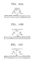
- FIGS. 10A through 10C illustrate the types of tracking errors according to the position of impact of the electron beam in the data recording system utilizing the media shown in FIG. 3 as recording media according to the present invention.
- FIG. 10A illustrates a state where the electron beam precisely strikes the center of the groove. Scattering of the electrons or secondary electrons occurs uniformly in all directions, and thus equal amounts within a predetermined range are detected by the electron detectors above the scattering region of the electrons. In such a case, there are no tracking errors, and thus tracking correction of the electron generating source is unnecessary.
- FIGS. 10B and 10C illustrate a state where the electron beam strikes one side of the bottom of the groove or the insulation layer above the groove.
- the electrons or secondary electrons are scattered briskly in one direction.
- more electrons are detected by one of the two electron detectors above the scattering region of the electrons.
- there are tracking errors and thus a tracking correction must be made to the electron generating source to return to the state of FIG. 10A after trials and errors.
- the micro-tip does not contact the data recording layer while the electron beam collides with the data recording layer, and thus no damage is caused by waste of the micro-tip, as with a conventional AFM method, and data recording and reproduction is very fast.
- the electron beam is converged onto the data recording layer through cyclotron movement, and thus the region where the electron beam reaches can be minimized by properly adjusting the distance, to maximize the data recording density.
Landscapes
- Engineering & Computer Science (AREA)
- Physics & Mathematics (AREA)
- Chemical & Material Sciences (AREA)
- Nanotechnology (AREA)
- Plasma & Fusion (AREA)
- Mathematical Physics (AREA)
- Theoretical Computer Science (AREA)
- Crystallography & Structural Chemistry (AREA)
- Optical Recording Or Reproduction (AREA)
- Magnetic Record Carriers (AREA)
Applications Claiming Priority (2)
| Application Number | Priority Date | Filing Date | Title |
|---|---|---|---|
| KR10-2001-0058854A KR100429843B1 (ko) | 2001-09-22 | 2001-09-22 | 전자 방출 및 상변화물질을 이용한 고밀도정보기록/재생방법 및 이를 응용한 정보저장장치 및 이에사용되는 미디어 |
| KR2001058854 | 2001-09-22 |
Publications (2)
| Publication Number | Publication Date |
|---|---|
| EP1296320A2 true EP1296320A2 (fr) | 2003-03-26 |
| EP1296320A3 EP1296320A3 (fr) | 2008-02-27 |
Family
ID=36811288
Family Applications (1)
| Application Number | Title | Priority Date | Filing Date |
|---|---|---|---|
| EP02255382A Withdrawn EP1296320A3 (fr) | 2001-09-22 | 2002-08-01 | Méthode d'enregistrement/reproduction de données à haute densité, utilisant l'émission d'électrons et des milieux à changement de phase et système d'enregistrement de données l'adoptant et milieux pour le système |
Country Status (5)
| Country | Link |
|---|---|
| US (1) | US7355951B2 (fr) |
| EP (1) | EP1296320A3 (fr) |
| JP (1) | JP4104943B2 (fr) |
| KR (1) | KR100429843B1 (fr) |
| CN (2) | CN1237530C (fr) |
Cited By (1)
| Publication number | Priority date | Publication date | Assignee | Title |
|---|---|---|---|---|
| DE102008038803A1 (de) * | 2008-08-13 | 2010-02-18 | Fraunhofer-Gesellschaft zur Förderung der angewandten Forschung e.V. | Verfahren und Vorrichtung zur Langzeitarchivierung von Daten |
Families Citing this family (9)
| Publication number | Priority date | Publication date | Assignee | Title |
|---|---|---|---|---|
| US20050232061A1 (en) * | 2004-04-16 | 2005-10-20 | Rust Thomas F | Systems for writing and reading highly resolved domains for high density data storage |
| JP4732211B2 (ja) * | 2006-03-28 | 2011-07-27 | 株式会社日立製作所 | 磁気記録装置 |
| US20070121477A1 (en) * | 2006-06-15 | 2007-05-31 | Nanochip, Inc. | Cantilever with control of vertical and lateral position of contact probe tip |
| US20070290282A1 (en) * | 2006-06-15 | 2007-12-20 | Nanochip, Inc. | Bonded chip assembly with a micro-mover for microelectromechanical systems |
| US20070291623A1 (en) * | 2006-06-15 | 2007-12-20 | Nanochip, Inc. | Cantilever with control of vertical and lateral position of contact probe tip |
| US20080074792A1 (en) * | 2006-09-21 | 2008-03-27 | Nanochip, Inc. | Control scheme for a memory device |
| US20080074984A1 (en) * | 2006-09-21 | 2008-03-27 | Nanochip, Inc. | Architecture for a Memory Device |
| WO2012176948A1 (fr) * | 2011-06-24 | 2012-12-27 | 한국표준과학연구원 | Appareil de mesure de fusion |
| CN111508535B (zh) | 2020-03-13 | 2021-08-13 | 华为技术有限公司 | 一种数据写入读取方法、装置及系统 |
Family Cites Families (32)
| Publication number | Priority date | Publication date | Assignee | Title |
|---|---|---|---|---|
| US2952503A (en) * | 1955-06-13 | 1960-09-13 | Trionics Corp | Method and apparatus for magnetic recording and reproducing |
| DE3512715A1 (de) * | 1984-04-09 | 1985-10-24 | Victor Company Of Japan, Ltd., Yokohama, Kanagawa | Verfahren und vorrichtung zur aufzeichnung und wiedergabe von signalen mittels aufzeichnungsplatten |
| EP0243976B1 (fr) * | 1986-05-02 | 1996-09-04 | Hitachi, Ltd. | Méthode pour l'enregistrement, la reproduction et l'effaçement d'informations et film mince pour l'enregistrement d'informations |
| JPS6318541A (ja) * | 1986-07-11 | 1988-01-26 | Hitachi Ltd | 電子線記録再生方法及びその装置 |
| US4760567A (en) * | 1986-08-11 | 1988-07-26 | Electron Beam Memories | Electron beam memory system with ultra-compact, high current density electron gun |
| US5270990A (en) * | 1986-08-15 | 1993-12-14 | Canon Kabushiki Kaisha | Tracking error signal detecting apparatus using an electron beam and apparatus for effecting recording/reproduction of information by the utilization of a plurality of electron beams |
| US5006395A (en) * | 1987-05-12 | 1991-04-09 | Matsushita Electric Industrial Co., Ltd. | Iron carbide thin film magnetic recording medium |
| JPS63281246A (ja) | 1987-05-13 | 1988-11-17 | Hitachi Ltd | 電子線記録再生装置 |
| JP2553100B2 (ja) * | 1987-09-02 | 1996-11-13 | 株式会社東芝 | 情報記録媒体の情報操作方法 |
| US5270995A (en) * | 1989-01-13 | 1993-12-14 | Sharp Kabushiki Kaisha | Method for recording and reproducing information by varying a work function of a recording medium and device for the same |
| JP2773350B2 (ja) | 1990-02-01 | 1998-07-09 | 日本電気株式会社 | 電子線記憶方法および電子線記憶素子とその製造方法 |
| US5350618A (en) * | 1991-03-01 | 1994-09-27 | Teijin Seiki Co., Ltd. | Magnetic medium comprising a substrate having pits and grooves of specific shapes and depths |
| US5368986A (en) * | 1991-05-02 | 1994-11-29 | Hitachi, Ltd. | Information recording media, manufacturing method for the same, and information recording method |
| JPH05159735A (ja) | 1991-12-03 | 1993-06-25 | Pioneer Electron Corp | 電子ビーム投射装置 |
| US5395738A (en) * | 1992-12-29 | 1995-03-07 | Brandes; George R. | Electron lithography using a photocathode |
| JPH06251435A (ja) * | 1993-03-01 | 1994-09-09 | Canon Inc | 記録再生装置 |
| EP0619576B1 (fr) * | 1993-04-05 | 1999-12-15 | Canon Kabushiki Kaisha | Procédé de fabrication d'un support d'enregistrement optique |
| KR950024146A (ko) * | 1994-01-31 | 1995-08-21 | 모리시타 요이찌 | 정보기록재생장치 및 정보기록재생방법 |
| KR100257705B1 (ko) * | 1996-03-19 | 2000-06-01 | 김덕중 | 실리콘 팁 필드 에미터의 제조방법 |
| JP3526374B2 (ja) * | 1996-07-26 | 2004-05-10 | 株式会社東芝 | 相変化光記録媒体および光記録方法 |
| JPH10241211A (ja) * | 1997-02-27 | 1998-09-11 | Tdk Corp | 光記録媒体の製造方法 |
| JPH11144319A (ja) * | 1997-11-06 | 1999-05-28 | Toshiba Corp | 光学的情報記録媒体及び記録再生方法 |
| US5962859A (en) * | 1998-01-09 | 1999-10-05 | International Business Machines Corporation | Multiple variable shaped electron beam system with lithographic structure |
| US5981962A (en) * | 1998-01-09 | 1999-11-09 | International Business Machines Corporation | Distributed direct write lithography system using multiple variable shaped electron beams |
| US6175122B1 (en) * | 1998-01-09 | 2001-01-16 | International Business Machines Corporation | Method for writing a pattern using multiple variable shaped electron beams |
| KR100549445B1 (ko) * | 1999-07-30 | 2006-02-07 | 한국전자통신연구원 | 고집적 고속 정보기록판독장치 |
| US6741524B2 (en) * | 1999-12-28 | 2004-05-25 | Kabushiki Kaisha Toshiba | Thermally-assisted magnetic recording and reproducing device having an electron beam thermal source |
| JP2002025146A (ja) * | 2000-07-11 | 2002-01-25 | Ricoh Co Ltd | 記録媒体 |
| US6473388B1 (en) * | 2000-08-31 | 2002-10-29 | Hewlett Packard Company | Ultra-high density information storage device based on modulated cathodoconductivity |
| US6735163B2 (en) * | 2001-03-02 | 2004-05-11 | Hewlett-Packard Development Company, L.P. | Ultra-high density storage device with resonant scanning micromover |
| US6607415B2 (en) * | 2001-06-12 | 2003-08-19 | Hewlett-Packard Development Company, L.P. | Method for fabricating tiny field emitter tips |
| US6700853B2 (en) * | 2001-07-20 | 2004-03-02 | Hewlett-Packard Development Company, Lp. | Data storage devices with wafer alignment compensation |
-
2001
- 2001-09-22 KR KR10-2001-0058854A patent/KR100429843B1/ko not_active Expired - Fee Related
-
2002
- 2002-08-01 EP EP02255382A patent/EP1296320A3/fr not_active Withdrawn
- 2002-08-13 CN CNB021297541A patent/CN1237530C/zh not_active Expired - Fee Related
- 2002-08-13 CN CNA2005101247479A patent/CN1801361A/zh active Pending
- 2002-09-17 JP JP2002270422A patent/JP4104943B2/ja not_active Expired - Fee Related
- 2002-09-23 US US10/252,085 patent/US7355951B2/en not_active Expired - Fee Related
Cited By (1)
| Publication number | Priority date | Publication date | Assignee | Title |
|---|---|---|---|---|
| DE102008038803A1 (de) * | 2008-08-13 | 2010-02-18 | Fraunhofer-Gesellschaft zur Förderung der angewandten Forschung e.V. | Verfahren und Vorrichtung zur Langzeitarchivierung von Daten |
Also Published As
| Publication number | Publication date |
|---|---|
| CN1409311A (zh) | 2003-04-09 |
| CN1237530C (zh) | 2006-01-18 |
| JP2003141786A (ja) | 2003-05-16 |
| KR100429843B1 (ko) | 2004-05-03 |
| KR20030025687A (ko) | 2003-03-29 |
| JP4104943B2 (ja) | 2008-06-18 |
| US20030058749A1 (en) | 2003-03-27 |
| EP1296320A3 (fr) | 2008-02-27 |
| US7355951B2 (en) | 2008-04-08 |
| CN1801361A (zh) | 2006-07-12 |
Similar Documents
| Publication | Publication Date | Title |
|---|---|---|
| US7355951B2 (en) | High density data recording/reproduction method utilizing electron emission and phase change media, and data recording system adopting the same, and media for the system | |
| EP1233412A2 (fr) | Dispositif de stockage de données | |
| JP3801468B2 (ja) | 変調された陰極導電率に基づく超高密度情報記憶装置 | |
| US7068582B2 (en) | Read head for ultra-high-density information storage media and method for making the same | |
| US7057997B2 (en) | Class of electron beam based data storage devices and methods of use thereof | |
| US20030053399A1 (en) | High-density information storage apparatus using electron emission and methods of writing, reading and erasing information using the same | |
| JP4629314B2 (ja) | 原子分解能記憶デバイス | |
| US6400655B1 (en) | Near field optical information system with seperated recording and reproducing inclined head | |
| JPS62245530A (ja) | 微細ビ−ム利用超高密度記録方式 | |
| Katsumura et al. | High-density groove mastering using an electron beam recorder and plasma etching process | |
| US6930971B2 (en) | Ultra-high density storage device with electron beam steering | |
| KR930007179B1 (ko) | 정보기록과 재생방법 및 그의 장치 | |
| US6791931B2 (en) | Accelerometer using field emitter technology | |
| Ichimura et al. | Near-field optical recording on a pre-grooved phase-change disk in the blue-violet | |
| US8037488B2 (en) | Optical pickup device | |
| US4631704A (en) | Methods and devices for charged beam accessible data storage | |
| KR19990069112A (ko) | 니어 필드 에미터와 이를 이용한 고밀도 기록 장치및 그 작동방법 | |
| EP0156412A1 (fr) | Dispositif pour générer une radiation électromagnétique | |
| Nishida et al. | XY-stage driving electron-beam mastering with nanometer-accuracy positioning for high-density optical disk | |
| Oakley | E-Beam hard disk drive using gated carbon nano tube source and phase change media | |
| US20040213129A1 (en) | Emitter cluster for a data storage device | |
| JP2000285505A (ja) | 光記録媒体 | |
| Oakley et al. | Advanced Research in Ultra-High Density Non-magnetic On-Camera Storage | |
| Kitahara et al. | Development of Practical Electron Beam Recorder for High-density Optical and Magnetic Disc Mastering | |
| JPS63316336A (ja) | 電子線ディスク |
Legal Events
| Date | Code | Title | Description |
|---|---|---|---|
| PUAI | Public reference made under article 153(3) epc to a published international application that has entered the european phase |
Free format text: ORIGINAL CODE: 0009012 |
|
| AK | Designated contracting states |
Kind code of ref document: A2 Designated state(s): AT BE BG CH CY CZ DE DK EE ES FI FR GB GR IE IT LI LU MC NL PT SE SK TR Designated state(s): AT BE BG CH CY CZ DE DK EE ES FI FR GB GR IE IT LI LU MC NL PT SE SK TR |
|
| AX | Request for extension of the european patent |
Extension state: AL LT LV MK RO SI |
|
| PUAL | Search report despatched |
Free format text: ORIGINAL CODE: 0009013 |
|
| AK | Designated contracting states |
Kind code of ref document: A3 Designated state(s): AT BE BG CH CY CZ DE DK EE ES FI FR GB GR IE IT LI LU MC NL PT SE SK TR |
|
| AX | Request for extension of the european patent |
Extension state: AL LT LV MK RO SI |
|
| 17P | Request for examination filed |
Effective date: 20080528 |
|
| AKX | Designation fees paid |
Designated state(s): DE FR GB |
|
| 17Q | First examination report despatched |
Effective date: 20090318 |
|
| STAA | Information on the status of an ep patent application or granted ep patent |
Free format text: STATUS: THE APPLICATION IS DEEMED TO BE WITHDRAWN |
|
| 18D | Application deemed to be withdrawn |
Effective date: 20090730 |