EP1296370A2 - Gehäuse für Halbleitervorrichtung - Google Patents
Gehäuse für Halbleitervorrichtung Download PDFInfo
- Publication number
- EP1296370A2 EP1296370A2 EP02392015A EP02392015A EP1296370A2 EP 1296370 A2 EP1296370 A2 EP 1296370A2 EP 02392015 A EP02392015 A EP 02392015A EP 02392015 A EP02392015 A EP 02392015A EP 1296370 A2 EP1296370 A2 EP 1296370A2
- Authority
- EP
- European Patent Office
- Prior art keywords
- feedstock
- heat sink
- enclosure
- powdered
- combined
- Prior art date
- Legal status (The legal status is an assumption and is not a legal conclusion. Google has not performed a legal analysis and makes no representation as to the accuracy of the status listed.)
- Withdrawn
Links
Images




Classifications
-
- B—PERFORMING OPERATIONS; TRANSPORTING
- B22—CASTING; POWDER METALLURGY
- B22F—WORKING METALLIC POWDER; MANUFACTURE OF ARTICLES FROM METALLIC POWDER; MAKING METALLIC POWDER; APPARATUS OR DEVICES SPECIALLY ADAPTED FOR METALLIC POWDER
- B22F3/00—Manufacture of workpieces or articles from metallic powder characterised by the manner of compacting or sintering; Apparatus specially adapted therefor ; Presses and furnaces
- B22F3/22—Manufacture of workpieces or articles from metallic powder characterised by the manner of compacting or sintering; Apparatus specially adapted therefor ; Presses and furnaces for producing castings from a slip
- B22F3/225—Manufacture of workpieces or articles from metallic powder characterised by the manner of compacting or sintering; Apparatus specially adapted therefor ; Presses and furnaces for producing castings from a slip by injection molding
-
- B—PERFORMING OPERATIONS; TRANSPORTING
- B22—CASTING; POWDER METALLURGY
- B22F—WORKING METALLIC POWDER; MANUFACTURE OF ARTICLES FROM METALLIC POWDER; MAKING METALLIC POWDER; APPARATUS OR DEVICES SPECIALLY ADAPTED FOR METALLIC POWDER
- B22F7/00—Manufacture of composite layers, workpieces, or articles, comprising metallic powder, by sintering the powder, with or without compacting wherein at least one part is obtained by sintering or compression
- B22F7/06—Manufacture of composite layers, workpieces, or articles, comprising metallic powder, by sintering the powder, with or without compacting wherein at least one part is obtained by sintering or compression of composite workpieces or articles from parts, e.g. to form tipped tools
-
- B—PERFORMING OPERATIONS; TRANSPORTING
- B22—CASTING; POWDER METALLURGY
- B22F—WORKING METALLIC POWDER; MANUFACTURE OF ARTICLES FROM METALLIC POWDER; MAKING METALLIC POWDER; APPARATUS OR DEVICES SPECIALLY ADAPTED FOR METALLIC POWDER
- B22F7/00—Manufacture of composite layers, workpieces, or articles, comprising metallic powder, by sintering the powder, with or without compacting wherein at least one part is obtained by sintering or compression
- B22F7/06—Manufacture of composite layers, workpieces, or articles, comprising metallic powder, by sintering the powder, with or without compacting wherein at least one part is obtained by sintering or compression of composite workpieces or articles from parts, e.g. to form tipped tools
- B22F7/062—Manufacture of composite layers, workpieces, or articles, comprising metallic powder, by sintering the powder, with or without compacting wherein at least one part is obtained by sintering or compression of composite workpieces or articles from parts, e.g. to form tipped tools involving the connection or repairing of preformed parts
-
- H—ELECTRICITY
- H10—SEMICONDUCTOR DEVICES; ELECTRIC SOLID-STATE DEVICES NOT OTHERWISE PROVIDED FOR
- H10W—GENERIC PACKAGES, INTERCONNECTIONS, CONNECTORS OR OTHER CONSTRUCTIONAL DETAILS OF DEVICES COVERED BY CLASS H10
- H10W40/00—Arrangements for thermal protection or thermal control
- H10W40/20—Arrangements for cooling
- H10W40/22—Arrangements for cooling characterised by their shape, e.g. having conical or cylindrical projections
-
- H—ELECTRICITY
- H10—SEMICONDUCTOR DEVICES; ELECTRIC SOLID-STATE DEVICES NOT OTHERWISE PROVIDED FOR
- H10W—GENERIC PACKAGES, INTERCONNECTIONS, CONNECTORS OR OTHER CONSTRUCTIONAL DETAILS OF DEVICES COVERED BY CLASS H10
- H10W99/00—Subject matter not provided for in other groups of this subclass
-
- B—PERFORMING OPERATIONS; TRANSPORTING
- B22—CASTING; POWDER METALLURGY
- B22F—WORKING METALLIC POWDER; MANUFACTURE OF ARTICLES FROM METALLIC POWDER; MAKING METALLIC POWDER; APPARATUS OR DEVICES SPECIALLY ADAPTED FOR METALLIC POWDER
- B22F2998/00—Supplementary information concerning processes or compositions relating to powder metallurgy
-
- B—PERFORMING OPERATIONS; TRANSPORTING
- B22—CASTING; POWDER METALLURGY
- B22F—WORKING METALLIC POWDER; MANUFACTURE OF ARTICLES FROM METALLIC POWDER; MAKING METALLIC POWDER; APPARATUS OR DEVICES SPECIALLY ADAPTED FOR METALLIC POWDER
- B22F2998/00—Supplementary information concerning processes or compositions relating to powder metallurgy
- B22F2998/10—Processes characterised by the sequence of their steps
-
- Y—GENERAL TAGGING OF NEW TECHNOLOGICAL DEVELOPMENTS; GENERAL TAGGING OF CROSS-SECTIONAL TECHNOLOGIES SPANNING OVER SEVERAL SECTIONS OF THE IPC; TECHNICAL SUBJECTS COVERED BY FORMER USPC CROSS-REFERENCE ART COLLECTIONS [XRACs] AND DIGESTS
- Y10—TECHNICAL SUBJECTS COVERED BY FORMER USPC
- Y10T—TECHNICAL SUBJECTS COVERED BY FORMER US CLASSIFICATION
- Y10T428/00—Stock material or miscellaneous articles
- Y10T428/12—All metal or with adjacent metals
- Y10T428/12014—All metal or with adjacent metals having metal particles
- Y10T428/12028—Composite; i.e., plural, adjacent, spatially distinct metal components [e.g., layers, etc.]
Definitions
- the invention relates to an enclosure for a semiconductor device, and more particularly, to a combined enclosure and heat sink formed without an adhesive layer.
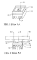
- the enclosure 14 typically comprises a material with a low coefficient of thermal expansion to match that of the semiconductor material of the integrated circuit 10. In addition, the enclosure must provide protection against moisture and other atmospheric conditions. The enclosure may also need to prevent interference between internal and external signals.
- the heat sink 18 typically comprises a material having a high thermal conductivity and, typically, including heat dissipating fins 24. However, the heat sink 18 and enclosure 14 may have very dissimilar coefficients of thermal expansion. During thermal cycling events, wherein the temperature of the structure rises and falls by a substantial amount, large thermal stresses are created in the adhesive layer 22. Thermal cracking may occur in the adhesive layer 22 due to this thermal cycling.
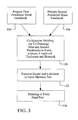
- FIG. 2 a cross sectional view of a prior art enclosure 34 with a heat sink 42 attached using an adhesive layer 38 is illustrated.
- the enclosure is attached to a printed circuit board (PCB) 50.
- PCB printed circuit board
- the integrated circuit chip 30 is sealed with a glass layer 54.
- Optical fiber 46 is connected to the chip 30 through the enclosure 34.
- Japanese Patent 7,321,261A discloses a low-cost tungsten alloy heat sink.
- the complex shaped, tungsten alloy heat sink demonstrates good heat radiation and thermal conductivity.
- the heat sink must still be bonded to the electronic device to function effectively.
- U.S. Patent 5,878,322 and U.S. Patent 5,886,407 disclose heat sinks for microelectronics packages that are formed using powder compacting. However, an adhesive is still needed to bond the heat sink to the enclosure.
- U.S. Patent 6,075,701 discloses an electronic structure having an embedded pyrolytic graphite heat sink material to enhance the heat dissipating performance.
- the processing parameters limit the range of materials that may be used for the enclosure, or casing. Only low melting point metals, such as aluminum, are compatible with the hot isostatic pressing process. Further, additional heat treatment processing, such as quenching and aging, must be performed to achieve optimum performance.
- a principal object of the present invention is to provide an effective and very manufacturable method to form an enclosure for a semiconductor device.
- a further object of the present invention is to provide a method for forming an enclosure combined with a heat sink, without a adhesive layer therebetween, to reduce cost and to improve reliability.
- a still further object of the present invention is to provide a method to form a combined enclosure and heat sink while maintaining low thermal expansion in the enclosure and high thermal conductivity in the heat sink.
- Another further object of the present invention is to provide a method to form a combined enclosure and heat sink where a hollow, cooling channel is formed in the heat sink to further improve the heat sink thermal conductivity.
- Another still further object of the present invention is to provide a method to form a combined enclosure and heat sink with a hollow, cooling channel where the cooling channel is formed by the same sintering process used to form the combined structure.
- Another object of the present invention is to provide an improved enclosure and heat sink structure.
- a method to form a combined enclosure and heat sink structure for a semiconductor device is achieved.
- a first feedstock comprising a first mixture of powdered metal materials, lubricants, and binders is prepared.
- a second feedstock comprising a second mixture of powdered metal materials, lubricants, and binders is prepared such that the difference between the sintering shrinkage of each of the first and second feedstocks is less than 1%.
- the first and second feedstocks are pressed to form a first green part having an enclosure shape and a second green part having a heat sink shape.
- the lubricants and the binders from the first and second green parts are removed to form a first powdered skeleton and a second powdered skeleton.
- the first and second powdered skeletons are sintered to complete the combined enclosure and heat sink structure.
- the first and second powdered skeletons are in intimate contact during the sintering.
- at least one hollow cooling channel is formed in the combine structure by burning away a fugitive plastic structure during the sintering process.
- the preferred embodiments disclose a novel combined enclosure and heat sink for a semiconductor device of the present invention.
- a method of forming a combined enclosure and heat sink structure comprising two materials is achieved. The two materials are formed and adjoined using a novel sintering process without use of an adhesive layer.
- An embodiment of the method and structure includes a means of creating hollow, cooling channels in the heat sink to further improve performance. It should be clear to those experienced in the art that the present invention can be applied and extended without deviating from the scope of the present invention.
- the first mixture of powdered materials preferably comprises one or more materials selected from the group consisting of: nickel, cobalt, iron, molybdenum, stainless steel, tungsten, tungsten-copper, molybdenum, molybdenum-copper, aluminum, aluminum nitride, alumina, and Kovar.
- Kovar is a trademark of Carpenter, Inc., and has a chemical composition of about 30% nickel, about 15% cobalt, and the balance iron.
- This first mixture of powdered materials is combined with lubricants and binders to form the first feedstock in step 100.
- any organic material which will decompose under elevated temperatures without leaving a residue that will be detrimental to the properties of the metal articles, can be used.
- Preferred materials are various organic polymers, such as stearic acids, micropulvar wax, paraffin wax, and polyethylene.
- Stearic acid particularly serves as a lubricant while all the other materials may be used as binders. It important to note that the amount and nature of the binder and lubricant that is added to the powder will determine the viscosity of the feedstock and the amount of shrinkage that will occur during the subsequent sintering step.
- the second mixture of powdered materials, prepared in step 104 will be subsequently formed into a heat sink for the combined enclosure and heat sink structure.
- the second mixture of powdered materials is therefore selected to display a second set of properties, and more particularly, a high thermal conductivity to pull heat generated in the integrated circuit away from the IC device.
- the second mixture of powdered materials exhibits a coefficient of thermal conductivity of between about 50 W/mK and about 450 W/mK in the final structure.
- the shrinkage of the enclosure and the heat sink, during sintering must be closely matched.
- the enclosure and the heat sink shrinkage cannot differ, one from another, by more than a critical amount.
- the amount that the feedstocks shrink after sintering differs, one from the other, by less than about 1%.
- the powdered materials used to form the first and second feedstocks in steps 100 and 104 must share similar characteristics such as particle shape, texture, and size distribution.
- the tap sizes of the two powders should not differ by more than about 30% while the mean particle size for both powders should be in the range of between about 1 micron and 40 microns.
- the first and second feedstocks are co-injected into a mold to form a green, combined enclosure and heat sink structure in step 108.
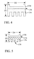
- the green, combined enclosure and heat sink structure is shown in cross section.
- the enclosure part 150 of the structure comprises the first feedstock molded and pressed into the enclosure shape.
- the heat sink part 154 of the structure comprises the second feedstock molded and pressed into the heat sink shape.
- the enclosure 150 and heat sink 154 are in intimate contact with one another along the boundary shown by 158.
- the heat sink section 174 of the first preferred embodiment structure comprises a fin design that extends the width of the structure.
- the enclosure 170 comprises a structural box with an opening into which the integrated circuit can be placed and bonded.
- a sealant and/or encapsulating cover can then be placed over the opening in the enclosure if needed.
- the heat sink 174 is permanently bonded to the enclosure 170 by the novel process.
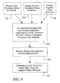
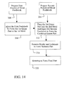
- Figs. 9 through 13 illustrate a third preferred embodiment of the present invention, showing a method of forming a hollow, cooling channel in the combined enclosure and heat sink. Referring particularly now to Fig. 9, this method is shown.
- the first and second feedstocks are prepared in steps 250 and 254.
- the preparation steps for the first and second feedstocks are substantially the same as in the first embodiment.
- the first feedstock will be subsequently formed into the enclosure, while the second feedstock will be formed into the heat sink.
- the novel method of the present invention utilizes a fugitive plastic structure to achieve the hollow, cooling channel.
- This fugitive plastic structure is prepared in step 258.
- a fugitive plastic structure is shown as 208.
- This structure comprises a material that can first be impregnated into the feedstock in a predictable spatial arrangement. The fugitive plastic structure then needs to maintain its shape during the molding and pressing step. Finally, the fugitive plastic structure must be capable of being vaporized, or burned away, during the sintering step without leaving a residue. Once burned away, the hollow, cooling channel remains where the fugitive plastic structure had been.
- the fugitive plastic structure preferably comprises a plastic material selected from the group consisting of: thermosetting polymers, thermoplastic polymers, cellulose, wax, gelatin, and glycol.
- the fugitive plastic structure may be prepared in step 258 using any of the methods well known in the art to form plastic parts, including, for example, plastic injection molding.
- the first and second feedstocks and the fugitive plastic structure are co-injected into a mold to form a green, combined enclosure and heat sink structure in step 262.
- any of the other methods herein disclosed will work as long as the plastic can be encapsulated in the enclosure, in the heat sink, or in both, prior to the sintering step.
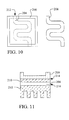
- a top view of the green, combined enclosure and heat sink structure is shown as 200, 204, and 212.
- the top view shows the green, enclosure section 200.
- a fugitive plastic structure 208 is impregnated into the heat sink and shown in hidden view as 204.
- the fugitive plastic structure 204 crosses the combined enclosure and heat sink structure.
- two endpoints of the fugitive plastic structure 204 are exposed at the exterior surface of the heat sink shape as shown by detail 212.
- a fugitive plastic structure 204 having multiple endpoints or a more complex shape, could be used.
- the combined enclosure and heat sink structure comprises an enclosure 220 comprising a first material and a heat sink 224 comprising a second material.
- the enclosure 220 and the heat sink 224 are coupled together by a sintering process.
- the combined enclosure and heat sink structure contains at least one, hollow, cooling channel 228.
- the hollow, cooling channel 228 extends to the edges 232 of the heat sink 224 to provide inlet and outlet points for fluid flow.
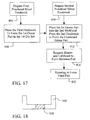
- a sixth preferred embodiment of the present invention is shown where a first and a second skeleton part are formed separately and then fixtured together during sintering.
- a first feedstock comprising a first mixture of powdered metal materials, lubricants, and binders is prepared in step 360.
- a second feedstock comprising a second mixture of powdered metal materials, lubricants, and binders is prepared in step 364. The difference between the sintering shrinkage of first and second feedstock is less than 1%.
- the first feedstock is injected into a first mold. Thereafter, the first feedstock is pressed to form a first green part having an enclosure shape in step 368.
- the second feedstock is injected into a second mold.
Landscapes
- Engineering & Computer Science (AREA)
- Manufacturing & Machinery (AREA)
- Mechanical Engineering (AREA)
- Chemical & Material Sciences (AREA)
- Composite Materials (AREA)
- Materials Engineering (AREA)
- Cooling Or The Like Of Semiconductors Or Solid State Devices (AREA)
- Powder Metallurgy (AREA)
Applications Claiming Priority (2)
| Application Number | Priority Date | Filing Date | Title |
|---|---|---|---|
| US940049 | 2001-08-27 | ||
| US09/940,049 US6569380B2 (en) | 2001-08-27 | 2001-08-27 | Enclosure for a semiconductor device |
Publications (2)
| Publication Number | Publication Date |
|---|---|
| EP1296370A2 true EP1296370A2 (de) | 2003-03-26 |
| EP1296370A3 EP1296370A3 (de) | 2006-05-17 |
Family
ID=25474132
Family Applications (1)
| Application Number | Title | Priority Date | Filing Date |
|---|---|---|---|
| EP02392015A Withdrawn EP1296370A3 (de) | 2001-08-27 | 2002-08-26 | Gehäuse für Halbleitervorrichtung |
Country Status (4)
| Country | Link |
|---|---|
| US (1) | US6569380B2 (de) |
| EP (1) | EP1296370A3 (de) |
| JP (2) | JP4146136B2 (de) |
| SG (1) | SG111930A1 (de) |
Cited By (3)
| Publication number | Priority date | Publication date | Assignee | Title |
|---|---|---|---|---|
| EP2233232A1 (de) * | 2009-03-20 | 2010-09-29 | Pratt & Whitney Canada Corp. | Verfahren zum Verbinden von pulverspritzgegossenen Teilen |
| US9970318B2 (en) | 2014-06-25 | 2018-05-15 | Pratt & Whitney Canada Corp. | Shroud segment and method of manufacturing |
| CN110193605A (zh) * | 2018-02-26 | 2019-09-03 | 恩佐科技股份有限公司 | 液冷头结构及其制造方法 |
Families Citing this family (18)
| Publication number | Priority date | Publication date | Assignee | Title |
|---|---|---|---|---|
| US20050190810A1 (en) * | 2004-02-27 | 2005-09-01 | Stuart Butterworth | Contact-bonded optically pumped semiconductor laser structure |
| KR100609014B1 (ko) * | 2004-02-27 | 2006-08-03 | 삼성전자주식회사 | 박막 히트 스프레더 및 그의 제조 방법 |
| KR100629496B1 (ko) * | 2005-08-08 | 2006-09-28 | 삼성전자주식회사 | Led 패키지 및 그 제조방법 |
| DE102006032415A1 (de) * | 2005-09-30 | 2007-04-05 | Osram Opto Semiconductors Gmbh | Verfahren zur Herstellung eines strahlungsemittierenden Bauelements und strahlungsemittierendes Bauelement |
| JP2007301808A (ja) * | 2006-05-10 | 2007-11-22 | Toshiba Tec Corp | ベース製造方法、ベース、およびヘッドモジュール |
| US20080011453A1 (en) * | 2006-07-12 | 2008-01-17 | Robert Liang | Heat-Dissipating Device For Memory And Method For Manufacturing The Same |
| WO2010065035A1 (en) * | 2008-12-04 | 2010-06-10 | Hewlett-Packard Development Company, L.P. | Carbon laminated enclosure |
| US7903418B2 (en) | 2009-04-21 | 2011-03-08 | Hewlett-Packard Development Company, L.P. | Thermal mitigation device and method |
| CA2797746C (en) * | 2009-04-29 | 2021-12-07 | Maetta Sciences Inc. | A method for co-processing components in a metal injection molding process, and components made via the same |
| CN102009175B (zh) * | 2010-10-08 | 2013-08-21 | 李亚东 | 一种多层壳芯复合结构零件的制备方法 |
| DE102012206087A1 (de) * | 2012-04-13 | 2013-10-17 | Rolls-Royce Deutschland Ltd & Co Kg | Verfahren zur Herstellung eines Bauteils eines Flugtriebwerks durch Metallpulverspritzgießen |
| DE102012014813B9 (de) | 2012-07-26 | 2016-06-16 | Wieland-Werke Ag | Strukturierte Kühlkörper in Modulbauweise |
| FR3035808B1 (fr) * | 2015-05-04 | 2021-01-29 | Snecma | Procede de fabrication d'une piece a partir d'elements fabriques par mise en forme d'un melange de poudre de metal ou de ceramique et d'au moins un liant |
| CN107008909A (zh) * | 2017-03-27 | 2017-08-04 | 刘金财 | 一种高精度粉末冶金齿轮的制备方法 |
| CN109676141B (zh) * | 2017-12-06 | 2020-10-23 | 全亿大科技(佛山)有限公司 | 异形复杂金属制品的制造方法及异形复杂金属制品 |
| CN108213409A (zh) * | 2018-01-17 | 2018-06-29 | 河北中瓷电子科技有限公司 | 电子封装用可伐合金墙体的制备方法 |
| DE102018121902A1 (de) * | 2018-09-07 | 2020-03-12 | Isabellenhütte Heusler Gmbh & Co. Kg | Herstellungsverfahren für ein elektrisches Widerstandselement und entsprechendes Widerstandselement |
| CN115815604A (zh) * | 2022-11-17 | 2023-03-21 | 大连藏龙光电子科技有限公司 | 一种提高光电器件封装可靠性的方法 |
Citations (8)
| Publication number | Priority date | Publication date | Assignee | Title |
|---|---|---|---|---|
| JPS59158538A (ja) | 1983-02-28 | 1984-09-08 | Ngk Spark Plug Co Ltd | 熱放散性を向上したicパツケ−ジ |
| GB2180409A (en) | 1983-02-14 | 1987-03-25 | Jr Raymond E Wiech | Method of forming multilayer ceramic substrates |
| JPH07321261A (ja) | 1994-05-27 | 1995-12-08 | Seiko Epson Corp | 半導体用ヒートシンク |
| WO1999003624A1 (en) | 1997-07-16 | 1999-01-28 | The Dow Chemical Company | A method to form dense complex shaped articles |
| US5878322A (en) | 1993-04-14 | 1999-03-02 | Polese; Frank J. | Heat-dissipating substrate for micro-electronic devices and fabrication method |
| US5886407A (en) | 1993-04-14 | 1999-03-23 | Frank J. Polese | Heat-dissipating package for microcircuit devices |
| US5972737A (en) | 1993-04-14 | 1999-10-26 | Frank J. Polese | Heat-dissipating package for microcircuit devices and process for manufacture |
| US6075701A (en) | 1999-05-14 | 2000-06-13 | Hughes Electronics Corporation | Electronic structure having an embedded pyrolytic graphite heat sink material |
Family Cites Families (7)
| Publication number | Priority date | Publication date | Assignee | Title |
|---|---|---|---|---|
| US4722824A (en) * | 1986-06-04 | 1988-02-02 | Fine Particle Technology Corp. | Method of joining green bodies prior to sintering |
| US5393484A (en) * | 1991-10-18 | 1995-02-28 | Fujitsu Limited | Process for producing sintered body and magnet base |
| JP3176152B2 (ja) * | 1992-10-30 | 2001-06-11 | 京セラ株式会社 | 半導体素子収納用パッケージの製造方法 |
| US6033788A (en) * | 1996-11-15 | 2000-03-07 | Case Western Reserve University | Process for joining powder metallurgy objects in the green (or brown) state |
| CA2232517C (en) * | 1997-03-21 | 2004-02-17 | Honda Giken Kogyo Kabushiki Kaisha .) | Functionally gradient material and method for producing the same |
| US6114048A (en) * | 1998-09-04 | 2000-09-05 | Brush Wellman, Inc. | Functionally graded metal substrates and process for making same |
| US6322746B1 (en) * | 1999-06-15 | 2001-11-27 | Honeywell International, Inc. | Co-sintering of similar materials |
-
2001
- 2001-08-27 US US09/940,049 patent/US6569380B2/en not_active Expired - Fee Related
-
2002
- 2002-02-22 SG SG200200946A patent/SG111930A1/en unknown
- 2002-02-22 JP JP2002045988A patent/JP4146136B2/ja not_active Expired - Fee Related
- 2002-08-26 EP EP02392015A patent/EP1296370A3/de not_active Withdrawn
-
2008
- 2008-04-11 JP JP2008103075A patent/JP2008223142A/ja active Pending
Patent Citations (8)
| Publication number | Priority date | Publication date | Assignee | Title |
|---|---|---|---|---|
| GB2180409A (en) | 1983-02-14 | 1987-03-25 | Jr Raymond E Wiech | Method of forming multilayer ceramic substrates |
| JPS59158538A (ja) | 1983-02-28 | 1984-09-08 | Ngk Spark Plug Co Ltd | 熱放散性を向上したicパツケ−ジ |
| US5878322A (en) | 1993-04-14 | 1999-03-02 | Polese; Frank J. | Heat-dissipating substrate for micro-electronic devices and fabrication method |
| US5886407A (en) | 1993-04-14 | 1999-03-23 | Frank J. Polese | Heat-dissipating package for microcircuit devices |
| US5972737A (en) | 1993-04-14 | 1999-10-26 | Frank J. Polese | Heat-dissipating package for microcircuit devices and process for manufacture |
| JPH07321261A (ja) | 1994-05-27 | 1995-12-08 | Seiko Epson Corp | 半導体用ヒートシンク |
| WO1999003624A1 (en) | 1997-07-16 | 1999-01-28 | The Dow Chemical Company | A method to form dense complex shaped articles |
| US6075701A (en) | 1999-05-14 | 2000-06-13 | Hughes Electronics Corporation | Electronic structure having an embedded pyrolytic graphite heat sink material |
Cited By (5)
| Publication number | Priority date | Publication date | Assignee | Title |
|---|---|---|---|---|
| EP2233232A1 (de) * | 2009-03-20 | 2010-09-29 | Pratt & Whitney Canada Corp. | Verfahren zum Verbinden von pulverspritzgegossenen Teilen |
| US10226818B2 (en) | 2009-03-20 | 2019-03-12 | Pratt & Whitney Canada Corp. | Process for joining powder injection molded parts |
| US11383299B2 (en) | 2009-03-20 | 2022-07-12 | Pratt & Whitney Canada Corp. | Process for joining powder injection molded parts |
| US9970318B2 (en) | 2014-06-25 | 2018-05-15 | Pratt & Whitney Canada Corp. | Shroud segment and method of manufacturing |
| CN110193605A (zh) * | 2018-02-26 | 2019-09-03 | 恩佐科技股份有限公司 | 液冷头结构及其制造方法 |
Also Published As
| Publication number | Publication date |
|---|---|
| JP2003078083A (ja) | 2003-03-14 |
| US6569380B2 (en) | 2003-05-27 |
| SG111930A1 (en) | 2005-06-29 |
| JP4146136B2 (ja) | 2008-09-03 |
| JP2008223142A (ja) | 2008-09-25 |
| EP1296370A3 (de) | 2006-05-17 |
| US20030039571A1 (en) | 2003-02-27 |
Similar Documents
| Publication | Publication Date | Title |
|---|---|---|
| US6569380B2 (en) | Enclosure for a semiconductor device | |
| US6114048A (en) | Functionally graded metal substrates and process for making same | |
| US6238454B1 (en) | Isotropic carbon/copper composites | |
| US5533257A (en) | Method for forming a heat dissipation apparatus | |
| US5972737A (en) | Heat-dissipating package for microcircuit devices and process for manufacture | |
| US5886407A (en) | Heat-dissipating package for microcircuit devices | |
| EP0248258A2 (de) | Wärmesenke aus einer gemischten Metallegierung | |
| RU2216602C2 (ru) | Композиционный материал | |
| CN101649400A (zh) | 电子封装用金刚石增强金属基复合材料及其制备方法 | |
| US8080872B2 (en) | Surface mount package with high thermal conductivity | |
| CN100454525C (zh) | 复合材料及电路或电模块 | |
| EP1231633B1 (de) | Material für eine wärme-abführende platte auf der ein halbleiter montiert ist, herstellungsmethode und keramisches gehäuse,produziert unter verwendung derselben | |
| JP2005005528A (ja) | 半導体素子搭載用モジュール | |
| JP2004160549A (ja) | セラミックス−金属複合体およびこれを用いた高熱伝導放熱用基板 | |
| TWI640495B (zh) | 複合構件及其用途與製作方法 | |
| JP3451979B2 (ja) | 半導体装置 | |
| JP4227610B2 (ja) | 放熱基体の製造方法 | |
| JPH07105464B2 (ja) | 半導体素子搭載用半導体装置 | |
| JP2967065B2 (ja) | 半導体モジュール | |
| JP3552587B2 (ja) | 複合材料及び半導体装置 | |
| JP3180100B2 (ja) | 半導体モジュール | |
| WO1997027626A1 (en) | Integrated circuit package having enhanced heat dissipation and grounding | |
| CN115692216B (zh) | 一种异种材质复合成型的电子封装结构及其制备方法 | |
| JP2003318316A (ja) | セラミックス回路基板 | |
| JP3850312B2 (ja) | 半導体素子収納用パッケージおよび半導体装置 |
Legal Events
| Date | Code | Title | Description |
|---|---|---|---|
| PUAI | Public reference made under article 153(3) epc to a published international application that has entered the european phase |
Free format text: ORIGINAL CODE: 0009012 |
|
| AK | Designated contracting states |
Kind code of ref document: A2 Designated state(s): AT BE BG CH CY CZ DE DK EE ES FI FR GB GR IE IT LI LU MC NL PT SE SK TR Designated state(s): AT BE BG CH CY CZ DE DK EE ES FI FR GB GR IE IT LI LU MC NL PT SE SK TR |
|
| AX | Request for extension of the european patent |
Extension state: AL LT LV MK RO SI |
|
| PUAL | Search report despatched |
Free format text: ORIGINAL CODE: 0009013 |
|
| AK | Designated contracting states |
Kind code of ref document: A3 Designated state(s): AT BE BG CH CY CZ DE DK EE ES FI FR GB GR IE IT LI LU MC NL PT SE SK TR |
|
| AX | Request for extension of the european patent |
Extension state: AL LT LV MK RO SI |
|
| 17P | Request for examination filed |
Effective date: 20061116 |
|
| AKX | Designation fees paid |
Designated state(s): AT BE BG CH CY CZ DE DK EE ES FI FR GB GR IE IT LI LU MC NL PT SE SK TR |
|
| 17Q | First examination report despatched |
Effective date: 20090325 |
|
| STAA | Information on the status of an ep patent application or granted ep patent |
Free format text: STATUS: THE APPLICATION IS DEEMED TO BE WITHDRAWN |
|
| 18D | Application deemed to be withdrawn |
Effective date: 20150303 |