EP1297385B1 - Material und verfahren für die herstellung eines elektrisch leitfähigen musters - Google Patents
Material und verfahren für die herstellung eines elektrisch leitfähigen musters Download PDFInfo
- Publication number
- EP1297385B1 EP1297385B1 EP01978242A EP01978242A EP1297385B1 EP 1297385 B1 EP1297385 B1 EP 1297385B1 EP 01978242 A EP01978242 A EP 01978242A EP 01978242 A EP01978242 A EP 01978242A EP 1297385 B1 EP1297385 B1 EP 1297385B1
- Authority
- EP
- European Patent Office
- Prior art keywords
- outermost layer
- exposed
- exposure
- light
- group
- Prior art date
- Legal status (The legal status is an assumption and is not a legal conclusion. Google has not performed a legal analysis and makes no representation as to the accuracy of the status listed.)
- Expired - Lifetime
Links
Classifications
-
- G—PHYSICS
- G03—PHOTOGRAPHY; CINEMATOGRAPHY; ANALOGOUS TECHNIQUES USING WAVES OTHER THAN OPTICAL WAVES; ELECTROGRAPHY; HOLOGRAPHY
- G03F—PHOTOMECHANICAL PRODUCTION OF TEXTURED OR PATTERNED SURFACES, e.g. FOR PRINTING, FOR PROCESSING OF SEMICONDUCTOR DEVICES; MATERIALS THEREFOR; ORIGINALS THEREFOR; APPARATUS SPECIALLY ADAPTED THEREFOR
- G03F7/00—Photomechanical, e.g. photolithographic, production of textured or patterned surfaces, e.g. printing surfaces; Materials therefor, e.g. comprising photoresists; Apparatus specially adapted therefor
- G03F7/004—Photosensitive materials
- G03F7/016—Diazonium salts or compounds
- G03F7/0166—Diazonium salts or compounds characterised by the non-macromolecular additives
-
- G—PHYSICS
- G03—PHOTOGRAPHY; CINEMATOGRAPHY; ANALOGOUS TECHNIQUES USING WAVES OTHER THAN OPTICAL WAVES; ELECTROGRAPHY; HOLOGRAPHY
- G03F—PHOTOMECHANICAL PRODUCTION OF TEXTURED OR PATTERNED SURFACES, e.g. FOR PRINTING, FOR PROCESSING OF SEMICONDUCTOR DEVICES; MATERIALS THEREFOR; ORIGINALS THEREFOR; APPARATUS SPECIALLY ADAPTED THEREFOR
- G03F7/00—Photomechanical, e.g. photolithographic, production of textured or patterned surfaces, e.g. printing surfaces; Materials therefor, e.g. comprising photoresists; Apparatus specially adapted therefor
- G03F7/004—Photosensitive materials
-
- G—PHYSICS
- G03—PHOTOGRAPHY; CINEMATOGRAPHY; ANALOGOUS TECHNIQUES USING WAVES OTHER THAN OPTICAL WAVES; ELECTROGRAPHY; HOLOGRAPHY
- G03F—PHOTOMECHANICAL PRODUCTION OF TEXTURED OR PATTERNED SURFACES, e.g. FOR PRINTING, FOR PROCESSING OF SEMICONDUCTOR DEVICES; MATERIALS THEREFOR; ORIGINALS THEREFOR; APPARATUS SPECIALLY ADAPTED THEREFOR
- G03F7/00—Photomechanical, e.g. photolithographic, production of textured or patterned surfaces, e.g. printing surfaces; Materials therefor, e.g. comprising photoresists; Apparatus specially adapted therefor
- G03F7/004—Photosensitive materials
- G03F7/016—Diazonium salts or compounds
- G03F7/0163—Non ionic diazonium compounds, e.g. diazosulphonates; Precursors thereof, e.g. triazenes
-
- G—PHYSICS
- G03—PHOTOGRAPHY; CINEMATOGRAPHY; ANALOGOUS TECHNIQUES USING WAVES OTHER THAN OPTICAL WAVES; ELECTROGRAPHY; HOLOGRAPHY
- G03F—PHOTOMECHANICAL PRODUCTION OF TEXTURED OR PATTERNED SURFACES, e.g. FOR PRINTING, FOR PROCESSING OF SEMICONDUCTOR DEVICES; MATERIALS THEREFOR; ORIGINALS THEREFOR; APPARATUS SPECIALLY ADAPTED THEREFOR
- G03F7/00—Photomechanical, e.g. photolithographic, production of textured or patterned surfaces, e.g. printing surfaces; Materials therefor, e.g. comprising photoresists; Apparatus specially adapted therefor
- G03F7/004—Photosensitive materials
- G03F7/09—Photosensitive materials characterised by structural details, e.g. supports, auxiliary layers
- G03F7/093—Photosensitive materials characterised by structural details, e.g. supports, auxiliary layers characterised by antistatic means, e.g. for charge depletion
-
- H—ELECTRICITY
- H05—ELECTRIC TECHNIQUES NOT OTHERWISE PROVIDED FOR
- H05K—PRINTED CIRCUITS; CASINGS OR CONSTRUCTIONAL DETAILS OF ELECTRIC APPARATUS; MANUFACTURE OF ASSEMBLAGES OF ELECTRICAL COMPONENTS
- H05K3/00—Apparatus or processes for manufacturing printed circuits
- H05K3/10—Apparatus or processes for manufacturing printed circuits in which conductive material is applied to the insulating support in such a manner as to form the desired conductive pattern
- H05K3/105—Apparatus or processes for manufacturing printed circuits in which conductive material is applied to the insulating support in such a manner as to form the desired conductive pattern by conversion of non-conductive material on or in the support into conductive material, e.g. by using an energy beam
Definitions
- the present invention relates to a material and a method for making an electroconductive pattern.
- ITO indium-tin oxide
- plastic resins as a substrate and organic electroconductive polymer layers as electrodes.
- plastic electronics allow the realization of low cost devices with new properties ( Physics World, March 1999, p.25-39 ).
- Flexible plastic substrates can be provided with an electroconductive polymer layer by continuous roller coating methods (compared to batch process such as sputtering) and the resulting organic electrodes enable the fabrication of electronic devices characterised by a higher flexibility and a lower weight.
- electroconductive polymers such as polypyrrole, polyaniline, polyacetylene, polyparaphenylene, polythiophene, polyphenylenevinylene, polythienylenevinylene and polyphenylenesulphide are known in the art.
- EP-A 440 957 discloses dispersions of polythiophenes, constructed from structural units of formula (I): in which R 1 and R 2 independently of one another represent hydrogen or a C 1-4 -alkyl group or together form an optionally substituted C 1-4 -alkylene residue, in the presence of polyanions.
- EP-A-686 662 discloses mixtures of A) neutral polythiophenes with the repeating structural unit of formula (I), in which R 1 and R 2 independently of one another represent hydrogen or a C1-C4 alkyl group or together represent an optionally substituted C1-C4 alkylene residue, preferably an optionally with alkyl group substituted methylene, an optionally with C1-C12-alkyl or phenyl group substituted 1,2-ethylene residue or a 1,2-cyclohexene residue, and B) a di- or polyhydroxy- and/or carboxy groups or amide or lactam group containing organic compound; and conductive coatings therefrom which are tempered at elevated temperature, preferably between 100 and 250 °C, during preferably 1 to 90 seconds to increase their resistance preferably to ⁇ 300 ohm/square.
- R 1 and R 2 independently of one another represent hydrogen or a C1-C4 alkyl group or together represent an optionally substituted C1-C4 alkylene residue, preferably an
- EP-A 614 123 discloses a water-soluble electrically conductive composition of matter comprising a polyacid and a polymer comprising at least one conjugated region composed of repeating units which contain a conjugated basic atom.
- water-soluble electrically conductive polymer comprising at least one conjugated region composed of repeating units which contain a conjugated basic atom
- only polyaniline and substituted polyanilines are exemplified.
- EP-A 382 046 discloses an electrically conductive resist material, essentially comprising at least one ionic radiation-sensitive polymer and a soluble electrically conductive oligomer or a soluble electrically conductive polymer. Polymers of substituted thiophenes are exemplified, but no specific ionic radiation-sensitive polymers.
- EP-A 338 786 discloses a negative working, photosensitive, overlay color proofing film which comprises, in order: (i) a transparent substrate; (ii) a photosensitive layer on the substrate, which photosensitive layer comprises a light sensitive, negative working, polymeric diazonium compound which is the polycondensation product of 3-methoxy-4-diazodiphenylamine sulfate and 4,4'-bis-methoxymethyl diphenyl ether precipitated as the chloride salt, which diazonium compound is present in sufficient amount to photosensitize the layer; and a water insoluble, water swellable binder resin in sufficient amount to bind the layer components in a uniform film; and at least one colorant in sufficient amount to uniformly color the layer; wherein upon imagewise exposure of the photosensitive layer to sufficient actinic radiation the film is capable of being developed with water alone.
- Coated layers of organic electroconductive polymers can be structured into patterns using known microlithography techniques.
- WO-A - 97 18944 a process is described wherein a positive or negative photoresist is applied on top of a coated layer of an organic electroconductive polymer, and after the steps of selectively exposing the photoresist to UV light, developing the photoresist, etching the electroconductive polymer layer and finally stripping the non-developed photoresist with an organic solvent, a patterned layer is obtained.
- a similar technique has been described in 1988 in Synthetic Metals, volume 22, pages 265-271 for the design of an all-organic thin-film transistor. Such methods are cumbersome as they involve many steps and require the use of hazardous chemicals.
- An electroconductive pattern can be realized with the materials of the present invention, which are optionally conductivity enhanced, by pattern-wise exposure, with or without a subsequent single wet processing step, and optional conductivity enhancement. No etching liquids or organic solvents are required.
- the aspects of the present invention are realized by a material for making an electroconductive pattern, the material comprising a support and a light-exposure differentiable element, wherein the light-exposure differentiable element comprises an outermost layer containing a polyanion and a polymer or copolymer of a substituted or unsubstituted thiophene, and optionally a second layer contiguous with the outermost layer; and wherein the outermost layer and/or the optional second layer contains a light-sensitive component capable upon exposure of changing the removability of the exposed parts of the outermost layer relative to the unexposed parts of the outermost layer, characterized in that the light-sensitive component is a multidiazonium salt, a resin comprising a diazonium salt or a quinonediazide compound.
- the light-sensitive component is a multidiazonium salt, a resin comprising a diazonium salt or a quinonediazide compound.
- support means a “self-supporting material” so as to distinguish it from a “layer” which may be coated on a support, but which is itself not self-supporting. It also includes any treatment necessary for, or layer applied to aid, adhesion to the light-exposure differentiable element:
- electroconductive means having a surface resistivity below 10 6 ⁇ /square.
- Antistatic materials have surface resistivities in the range from 10 6 to 10 11 ⁇ /square and cannot be used as an electrode.
- electroconductive pattern means a pattern made up by the non-removed areas of the outermost layer, according to the present invention, which are electroconductive or can be made electroconductive by post-treatment.
- Conductivity enhancement refers to a process in which the conductivity is enhanced e.g. by contact with high boiling point liquids such as di- or polyhydroxy- and/or carboxy groups or amide or lactam group containing organic compound optionally followed by heating at elevated temperature, preferably between 100 and 250 °C, during preferably 1 to 90 seconds, results in conductivity increase.
- high boiling point liquids such as di- or polyhydroxy- and/or carboxy groups or amide or lactam group containing organic compound optionally followed by heating at elevated temperature, preferably between 100 and 250 °C, during preferably 1 to 90 seconds, results in conductivity increase.
- aprotic compounds with a dielectric constant ⁇ 15, e.g. N-methyl-pyrrolidinone temperatures below 100°C can be used.
- Such conductivity enhancement is observed with polythiophenes and can take place during the preparation of the outermost layer or subsequently.
- Particularly preferred liquids for such treatment are N-methyl-pyrrolidinone and diethylene glycol such as disclosed in EP
- removability means mechanically removable in the absence of a liquid or removable with the application of a liquid with or without the simultaneous or subsequent use of rubbing or other mechanical removal means.
- the application of liquid can dissolve, swell or disperse the outermost layer according to the present invention such that removal is realized or enabled.
- light-exposure differentiable element means an element which upon light exposure produces changes in the properties or composition of the exposed parts of the element with respect to the properties or composition.of the unexposed parts of the element.
- the term surface resistivity ratio means the ratio of the surface resistivity of the parts (areas) of the light-exposure differentiable element from which parts (areas) of the outermost layer, according to.the invention, have been removed to that of the parts (areas) of the light-exposure differentiable element from which no parts (areas) of the outermost layer, according to the invention, have been removed, after treatment to enhance the conductivity of the non-removed parts (areas) of the outermost layer if this is required to increase (enhance) the conductivity of the non-removed parts (areas) of the outermost layer.
- surface resistivity ratio means the ratio of the surface resistivity of the exposed parts (areas) of the outermost layer to that of the non-exposed parts (areas) of the outermost layer.
- the material for making an electroconductive pattern need not itself be electroconductive as long as patterns produced with such a material can be rendered electroconductive by a post-treatment process, such as a conductivity enhancement process. Furthermore, no material need be removed from the outermost layer containing a polymer or copolymer of a substituted or unsubstituted thiophene, according to the present invention, in order to realize an electroconductive pattern, after optional processing to remove the residual light-sensitive component, as long as differential removability subsequent to exposure is feasible. In this case the light-sensitive component present is capable upon exposure of realizing this effect as well as changing the removability of the exposed parts of the outermost layer relative to the unexposed parts of the outermost layer.
- the optional second layer must be between the outermost layer and the support as it cannot be the outermost layer.
- the polymer or copolymer of a substituted or unsubstituted thiophene is water-dispersible.
- electroconductive is related to the electric resistivity of the material.
- the electric resistivity of a layer is generally expressed in terms of surface resistivity R s (unit ⁇ ; often specified as ⁇ /square).
- the support coated with the electroconductive outermost layer is cut to obtain a strip having a length of 27.5 cm and a width of 35 mm and strip electrodes are applied over its width at a distance of 10 cm perpendicular to the edge of the strip.
- the electrodes are made of an electroconductive polymer, ECCOCOAT CC-2 available from Emerson & Cumming Speciality polymers.
- ECCOCOAT CC-2 available from Emerson & Cumming Speciality polymers.
- Over the electrode a constant potential is applied and the current flowing through the circuit is measured on a pico-amperometer KEITHLEY 485. From the potential and the current, taking into account the geometry of the area between the electrodes, the surface resistivity in ⁇ /square is calculated.
- the surface resistivity was measured by contacting the outermost layer with parallel copper electrodes each 35 mm long and 35 mm apart capable of forming line contacts, the electrodes being separated by a teflon insulator. This enables a direct measurement of the surface resistivity.
- Supports for use according to the present invention include polymeric films, silicon, ceramics, oxides, glass, polymeric film reinforced glass, glass/plastic laminates, metal/plastic laminates, paper and laminated paper, optionally treated, provided with a subbing layer or other adhesion promoting means to aid adhesion to the light-exposure differentiable element.
- Suitable polymeric films are poly(ethylene terephthalate), poly(ethylene naphthalate), polystyrene, polyethersulphone, polycarbonate, polyacrylate,' polyamide, polyimides, cellulosetriacetate, polyolefins and polyvinylchloride, optionally treated by corona discharge or glow discharge or provided with a subbing layer.
- the support is treated with a corona discharge or a glow discharge.
- a corona discharge or a glow discharge enable the use of polymeric films as a support without a subbing layer.
- Such materials can be developed, optionally while softly rubbing, and still yield an excellent conductivity ratio between exposed and non-exposed areas.
- a light-exposure differentiable element is an element which upon light exposure produces changes in the properties or composition of the exposed parts of the element with respect to the properties.or composition of the unexposed parts of the element. Examples of such changes are exposure-induced crosslinking; exposure-induced increase or decrease of solubility; and exposure-induced increase or decrease of adhesion to the support.
- these changes in the properties or composition of the light-exposure differentiable element are due to the.presence of a light-sensitive component in the outermost layer and/or the second layer, which enables either the exposed or unexposed parts of the outermost layer to be removed, optionally with the assistance of a developer, i.e. the removability can either be rendered more (positive working) or less (negative working) removable by a developer upon exposure to light.
- the light-sensitive component capable upon exposure of changing the removability of the exposed parts of the outermost layer relative to the unexposed parts of the outermost layer is a multidiazonium salt or a resin comprising a diazonium salt, which reduces the removability of exposed parts of the outermost layer.
- Combinations of resins comprising a diazonium salt can also be used.
- the light-sensitive component is a multidiazonium salt or a resin comprising a diazonium salt, increasing the pH of the coating dispersions and solutions used in preparing the light-exposure differentiable element has been found to improve the shelf-life, i.e. retention of properties upon storage, of materials according to the present invention.' pH's between 2.5 and 9 are preferred, with pH's between 3 and 6 being particularly preferred. Such pH's can, for example, be realized by adding ammonium hydroxide.
- the light-sensitive component capable upon exposure of changing the removability of the exposed parts of the outermost layer relative to the unexposed parts of the outermost layer is a quinone diazide compound, which increases the removability of exposed parts of the outermost layer.
- the outermost layer has a surface resistivity lower than 10 6 ⁇ /square.
- the outermost layer has a surface resistivity lower than 10 4 ⁇ /square.
- the outermost layer has a surface resistivity capable of being lower than 10 6 ⁇ /square after treatment in a so-called conductivity enhancement process.
- the polymer of a substituted or unsubstituted thiophene corresponds to the formula (II): in which n is larger than 1 and each of R 1 and R 2 independently represents hydrogen or an optionally substituted C 1-4 alkyl group or together represent an optionally substituted C 1-4 alkylene group or an optionally substituted cycloalkylene group, preferably an ethylene group, an optionally alkyl-substituted methylene group, an optionally C 1-12 alkyl- or phenyl-substituted ethylene group, a 1,3-propylene group or a 1,2-cyclohexylene group.
- Stable aqueous polythiophene dispersions having a solids content of 0.05 to 55% by weight and preferably of 0.1 to 10% by weight can be obtained by dissolving thiophenes corresponding to the formula above, a polyacid and an oxidising agent in an organic solvent or preferably in water, optionally containing a certain amount of organic solvent, and then stirring the resulting solution or emulsion at 0°C to 100°C until the polymerisation reaction is completed.
- the polythiophenes formed by the oxidative polymerisation are positively charged, the location and number of such positive charges being not determinable with certainty and therefore not mentioned in the general formula of the repeating units of the polythiophene polymer.
- the oxidising agents are those which are typically used for the oxidative polymerisation of pyrrole as described in for example J. Am. Soc. 85, 454 (1963 ).
- Peferred inexpensive and easy-to-handle oxidising agents are iron(III) salts, e.g. FeCl 3 , Fe(ClO 4 ) 3 and the iron(III) salts of organic acids and inorganic acids containing organic residues.
- Other suitable oxidising agents are H 2 O 2 , K 2 Cr 2 O 7 , alkali or ammonium persulphates, alkali perborates, potassium permanganate and copper salts such as copper tetrafluoroborate.
- Air or oxygen can also be used as oxidising agents.
- the polyacid forms a polyanion or, alternatively, the polyanion can be added as a salt of the corresponding polyacids, e.g. an alkali salt.
- Preferred polyacids or salts thereof are polymeric carboxylic acids such as poly(acrylic acid), poly((meth)acrylic acid) and poly(maleic acid) or polymeric sulphonic acids such as poly(styrene sulphonic acid) or poly(vinyl sulphonic acid).
- copolymers of such carboxylic and/or sulphonic acids and of other polymerizable monomers such as styrene or acrylates can be used.
- the polyanion is poly(styrene sulphonate).
- the molecular weight of these polyanion forming polyacids is preferably between 1000 and 2x10 6 , more preferably between 2000 and 5x10 5 .
- These polyacids or their alkali salts are commercially available and can be prepared according to the known methods, e.g. as described in Houben-Weyl, Methoden der Organische Chemie, Bd. E20 Makromolekulare Stoffe, Mol 2, (1987), pp. 1141.
- the coating dispersion or solution of a polyanion and a polymers or copolymer of a substituted or unsubstituted thiophene can also comprise additional ingredients, such as one or more binders, one or more surfactants, spacing particles, UV-acutance compounds or IR-absorbers.
- the coating dispersion or solution of a polyanion and a polymer or copolymer of a substituted or unsubstituted thiophene preferably also comprises an organic compound that is: a linear, branched or cyclic aliphatic C 2-20 hydrocarbon or an optionally substituted aromatic C 6-14 hydrocarbon or a pyran or a furan, the organic compound comprising at least two hydroxy groups or at least one -COX or -CONYZ group wherein X denotes -OH and Y and Z independently of one another represent H or alkyl; or a heterocyclic compound containing at least one lactam group.
- organic compounds are e.g.
- sugar or sugar derivatives such as arabinose, saccharose, glucose, fructose and lactose, or di- or polyalcohols such as sorbitol, xylitol, mannitol, mannose, galactose, sorbose, gluconic acid, ethylene glycol, di- or tri(ethylene glycol), 1,1,1-trimethylol-propane, 1,3-propanediol, 1,5-pentanediol, 1,2,3-propantriol, 1,2,4-butantriol, 1,2,6-hexantriol, or aromatic di- or polyalcohols such as resorcinol.
- sugar or sugar derivatives such as arabinose, saccharose, glucose, fructose and lactose
- di- or polyalcohols such as sorbitol, xylitol, mannitol, mannose, galactose, sorbose, gluconic acid, ethylene glyco
- the light-exposure differentiable element containing a multidiazonium salt Upon exposure the light-exposure differentiable element containing a multidiazonium salt is converted from water removable to water unremovable (due to the destruction of the diazonium groups) and additionally the photolysis products of the diazo may increase the level of crosslinking of the polymeric binder or resin comprising a multidiazonium salt if present, thereby selectively converting the surface, into an image pattern, from removable to unremovable. The unexposed areas remain unchanged, i.e. removable. Combinations of multidiazonium salts can also be used.
- Bisdiazonium salts for use in the present invention include: benzidine tetrazoniumchloride, 3,3'-dimethylbenzidine tetrazoniumchloride, 3,3'-dimethoxybenzidine tetrazoniumchloride, 4,4'-diaminodiphenylamine tetrazoniumchloride, 3,3'-diethylbenzidine tetrazoniumsulphate, 4-aminodiphenylamine diazoniumsulphate, 4-aminodiphenylamine diazoniumchloride, 4-piperidino aniline diazoniumsulphate, 4-diethylamino aniline diazoniumsulphate and oligomeric condensation products of diazodiphenylamine and formaldehyde.
- the light-sensitive component capable upon exposure of changing the removability of the exposed parts of the outermost layer relative to the unexposed parts of the outermost layer is a bis(aryldiazosulphonate) salt, a tris(aryldiazosulphonate) salt or a tetrakis(aryldiazosulphonate) salt, which reduces the removability of exposed parts of the outermost layer.
- L preferably represents a substituted or unsubstituted divalent aryl group or a substituted or unsubstituted.saturated or unsaturated alkylene group, whose chain is optionally substituted with at least one of an oxygen atom, a sulphur atom or a nitrogen atom.
- Ar preferably represents an unsubstituted phenyl group or a phenyl group substituted with one or more alkyl groups, aryl groups, alkoxy groups, aryloxy groups or amino groups.
- M preferably represents a cation such as NH 4 + or a metal ion such as a cation of Al, Cu, Zn, an alkaline earth metal or alkali metal.
- Particularly suitable bis(aryldiazosulphonate) salts are: ⁇ max [nm] absorption of a 25ppm solution in water BADS01 308 0.785 BADS02 308 1.568 BADS03 -
- the light-sensitive component capable upon exposure of changing the removability of the exposed parts of the outermost layer relative to the unexposed parts of the outermost layer is a bis(aryldiazosulphonate) salt, which reduces the removability of exposed parts of the outermost layer, is selected from the group consisting of BADS01, BADS02 and BADS03.
- the aryldiazosulfonate according to formula (I) is selected from the group consisting of BADS01, BADS02 and BADS03.
- Resins comprising a diazonium salt
- Suitable resins comprising a diazonium salt, according to the present invention include polymers or copolymers of an aryldiazosulphonate and condensation products of an aromatic diazonium salt. Such condensation products are described, for example, in DE-P-1 214 086 .
- the light-exposure differentiable element containing resins comprising a diazonium salt are converted from removable to unremovable (due to the destruction of the diazonium groups) and additionally the photolysis products of the diazo may increase the level of crosslinking of the polymeric binder or resin comprising a diazonium salt, thereby selectively converting the surface, into an image pattern, from removable to unremovable.
- the unexposed areas remain unchanged, i.e. removable.
- the light-sensitive component capable upon exposure of changing the removability of the exposed parts of the outermost layer relative to the unexposed parts of the outermost layer is a polymer or copolymer of an aryldiazosulphonate, which reduces the removability of exposed parts of the outermost layer.
- the light-sensitive component capable upon exposure of changing the removability of the exposed parts of the outermost layer relative to the unexposed parts of the outermost layer is a polymer or copolymer of an aryldiazosulphonate, which reduces the removability of exposed parts of the outermost layer, represented by formula (III): wherein R 0 , R 1 and R 2 each independently represent hydrogen, an alkyl group, a nitrile or a halogen, e.g. Cl, L represents a divalent linking group, n represents 0 or 1, A represents an aryl group and M represents a cation.
- L preferably represents divalent linking group selected from the group consisting of: -(X) t -CONR 3 -, -(X) t -COO-, -X- and -(X) t -CO-, wherein t represents 0 or 1;
- R 3 represents hydrogen, an alkyl group or an aryl group;
- X represent an alkylene group, an arylene group, an alkylenoxy group, an arylenoxy group, an alkylenethio group, an arylenethio group, an alkylenamino group, an arylenamino group, oxygen, sulphur or an aminogroup.
- A preferably represents an unsubstituted aryl group, e.g.
- M preferably represents a cation such as NH 4 + or a metal ion such as a cation of Al, Cu, Zn, an alkaline earth metal or alkali metal.
- Polymers and copolymers of an aryldiazosulphonate can be prepared by homo- or copolymerization of aryldiazosulphonate monomers with other aryldiazosulphonate monomers and/or with vinyl monomers such as (meth)acrylic acid or esters thereof, (meth)acrylamide, acrylonitrile, vinylacetate, vinylchloride, vinylidene chloride, styrene, alpha-methyl styrene etc.'
- a particularly preferred comonomer is hydroxyethylmethacrylate.
- Suitable aryldiazosulphonate monomers for preparing such polymers and copolymers of an aryldiazosulphonate are: ADS-MONOMER 01 ADS-MONOMER 02 ADS-MONOMER 03 ADS-MONOMER 04 ADS-MONOMER 05 ADS-MONOMER 06 ADS-MONOMER 07 Specific examples of suitable aryldiazosulphonate polymers are described in EP-A-771 645 .
- Suitable resins comprising a diazonium salt are given below.
- NDP01 Negalux N18
- NDP04 homopolymer of ADS-MONOMER 01
- NDP05 hydroxyethylacrylate
- NDP06 methyl methacrylate
- NDP07 N-isopropyl-acrylamide
- NDP08 N-isopropyl-acrylamide, ADS-MONOMER 01 (80/20) copolymer
- NDP08 N-isopropyl-acrylamide
- the weight ratio of the polymer or copolymer of an aryldiazosulphonate to the polymer or copolymer of a substituted or unsubstituted thiophene is between 10:200 and 400:200.
- the light-sensitive component capable upon exposure of changing the removability of the exposed parts of the outermost layer relative to the unexposed parts of the outermost layer is a combination of a resin comprising an aryldiazosulphonate, which reduces the removability of exposed parts of the outermost layer, and a bis(aryldiazosulphonate) salt, which reduces the removability of exposed parts of the outermost layer.
- the light-sensitive component capable upon exposure of changing the removability of the exposed parts of the outermost layer relative to the unexposed parts of the outermost layer is a combination of a resin comprising an aryldiazosulphonate, which reduces the removability of exposed parts of the outermost layer, and a bis(aryldiazosulphonate) salt, which reduces the removability of exposed parts of the outermost layer, in the weight percentage ratio range of 60%/40% to 10%/90%.
- the light-sensitive component capable upon exposure of changing the removability of the exposed parts of the outermost layer relative to the unexposed parts of the outermost layer is a combination of a resin comprising an aryldiazosulphonate, which reduces the removability of exposed parts of the outermost layer, and a bis(aryldiazosulphonate) sat, which reduces the removability of exposed parts of the outermost layer, in the weight percentage ratio range of 50%/50% to 20%/80%.
- the light-sensitive component capable upon exposure of changing the removability of the exposed parts of the outermost layer relative.to the unexposed parts of the outermost layer is a combination of a copolymer of hydroxyethylmethacrylate and sodium-4-methacryloyl-aminophenyl-diazo-sulphonate, which reduces the removability of exposed parts of the outermost layer, and an bis(aryldiazosulphonate) salt, which reduces the removability of exposed parts of the outermost layer.
- the light-sensitive component capable upon exposure of changing the removability of the exposed parts of the outermost layer relative to the unexposed parts of the outermost layer is a quinonediazide compound, which increases the removability of exposed parts of the outermost layer.
- the light-sensitive component capable upon exposure of changing the removability of the exposed parts of the outermost layer relative to the unexposed parts of the outermost layer is an o-quinone-diazide compound (NQD), which increases the removability of exposed parts of the outermost layer.
- NQD o-quinone-diazide compound
- o-quinone-diazide compounds are o-naphthoquinonediazidosulphonic acid esters or o-naphthoquinone diazidocarboxylic acid esters of various hydroxyl compounds and o-naphthoquinonediazidosulphonic acid amides or o-naphthoquinonediazidocarboxylic acid amides of various aromatic amine compounds.
- NQD systems Two variants of NQD systems can be used : one-component systems and two-component systems.
- the sulphonic or carboxyl acid group is linked directly to the phenolic hydroxy group of a water insoluble, alkali soluble or swellable resin having a phenolic hydroxy group. It is preferred that some phenolic hydroxy groups remain unsubstituted. Examples of such compounds include phenol, cresol, resorcinol and pyrogallol.
- Examples of preferred water insoluble, alkali soluble or swellable resins having a phenolic hydroxy group include phenol-formaldehyde resin, cresol-formaldehyde resin, pyrogallol-acetone resin and resorcinol-benzaldehyde resin.
- Typical examples include esters of napthoquinone-(1,2)-diazidosulphonic acid and phenol-formaldehyde resin or cresol-formaldehyde resin, esters of naphthoquinone-(1,2)-diazido-(2)-5-sulphonic acid and pyrogallol-acetone resin as disclosed in US 3,635,709 and esters.of naphthoquinone-(1,2)-diazido-(2)-5-sulphonic acid and resorcinol-pyrogallol-acetone copolycondensates as disclosed in JP KOKAI No. Sho 55-76346 .
- the light-sensitive component capable upon exposure of changing the removability of the exposed parts of the outermost layer relative to the unexposed parts of the outermost layer is an o-quinone-diazide compound (PQD), which increases the removability of exposed parts of the outermost layer, and the light-exposure differentiable element further contains an alkali soluble resin.
- PQD o-quinone-diazide compound
- PQD03 1-diazo-2-naphthol-4-sulfonic acid sodium salt
- PQD04 2-diazo-1-naphthol-5-(4'-methyl-phenylsulphonate)
- PQD05 2-diazo-1-naphthol-5-phenylsulphonate
- PQD06 bis(6'-diazo-5'-oxy-5'-sulphonate naphthalene)-2,4-benzophenone
- PQD07 2-diazo-1-oxy-(2'-benzotriazolyl-4'-methyl-phenyl)-5-sulphonate naphthalene
- PQD08 partial esterification product of 1,2-naphthoquinone
- the light-exposure differentiable element contains a binder.
- the outermost layer contains a binder, e.g. polyvinyl alcohol and a vinylidene chloride, methyl methacrylate, itaconic acid (88/10/2) terpolymer, if the light-sensitive component capable upon exposure of changing the removability of the exposed parts of the outermost layer relative to the unexposed parts of the outermost layer is present in the outermost.layer.
- a binder e.g. polyvinyl alcohol and a vinylidene chloride, methyl methacrylate, itaconic acid (88/10/2) terpolymer
- the optional second layer contains a binder, e.g. polyvinyl alcohol and a hydroxyethyl methacrylate copolymer, if the light-sensitive component capable upon exposure of changing the removability of the exposed parts of the outermost layer relative to the unexposed parts of the outermost layer is present in the second layer.
- a binder e.g. polyvinyl alcohol and a hydroxyethyl methacrylate copolymer
- Suitable binders for use in the present invention are described in EP-A 564 911 and include water-soluble polymers, such as poly'(vinyl alcohol), water-soluble homo- and co-polymers of acrylic acid and homo- and co-polymers of methacrylic acid, and polymer latexes.
- Preferred binders include poly(vinyl alcohol) and homo- and co-polymers of hydroxyethyl methacrylate and copolymers of 2-propenoic acid 2-phosphonooxy)ethyl ester, copolymers of 2-methyl-2-propenoic acid 2-phosphonooxy)ethyl ester.
- Such binders may be treated with a hardening agent, e.g. an epoxysilane such as 3-glycidyloxypropyltrimethoxysilane as described in EP-A 564 911 , which is especially suitable when coating'on a glass substrate.
- NQD low-molecular NQD sulphonic or carboxyl acid derivatives
- certain water insoluble, alkali soluble or swellable resins acts as polymeric binder for NQD.
- the 4- or 5- sulphonyl or carboxyl substituted 1,2 naphthoquinonediazides are esters of 1,2 naphthoquinonediazides-4-or -5-sulphonic or carboxylic acids with a phenolic compound having at least two phenolic hydroxy groups, more preferably with a phenolic compound having at least three phenolic hydroxy groups.
- 1,2 naphthoquinone-2-diazides are disclosed in GB-A 739654 and in US 4,266,001 .
- Preferred water insoluble, alkali soluble or swellable resins are resins, which comprise phenolic hydroxy groups, oxime groups or sulphonamido groups. More preferred are resins having phenolic hydroxy groups, and phenolic hydroxy functionalized derivatives of poly(meth)acrylates, which can be synthesised starting from e.g. hydroxyethyl(meth)acrylate.
- synthetic novolac resins and typical examples thereof are phenolformaldehyde resin, cresol-formaldehyde resin, and phenol-cresol-formaldehyde copolycondensed resins as disclosed in JP KOKAI No. Sho 55-57841 .
- the material of the present invention can be image-wise exposed to ultraviolet light optionally in combination with blue light in the wavelength range of 250 to 500 nm or infrared light. Upon image-wise exposure, a differentiation of the removability with a developer of the exposed and non-exposed areas is induced.
- Useful exposure sources are high or'medium pressure halogen mercury vapour lamps, e.g. of 1000 W or lasers having an emission wavelength in the range from about 700 to about 1500 nm, such as a semiconductor laser diode, a Nd:YAG laser or a Nd:YLF laser.
- a developer which can be deionized water or is preferably water-based.
- aqueous developers are deionized water, AZ303 (Clariant) or EN232 (AGFA-GEVAERT N.V.).
- a subbing layer also called substrate layer
- the material is preferably rubbed thoroughly with a tissue during development to avoid residual conductivity. The rubbing can be done in the processing fluid or in a separate water bath after the development stage.
- Equal results can be obtained by applying a high pressure water jet after the'development stage, thereby avoiding contact with the conductive areas.
- the developer can contain the conductivity enhancement agent, thereby combining the steps of development and contact with the conductivity enhancement agent.
- Support nr. Composition 01 subbing layer consisting of 79.1% LATEX01; 18.6% KIESELSOL TM 100F; 0.5% MERSOLAT TM H; and 1.9% ULTRAVON TM W 02 surface treated with a corona discharge 03 surface treated with an glow discharge 04 subbing'layer consisting of a first layer of 79.1% LATEX01; 18.6% KIESELSOL TM 100F; 0.5% MERSOLAT TM H; and 1.9% ULTRAVON TM W; and an outermost layer consisting of 49% gelatin, 44% KIESELSOL TM 300F, 1.72% ULTRAVON TM W, 0.86% ARKOPAL TM N060, 2.86% hexylene glycol, 1.43% trimethylol propane and 0.13% polymethyl methacylate, a 3 ⁇ m matting agent.
- subbing layer consisting of 77.2% of LATEX02; 5.8% of LATEX03; 1.3% HORDAMER TM PE02 and 14.6% PAREZ RESIN TM 613.
- 06 subbing layer consisting of a first layer of 85.6% of LATEX01, 9.5% of KIESELSOL TM 100F, 2.5% of PEDOT/PSS, 0.5% of MERSOLAT TM 76H and 1.9% ULTRAVON TM W; and an outermost layer consisting of 49% gelatin, 44% KIESELSOL TM 300F, 1.72% ULTRAVON TM W, 0.86% ARKOPAL TM N060, 2.86% 2-methyl-2,4-pentanediol, 1.43% trimethylol propane and 0.13% polymethyl methacylate 3 ⁇ m matting agent.
- the glow discharge treatment of polyethylene terephthalate film was carried out in a vacuum system consisting of a reactor vessel, vacuum pumps, a gas inlet, a DC power source and a titanium glow cathode.
- the operating conditions used were a transport speed of 40m/min, an air pressure of 10 -2 mbar and a power density of 40 Wmin/m 2 and a distance between the cathode and film of 100 mm.
- the aqueous dispersions of PEDOT/PSS in a weight ratio of 1:2.4 used in the EXAMPLES were prepared according to the method described in EP-A-1 079 397 .
- the particle size of the PEDOT/PSS latex was determined by CPS disc centrifuge measurements to be narrow with a maximum at 25 nm with an average particle size of 30-50 nm.
- EXAMPLE 1 a negative working light-sensitive compound was used for patterning a polythiophene outermost layer.
- Support nr. 1 was coated on the subbed side with 40mL/m 2 (40 ⁇ m wet thickness) of the coating dispersion given in Table 1.
- the compositions of the dried outermost layers are also given in Table 1.
- Table 2 SAMPLE PROPERTY I(COMP) II III IV V VI VII R s differentiation between exposed and non-exposed areas after processing no yes yes yes yes yes yes yes R s ( ⁇ /square) of coated layer before patterning 730 760 650 980 490 620 1500 R s ( ⁇ /square) of the non-exposed areas after exposure and processing - 5 x 10 4 5 x 10 4 5 x 10 4 5 x 10 4 5 x 10 4 5 x 10 4 R s ( ⁇ /square) of the non-exposed areas after exposure and thorough rubbing during processing - >10 10 >10 10 >10 10 >10 10 >10 10 R s ( ⁇ /square) of the exposed areas after exposure and processing 730 850 650 960 480 630 1500
- EXAMPLE 2 a negative working light-sensitive compound was used for patterning a polythiophene outermost layer.
- Support nr. 1 was coated on the subbed side' with 40mL/m 2 (40 ⁇ m wet thickness) of the coating dispersions given in Table'3 and dried giving the compositions given in Table 3.
- Table 3 composition of the coating dispersions SAMPLE INGREDIENT [g] VIII(COMP) IX X XI XIII XIII XIV 1.2% aq.
- Table 4 property VIII(COMP) IX X XI XII XIII XIV R s differentiation between exposed and non-exposed areas after processing no yes yes yes yes yes yes yes R s ( ⁇ /square) of coated layer before patterning 760 689 739 790 1100 1600 5500 R s ( ⁇ /square) of the non-exposed areas after exposure and processing - >10 5 >10 5 >10 5 >10 5 >10 5 >10 5 R s ( ⁇ /square) of the non-exposed areas after exposure and thorough rubbing during processing - >10 10 >10 10 >10 10 >10 10 >10 10 >10 10 R s ( ⁇ /square) of exposed areas after exposure and processing 760 1344 1375 1360 2100 2400 22000
- the mask used for exposing the above samples consisted of alternating lines of high and low density, the lines having width down to 6 ⁇ m. These lines were reproduced very well in the patterned material, which showed conducting lines and nonconducting spaces of similar width.
- Table 8 show that Samples XXV to XXX exhibited surface resistivity ratios of non-exposed to exposed areas after processing of greater than 2200.
- Table 8 SAMPLE PROPERTY XXV XXVI XXVII XXVIII XXIX XXX R s ( ⁇ /square) of coated layer before patterning 3.2 x 10 3 4.5 x 10 3 3.4 x 10 3 3.8 x 10 3 3.2 x 10 3 2.9 x 10 3 R s ( ⁇ /square) of non-exposed areas after exposure and processing >4.0 x 10 7 >4.0 x 10 7 >4.0 x 10 7 >4.0 x 10 7 >4.0 x 10 7 >4.0 x 10 7 R s ( ⁇ /square) of exposed areas after exposure and processing 1.5 x 10 4 1.8 x 10 4 1.5 x 10 4 1.5 x 10 4 1.0 x 10 4 1.2 x 10 4 R s ratio non-exposed/ exposed areas >2700 >2200 >2700 >2700 >4000
- Samples XXX1 to XXXIV were prepared by first preparing the dispersions given in Table 9 by adding a solution of a copolymer incorporating ADS-MONOMER 01 and N-methyl-pyrrolidinone to an aqueous PEDOT/PSS-dispersion. 50mL/m 2 of these dispersion was then coated onto Support nr. 3, a polyethylene terephthalate film treated with a glow discharge, to a wet thickness of 50 ⁇ m and dried to the compositions given in Table 9.
- Table 9 composition of the coating dispersions SAMPLE INGREDIENT XXX1 XXXII XXXIII XXXIV 1.2% aq.
- Table 10 The results in Table 10 show that Samples XXXI to XXXIV exhibited surface resistivity ratios of non-exposed to exposed areas after processing of greater than 9000.
- Table 10 SAMPLE PROPERTY XXXI XXXII XXXIII XXXIV R s ( ⁇ /square) of coated layer before patterning 2.8 x 10 3 1.9 x 10 3 1.6 x 10 3 1.8 x 10 3 R s ( ⁇ /square) of non-exposed areas after exposure and processing >4.0 x 10 7 >4.0 x 10 7 >4.0 x 10 7 1.6 x 10 8 R s ( ⁇ /square) of exposed areas after exposure and processing 1.0 x 10 4 3.6 x 10 3 4.5 x 10 3 4.2 x 10 3 Resistance ratio non-exposed/exposed areas >4 x 10 3 >1.1 x 10 4 >9 x 10 3 3.8 x 10 4 Optical resolution of lines [ ⁇ m] 8 4 40 4 Optical resolution of spaces [ ⁇ m] >
- Samples XXXV to XL were prepared by first preparing the dispersions given in Table 11 by adding a solution of a copolymer incorporating ADS-MONOMER 01 to an aqueous PEDOT/PSS-dispersion. 40mL/m 2 of these dispersions was then coated onto Support nr. 3, a polyethylene terephthalate film treated with a glow discharge to a wet thickness of 40 ⁇ m and dried. Since no conductivity-enhancing liquid is present in the coating dispersions, no conductivity enhancement takes place during the coating process resulting in PEDOT/PSS-containing outermost layers with a higher surface resistivity than would otherwise have been' the case.
- Table 11 composition of the coating dispersions SAMPLE INGREDIENT [g] XXXV XXXVI XXXVII XXXVIII XXXIX XL 1.2% aq. PEDOT/PSS dispersion 16.7 16.7 16.7 16.7 16.7 2% aq. sol.
- the samples were then subjected to conductivity enhancement by treatment for 1 minute in a 10% aqueous solution of diethylene glycol, a conductivity enhancing liquid, at 25°C followed by drying at 110°C for 20 minutes.
- the surface resistivity of the exposed and unexposed areas were then remeasured.
- the enhanced surface resistivity values are given in Table 12.
- Table 12 SAMPLE PROPERTY XXXV XXXVI XXXVII XXXVIII XXXIX XL processing liquid B B B A A R s ( ⁇ /square) of coated layer before patterning 7.5 x 10 6 3.4 x 10 6 1.9 x 10 6 4.5 x 10 6 6.5 x 10 6 8.0 x 10 6 R s ( ⁇ /square) of non-exposed areas after exposure and processing >4.0 x 10 7 >4.0 x 10 7 8.6 x 10 6 >4.0 x 10 7 >4.0 x 10 7 >4.0 x 10 7 R s ( ⁇ /square) of exposed areas after exposure and processing 4.5 x 10 6 2.1 x 10 6 8.2 x 10 6 5.7 x 10 6 2.7 x 10 6 4.0 x 10 6 R s ratio non-exposed/ exposed areas >8.9 >19.0 1.0 >7.0 >14.8 >10 Optical resolution of lines [ ⁇ m] 4 4 4 4 4 4 Optical resolution of spaces [ ⁇
- EXAMPLE 6 showed that similar resistance ratio of non-exposed/ exposed areas can be achieved starting from non-conductivity enhanced PEDOT/PSS-containing outermost layers as from conductivity enhanced PEDOT/PSS-containing outermost layers (see EXAMPLE 5), provided that the structured outermost layers are post-treated with a conductivity enhancing liquid followed by drying/tempering at an appropriate temperature. It should be, however, pointed out that post-treatment with a conductivity enhancing liquid will also enhance the conductivity of any PEDOT/PSS remaining in the non-exposed areas should the removal be incomplete.
- Samples VIII, IX, X, XI and XII of EXAMPLE 2 were image-wise exposed in heat-mode with a NdYAG laser (1064 nm) having a spot size of 22 ⁇ m, a pitch of 11 ⁇ m and a scan speed of 2 m/s.
- the image plane power was set at 100 mW.
- the exposed samples were processed in water (softly rubbing with a tissue under water).
- Samples VIII, IX, X, XI and XII of EXAMPLE 2 were image-wise exposed in heat-mode with a diode laser (830nm) having a spot size of 11 ⁇ m, a pitch of 6 ⁇ m and a scan speed of 2 m/s.
- the image plane power was set at 81 mW.
- the exposed samples were processed in water (softly rubbing with a tissue under water). The results were similar to those obtained in EXAMPLE 7.
- EXAMPLE 9 a positive working light-sensitive compound was used for patterning a polythiophene outermost layer.
- Support nr. 1 was first coated with a solution of PQD01 in methylethylketone (1:2 volume:volume) (15 ⁇ m wet thickness).
- Samples XLI and XLII were prepared by coating this PQD01 layer with the PEDOT/SS-containing dispersions given in Table 13 to a 67 ⁇ m wet thickness and drying.
- the PEDOT/PSS-containing outermost layers of Samples XLI and XLII contained 100 and 400 of PEDOT/PSS respectively.
- Table 13 composition of PEDOT/PSS-containing coating dispersions SAMPLE INGREDIENT [g] XLI XLII 1.2% aqueous dispersion of PEDOT/PSS 125 500 Z6040 1.0 1.0 2% aqueous solution of ZONYL TM FSO 100 1.5 1.5 N-methyl-pyrrolidinone 50 50 deionized water 825 450 COVERAGE [mg/m 2 ] PEDOT/PSS 100 40.0 ZONYL TM FSO 100 2 8
- Image-wise structured conducting PEDOT/PSS-containing outermost layers were obtained. The patterning method of exposure and developing did not affect the conductivity of the outermost layer.
- the surface resistivity of the non-exposed areas was 1.6 x 10 4 ⁇ /square in the case of Sample XLI and 1.2 x 10 3 ⁇ /square in the case of Sample XLII.
- a surface resistivity in the exposed areas above 10 10 ⁇ /square could be obtained when the material was rubbed thoroughly with a tissue during processing. Resolutions of 20 ⁇ m and 50 ⁇ m were obtained with Samples XLI and XLII respectively.
- EXAMPLE 10 a positive photo-sensitive compound and the electroconductive polymer were present in the same layer.
- Support nr. 1 was coated with 50mL/m 2 of the following coating dispersion (Table 14) (50 ⁇ m wet thickness).
- Table 14 composition of the coating dispersions SAMPLE INGREDIENT XLIII 1.2% aqueous dispersion of PEDOT/PSS 300 PQD01 100 1% aqueous solution of ZONYL TM FSO 100 40 N-methyl-pyrrolidinone 560
- the surface resistivity of the non-exposed areas after development was 10 4 ⁇ /square.
- a surface resistivity in the exposed areas above 10 10 ⁇ /square could be obtained when the material was rubbed thoroughly with a tissue or through a high pressure jet.
- a resolution of 6 ⁇ m was obtained:
- the surface resistivities of the non-exposed and exposed areas of the light-exposure differentiable element before and after rinsing with water and drying are given in Table 16.
- Conductivity enhancement reduced the surface resistivity of the exposed areas by up to a factor of 700, the amount of enhancement decreasing with increasing BADS01 concentration indicating the conductivity enhancing properties of BADS01.
- EXAMPLE 12 differed from EXAMPLE 11 in that ammonia was incorporated to improve the stability of the PEDOT/PSS-containing outermost layer.
- Support nr. 3 was coated with 40mL/m 2 (40 ⁇ m wet thickness) of the coating dispersions given in Table 17.
- Table 17 SAMPLE INGREDIENT [g] LI (COMP) LII LIII 1,2% aq. PEDOT/PSS dispersion 41.7 41.7 41.7 2% aq. sol.
- the surface resistivities of the non-exposed and exposed areas of the light-exposure differentiable element before and after rinsing with water and drying are given in Table 18.
- Conductivity enhancement reduced the surface conductivity of the exposed areas by up to a factor of 700, the.amount of enhancement decreasing with increasing BADS01 concentration indicating the conductivity enhancing properties of BADS01.
- Table 18 SAMPLE LI (COMP) LII LIII R s of non-exposed layer unrinsed with water [ ⁇ /square] 3.2 x 10 6 1.4 x 10 6 6.3 x 10 4 R s of non-exposed layer rinsed with water [ ⁇ /square] 1.5 x 10 10 7.1 x 10 11 2.0 x 10 14 R s of exposed layer unrinsed with water [ ⁇ /square] 3.0 x 10 6 4.8 x 10 6 4.5 x 10 5 R s of exposed layer rinsed with water [ ⁇ /square] 7.9 x 10 14* 2.0 x 10 6 4.5 x 10 5 R s ratio for exposed layer to unex-posed layer after rinsing with water - 3.6 x 10 5 4.4 x 10 8 Optical resolution [ ⁇ m] none 4-6 4-6 bubbles in surface
- NDP33 a negative working light-sensitive copolymer
- BADS01 or BADS03 a negative working bis(aryldiazosulphonate) salt
- BADS03 a negative working bis(aryldiazosulphonate) salt
- BADS03 a negative working bis(aryldiazosulphonate) salt
- BADS03 alone were used for patterning a polythiophene outermost layer.
- Samples LIV to LVII were prepared by coating Support nr. 3 coated with 50mL/m 2 (50 ⁇ m wet thickness) of the coating dispersions given in Table 19, which did not contain a conductivity enhancing liquid.
- Table 19 composition of the coating dispersions SAMPLE INGREDIENT [g] LIV LV LVI LVII 1.2% aq.
- the results are given in Table 20.
- Table 20 SAMPLE PROPERTY LIV LV LVI LVII Differentiation after processing between exposed and non-exposed areas YES YES YES YES R s ( ⁇ /square) of coated layer before patterning 9.3 x 10 6 1.3 x 10 7 1.5 x 10 7 1.6 x 10 7 R s ( ⁇ /square) of large non-exposed areas after conductivity upgrading 3.1 x 10 13 4.0 x 10 13 5.0 x 10 14 5.0 x 10 14 R s ( ⁇ /square) of large exposed areas after exposure, processing and conductivity upgrading 3.3 x 10 3 5.5 x 10 3 4.1 x 10 3 3.3 x 10 3 R s ratio non-exposed/exposed areas after conductivity upgrading 9.4 x 10 9 7.3 x 10 9 1.2 x 10 11 1.5 x 10 11 optical resolution 4 ⁇ m 4 ⁇ m 4 ⁇ m 4 ⁇ m
- NDP15 a negative working light-sensitive copolymer
- BADS01 a negative working bis(aryldiazosulphonate) compound
- Samples LVIII to LXII were prepared by coating Support nr. 3 with 40mL/m 2 (40 ⁇ m wet thickness) of the coating dispersions given in Table 21, which did not contain a conductivity enhancing liquid.
- Table 21 composition of the coating dispersions SAMPLE INGREDIENT [g] LVIII LIX LX LXI LXII 1.2% aq. dispersion of PEDOT/PSS 41.7 41.7 41.7 41.7 2% aq.
- the results are given in Table 22.
- Table 22 SAMPLE PROPERTY LVIII LIX LX LXI LXII Differentiation after processing between exposed and non-exposed areas YES YES YES YES R s ( ⁇ /square) of coated layer before patterning 1.3 x 10 7 1.1 x 10 7 4.1 x 10 6 4.1 x 10 6 9.1 x 10 5 R s ( ⁇ /square) of large non-exposed areas after conductivity upgrading 5.2 x 10 15 2.6 x 10 15 1.5 x 10 15 2.0 x 10 15 5.8 x 10 15 R s ( ⁇ /square) of exposed areas after exposure, processing and conductivity upgrading 1.8 x 10 3 3.2 x 10 3 1.4 x 10 3 1.9 x 10 3 3.6 x 10 3 R s ratio non-exposed/exposed areas after conductivity upgrading 2.9 x 10 12 8.1 x 10 11 1.1 x 10 12 1.1 x 10 12 1.6 x 10 12 bubbles in large areas? no no no yes yes yes yes
- NDP15 a negative working light-sensitive copolymer
- BADS01 a negative working bis(aryldiazosulphonate) compound
- Samples LXIII to LXVII were prepared by coating Support nr. 3 with 50mL/m 2 (50 ⁇ m wet thickness) of the coating dispersions given in Table 23, which did not contain a conductivity enhancing liquid.
- Table 23 composition of the coating dispersions SAMPLE INGREDIENT [g] LXIII LXIV LXV LXVI LXVII 1.2% aq. dispersion of PEDOT/PSS 16.7 16.7 16.7 16.7 2% aq.
- the samples were exposed through a mask on a PRINTON TM CDL 1502i UV contact exposure unit (from AGFA-GEVAERT N.V.) at 4 mW/cm 2 for the exposure times given in Table 24 and processed by dipping and moving gently in a 2.5% by weight aqueous ammonia solution at 25°C water, rinsing with deionized water, drying at 50°C for 4 minutes, treating with a 10% aqueous diethylene glycol solution for 1 minute thereby upgrading the conductivity and finally drying for 10 minutes at 110°C.
- the results are given in Table 24.
- EXAMPLE 16 discloses the negative patterning performance of different layer configurations on Support nr. 1 and Support nr. 3.
- the compositions of the layers are given in Table 25.
- EXAMPLE 17 discloses the negative patterning performance of different layer configurations on Support nr. 1 and Support nr. 3.
- the support used and the compositions of the layers are given in Table 27. Layers 1 and 2 were both coated to thicknesses of 50 ⁇ m.
- ZONYL FSO 100 0.5 0.5 0.5 0.5 0.5 0.5 0.5 0.5 0.5 0.5 0.5 deionized water 48.87 48.87 48.87 48.87 48.87 OUTERMOST LAYER 2 [g] 1.2% aq. PEDOT/PSS disp. 16.7 16.7 16.7 16.7 16.7 2% aq. sol.
- ZONYL FSO 100 0.5 0.5 0.5 0.5 0.5 0.5 0.5 2.5% aqueous NH 4 OH 0.4 0.4 0.4 0.4 0.4 0.4 0.4 0.4 0.4 0.4 0.4 0.4 0.4 0.4 0.4 0.4 0.4 0.4 0.4 0.4 0.4 0.4 0.4 0.4 0.4 0.4 0.4 0.4 Z6040 0.07 - - 0.07 - - 15.9% sol.
- the surface resistivities of the non-exposed and exposed areas of the light-exposure differentiable element before and after rinsing with deionized water are given in Table 28.
- Materials coated on Support nr. 3 all showed very high R s ratios of exposed areas to unexposed areas of at least 4 x 10 8 for materials with outermost layers coated from PEDOT/PSS-dispersions containing N-methyl-pyrrolidinone whether NDP14, a ADS-MONOMER 01 hydroxyethyl methacrylate copolymer, was present in both the underlayer and the PEDOT/PSS-containing outermost layer or just in the underlayer.
- copolymers of an ADS-MONOMER were just as effective as light-sensitive components capable upon exposure of changing the removability of the exposed parts of the PEDOT/PSS-containing outermost layer relative to the unexposed parts of this outermost layer when incorporated in an adjacent layer to the PEDOT/PSS-containing outermost layer.
- Table 30 SAMPLE LXXXI (COMP) LXXXII LXXXIII LXXXIV LXXXV LXXXVI LXXXVII LXXXVIII BADS02 [mg/m 2 ] 0 10 25 50 87 100 100 200 R s of exposed layer unrinsed with water [ ⁇ /square] 2.2 x 10 3 1.9 x 10 4 1.5 x 10 5 1.5 x 10 6 5.3 x 10 6 7.8 x 10 6 1.0 x 10 7 2.0 x 10 7 R s of exposed areas rinsed with water [ ⁇ /square] 2.9 x 10 3 3.4 x 10 4 4.9 x 10 5 7.2 x 10 6 6.7 x 10 7 1.1 x 10 8 1.5 x 10 8 1.1 x 10 8 R s of non-exposed areas unrinsed with H 2 O
- Table 30 show differential surface resistivity between the exposed and unexposed areas of the surface of light-differentiable element containing BADS02 with surface resistivity ratios of exposed to unexposed areas, which vary with BADS02 concentration without removal of the non-exposed areas.
- the highest surface conductivity ratio of 10 4 was observed for 87 mg/m 2 BADS02 (2.0 x 10 -4 mol/m 2 ).
- the surface resistivities of the non-exposed and exposed areas of the light-exposure differentiable element before and after rinsing with water and drying at 50°C for 4 minutes are given in Table 32.
Landscapes
- Physics & Mathematics (AREA)
- General Physics & Mathematics (AREA)
- Engineering & Computer Science (AREA)
- Manufacturing & Machinery (AREA)
- Microelectronics & Electronic Packaging (AREA)
- Spectroscopy & Molecular Physics (AREA)
- Architecture (AREA)
- Structural Engineering (AREA)
- Materials For Photolithography (AREA)
- Photosensitive Polymer And Photoresist Processing (AREA)
- Electrodes Of Semiconductors (AREA)
- Manufacturing Of Electric Cables (AREA)
Claims (15)
- Ein Material zur Herstellung eines elektrisch leitfähigen Musters, wobei das Material einen Träger und ein bei Belichtung differenzierbares Element umfasst, wobei das bei Belichtung differenzierbare Element eine Außenschicht, die ein Polyanion und ein Polymer oder Copolymer eines gegebenenfalls substituierten Thiophens enthält, und gegebenenfalls eine an die Außenschicht grenzende zweite Schicht umfasst und wobei die Außenschicht und/oder die eventuelle zweite Schicht eine lichtempfindliche Komponente enthält, die bei Belichtung die Entfernbarkeit der belichteten Bereiche der Außenschicht im Vergleich zur Entfernbarkeit der unbelichteten Bereiche der Außenschicht zu ändern vermag, dadurch gekennzeichnet, dass die lichtempfindliche Komponente ein Multidiazoniumsalz, ein diazoniumsalzhaltiges Harz oder eine Chinondiazidverbindung ist.
- Material nach Anspruch 1, dadurch gekennzeichnet, dass das Polymer eines gegebenenfalls substituierten Thiophens wasserdispergierbar ist.
- Material nach Anspruch 1, dadurch gekennzeichnet, dass das Polymer eines gegebenenfalls substituierten Thiophens folgender Formel (II) entspricht :

- Material nach Anspruch 1, dadurch gekennzeichnet, dass die Außenschicht einen Oberflächenwiderstand von weniger als 106 Ω/Quadrat aufweist.
- Material nach Anspruch 1, dadurch gekennzeichnet, dass die lichtempfindliche Komponente, die bei Belichtung die Entfernbarkeit der belichteten Bereiche der Außenschicht im Vergleich zur Entfernbarkeit der unbelichteten Bereiche der Außenschicht zu ändern vermag, ein Multidiazoniumsalz oder ein diazoniumsalzhaltiges Harz ist, das die Entfernbarkeit der belichteten Bereiche der Außenschicht verringert.
- Material nach Anspruch 1, dadurch gekennzeichnet, dass die lichtempfindliche Komponente, die bei Belichtung die Entfernbarkeit der belichteten Bereiche der Außenschicht im Vergleich zur Entfernbarkeit der unbelichteten Bereiche der Außenschicht zu ändern vermag, ein Bis(aryldiazosulfonat)-Salz, ein Tris(aryldiazosulfonat)-Salz oder ein Tetrakis(aryldiazosulfonat)-Salz ist, das die Entfernbarkeit der belichteten Bereiche der Außenschicht verringert.
- Material nach Anspruch 6, dadurch gekennzeichnet, dass das Bis(aryldiazosulfonat)-Salz aus folgender Gruppe gewählt wird :

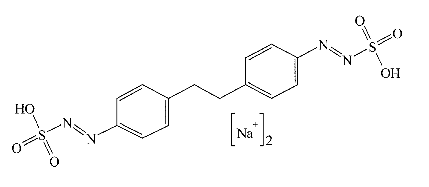

- Material nach Anspruch 1, dadurch gekennzeichnet, dass die lichtempfindliche Komponente, die bei Belichtung die Entfernbarkeit der belichteten Bereiche der Außenschicht im Vergleich zur Entfernbarkeit der unbelichteten Bereiche der Außenschicht zu ändern vermag, ein Polymer oder Copolymer eines Aryldiazosulfonats ist, das die Entfernbarkeit der belichteten Bereiche der Außenschicht verringert.
- Material nach Anspruch 1, dadurch gekennzeichnet, dass die lichtempfindliche Komponente, die bei Belichtung die Entfernbarkeit der belichteten Bereiche der Außenschicht im Vergleich zur Entfernbarkeit der unbelichteten Bereiche der Außenschicht zu ändern vermag, eine Chinondiazidverbindung ist, welche die Entfernbarkeit der belichteten Bereiche der Außenschicht steigert.
- Ein Verfahren zur Herstellung eines elektrisch leitfähigen Musters auf einem Träger, wobei das Verfahren folgende Schritte umfasst :- Bereitstellen eines Materials zur Herstellung eines elektrisch leitfähigen Musters, wobei das Material einen Träger und ein bei Belichtung differenzierbares Element umfasst, wobei das bei Belichtung differenzierbare Element eine Außenschicht, die ein Polyanion und ein Polymer oder Copolymer eines gegebenenfalls substituierten Thiophens enthält, und gegebenenfalls eine an die Außenschicht grenzende zweite Schicht umfasst und wobei die Außenschicht und/oder die eventuelle zweite Schicht eine lichtempfindliche Komponente enthält, die bei Belichtung die Entfernbarkeit der belichteten Bereiche der Außenschicht im Vergleich zur Entfernbarkeit der unbelichteten Bereiche der Außenschicht zu ändern vermag, dadurch gekennzeichnet, dass die lichtempfindliche Komponente ein Multidiazoniumsalz, ein diazoniumsalzhaltiges Harz oder eine Chinondiazidverbindung ist,- bildmäßige Belichtung des Materials, wobei gegebenenfalls unter Verwendung eines Entwicklers eine Differenzierung der Entfernbarkeit zwischen den belichteten Bereichen und den unbelichteten Bereichen der Außenschicht hervorgerufen wird,- Entwicklung des Materials, gegebenenfalls unter Verwendung des Entwicklers, wobei Bereiche der Außenschicht entfernt werden, und- gegebenenfalls die Verarbeitung des Materials zur Steigerung der elektrischen Leitfähigkeit der nicht-entfernten Bereiche der Außenschicht.
- Verfahren nach Anspruch 10, dadurch gekennzeichnet, dass das Polymer eines gegebenenfalls substituierten Thiophens wasserdispergierbar ist.
- Verfahren nach Anspruch 10, dadurch gekennzeichnet, dass das Polymer eines gegebenenfalls substituierten Thiophens folgender Formel (II) entspricht :

- Verfahren nach Anspruch 10, dadurch gekennzeichnet, dass die nicht-entfernten Bereiche der Außenschicht einen Oberflächenwiderstand von weniger als 106 Ω/Quadrat aufweisen.
- Ein keinen Entfernungsschritt umfassendes Verfahren zur Herstellung eines elektrisch leitfähigen Musters auf einem Träger, wobei das Verfahren folgende Schritte umfasst :- Bereitstellen eines Materials zur Herstellung eines elektrisch leitfähigen Musters, wobei das Material einen Träger und ein bei Belichtung differenzierbares Element umfasst, dadurch gekennzeichnet, dass das bei Belichtung differenzierbare Element eine Außenschicht, die ein Polyanion und ein Polymer oder Copolymer eines gegebenenfalls substituierten Thiophens mit einem Oberflächenwiderstand von weniger als 106 Ω/Quadrat enthält, und gegebenenfalls eine an die Außenschicht grenzende zweite Schicht umfasst und wobei die Außenschicht und/oder die eventuelle zweite Schicht ein Aryldiazosulfonat gemäß folgender Formel (I) enthält :
MO3S-N=N-Ar-L-Ar-N=N-SO3M (I)
wobei Ar eine gegebenenfalls substituierte Arylgruppe, L eine zweiwertige Verbindungsgruppe und M ein Kation bedeutet, wobei das Aryldiazosulfonat der Formel (I) die Entfernbarkeit der belichteten Bereiche der Außenschicht im Vergleich zur Entfernbarkeit der unbelichteten Bereiche der Außenschicht zu ändern vermag, und- bildmäßige Belichtung des Materials, wobei gegebenenfalls unter Verwendung eines Entwicklers eine Verringerung der Leitfähigkeit der belichteten Bereiche im Vergleich zu den unbelichteten Bereichen hervorgerufen wird. - Keinen Entfernungsschritt umfassendes Verfahren zur Herstellung eines elektrisch leitfähigen Musters auf einem Träger nach Anspruch 14, dadurch gekennzeichnet, dass die Bis(aryldiazosulfonat)-Verbindung der Formel (I) aus folgender Gruppe gewählt wird :


Priority Applications (1)
| Application Number | Priority Date | Filing Date | Title |
|---|---|---|---|
| EP01978242A EP1297385B1 (de) | 2000-06-26 | 2001-06-22 | Material und verfahren für die herstellung eines elektrisch leitfähigen musters |
Applications Claiming Priority (4)
| Application Number | Priority Date | Filing Date | Title |
|---|---|---|---|
| EP00202216 | 2000-06-26 | ||
| EP00202216 | 2000-06-26 | ||
| PCT/EP2001/007083 WO2002006898A2 (en) | 2000-06-26 | 2001-06-22 | Material and method for making an electroconductive pattern |
| EP01978242A EP1297385B1 (de) | 2000-06-26 | 2001-06-22 | Material und verfahren für die herstellung eines elektrisch leitfähigen musters |
Publications (2)
| Publication Number | Publication Date |
|---|---|
| EP1297385A2 EP1297385A2 (de) | 2003-04-02 |
| EP1297385B1 true EP1297385B1 (de) | 2008-06-04 |
Family
ID=8171695
Family Applications (1)
| Application Number | Title | Priority Date | Filing Date |
|---|---|---|---|
| EP01978242A Expired - Lifetime EP1297385B1 (de) | 2000-06-26 | 2001-06-22 | Material und verfahren für die herstellung eines elektrisch leitfähigen musters |
Country Status (7)
| Country | Link |
|---|---|
| EP (1) | EP1297385B1 (de) |
| JP (1) | JP2004504693A (de) |
| KR (1) | KR20030076241A (de) |
| CN (1) | CN100335970C (de) |
| AU (1) | AU2002210414A1 (de) |
| DE (1) | DE60134317D1 (de) |
| WO (1) | WO2002006898A2 (de) |
Families Citing this family (17)
| Publication number | Priority date | Publication date | Assignee | Title |
|---|---|---|---|---|
| JP4294489B2 (ja) | 2002-02-05 | 2009-07-15 | コーニンクレッカ フィリップス エレクトロニクス エヌ ヴィ | 感光性組成物 |
| JP4344589B2 (ja) * | 2003-11-11 | 2009-10-14 | 富士通株式会社 | 導電性樹脂組成物、導電性樹脂膜、電子装置の製造方法 |
| US20080007518A1 (en) * | 2006-06-23 | 2008-01-10 | Debasis Majumdar | Conductive polymer coating with improved aging stability |
| EP2057699B1 (de) | 2006-08-21 | 2018-10-17 | Agfa-Gevaert | Uv-fotopolymerisierbare zusammensetzung zur herstellung organischer leitfähiger schichten oder strukturen |
| CN101681131A (zh) * | 2007-06-12 | 2010-03-24 | 东亚合成株式会社 | 导电性高分子上的抗蚀剂膜的剥离剂、抗蚀剂膜的剥离方法及具有已图案化的导电性高分子的基板 |
| WO2010013642A1 (ja) * | 2008-07-29 | 2010-02-04 | 東亞合成株式会社 | 導電性高分子のパターン形成方法 |
| WO2011055663A1 (ja) * | 2009-11-04 | 2011-05-12 | コニカミノルタホールディングス株式会社 | 透明電極および有機電子デバイス |
| WO2011077804A1 (ja) * | 2009-12-22 | 2011-06-30 | コニカミノルタホールディングス株式会社 | 透明電極および有機電子デバイス |
| WO2011105148A1 (ja) * | 2010-02-24 | 2011-09-01 | コニカミノルタホールディングス株式会社 | 透明導電膜、および有機エレクトロルミネッセンス素子 |
| US9306186B2 (en) | 2010-03-17 | 2016-04-05 | Konica Minolta, Inc. | Organic electronic device and method of manufacturing the same |
| WO2011125537A1 (ja) * | 2010-04-05 | 2011-10-13 | コニカミノルタホールディングス株式会社 | 透明電極及びそれを用いた有機電子素子 |
| JP5720680B2 (ja) * | 2010-05-28 | 2015-05-20 | コニカミノルタ株式会社 | 有機電子デバイス用電極 |
| WO2012005116A1 (ja) * | 2010-07-06 | 2012-01-12 | コニカミノルタホールディングス株式会社 | 有機光電変換素子およびその製造方法 |
| WO2012014621A1 (ja) * | 2010-07-29 | 2012-02-02 | コニカミノルタホールディングス株式会社 | 透明導電膜、および有機エレクトロルミネッセンス素子 |
| WO2012039240A1 (ja) * | 2010-09-24 | 2012-03-29 | コニカミノルタホールディングス株式会社 | 透明電極の製造方法及び有機電子デバイス |
| JP5880444B2 (ja) * | 2010-12-13 | 2016-03-09 | コニカミノルタ株式会社 | 透明面電極、有機エレクトロニクス素子及び透明面電極の製造方法 |
| DE102020130905A1 (de) | 2020-02-26 | 2021-08-26 | Taiwan Semiconductor Manufacturing Co., Ltd. | Strukturieren von Interconnects und anderer Aufbauten durch Photosensibilisierungsverfahren |
Family Cites Families (8)
| Publication number | Priority date | Publication date | Assignee | Title |
|---|---|---|---|---|
| CH640354A5 (fr) * | 1981-03-24 | 1983-12-30 | Seitz Sa | Centreur pour connecteur de fibres optiques. |
| US4914039A (en) * | 1988-04-20 | 1990-04-03 | Hoechst Celanese Corporation | Water developable, negative working overlay or transfer type diazo color proofing system |
| DE3903421A1 (de) * | 1989-02-06 | 1990-08-09 | Hoechst Ag | Elektrisch leitfaehige resistmasse, verfahren zu ihrer herstellung und ihre verwendung |
| US5246818A (en) * | 1989-08-16 | 1993-09-21 | Hoechst Celanese Corporation | Developer composition for positive working color proofing films |
| US5561030A (en) * | 1991-05-30 | 1996-10-01 | Simon Fraser University | Fabrication of electronically conducting polymeric patterns |
| JPH05226238A (ja) * | 1991-10-31 | 1993-09-03 | Internatl Business Mach Corp <Ibm> | E−ビームレジスト用の塩基現像可能な放電トップ層 |
| JP3112745B2 (ja) * | 1992-06-17 | 2000-11-27 | 富士通株式会社 | パターン形成用導電性組成物及び該組成物を用いたパターン形成方法 |
| US5370825A (en) * | 1993-03-03 | 1994-12-06 | International Business Machines Corporation | Water-soluble electrically conducting polymers, their synthesis and use |
-
2001
- 2001-06-22 JP JP2002512745A patent/JP2004504693A/ja not_active Withdrawn
- 2001-06-22 EP EP01978242A patent/EP1297385B1/de not_active Expired - Lifetime
- 2001-06-22 WO PCT/EP2001/007083 patent/WO2002006898A2/en not_active Ceased
- 2001-06-22 KR KR1020027017658A patent/KR20030076241A/ko not_active Withdrawn
- 2001-06-22 AU AU2002210414A patent/AU2002210414A1/en not_active Abandoned
- 2001-06-22 CN CNB018118364A patent/CN100335970C/zh not_active Expired - Fee Related
- 2001-06-22 DE DE60134317T patent/DE60134317D1/de not_active Expired - Fee Related
Also Published As
| Publication number | Publication date |
|---|---|
| WO2002006898A3 (en) | 2002-05-02 |
| WO2002006898A2 (en) | 2002-01-24 |
| JP2004504693A (ja) | 2004-02-12 |
| EP1297385A2 (de) | 2003-04-02 |
| CN100335970C (zh) | 2007-09-05 |
| AU2002210414A1 (en) | 2002-01-30 |
| DE60134317D1 (de) | 2008-07-17 |
| KR20030076241A (ko) | 2003-09-26 |
| CN1439117A (zh) | 2003-08-27 |
Similar Documents
| Publication | Publication Date | Title |
|---|---|---|
| Angelopoulos | Conducting polymers in microelectronics | |
| US6638680B2 (en) | Material and method for making an electroconductive pattern | |
| US6685853B1 (en) | Energy sensitive electrically conductive admixtures, uses thereof, methods of fabrication and structures fabricated therewith | |
| WO2002006898A2 (en) | Material and method for making an electroconductive pattern | |
| US6746751B2 (en) | Material having a conductive pattern and a material and method for making a conductive pattern | |
| US6649327B2 (en) | Method of patterning electrically conductive polymers | |
| EP0540448A1 (de) | In Base entwickelbarer Entladungsüberzug für Elektronenstrahlresists | |
| EP1402319B1 (de) | Material mit leitfähigem muster und material sowie methode zur herstellung eines leitfähigen musters | |
| US6623903B2 (en) | Material and method for making an electroconductive pattern | |
| KR100418739B1 (ko) | 조절된피에이치를갖는전기전도성중합체를포함하는조성물,상기전기전도성중합체의층을포함하는레지스트구조물,이구조물의제조방법 | |
| US20110165389A1 (en) | Method for forming conductive polymer pattern | |
| JP4077405B2 (ja) | 導電性パターンの形成のための材料及び方法 | |
| EP0348961B1 (de) | Verfahren und Vorrichtung zur Herstellung von Feinstrukturen | |
| KR100948496B1 (ko) | 기능성 박막의 형성방법 | |
| TW554249B (en) | Material and method for making an electroconductive pattern |
Legal Events
| Date | Code | Title | Description |
|---|---|---|---|
| PUAI | Public reference made under article 153(3) epc to a published international application that has entered the european phase |
Free format text: ORIGINAL CODE: 0009012 |
|
| 17P | Request for examination filed |
Effective date: 20030127 |
|
| AK | Designated contracting states |
Kind code of ref document: A2 Designated state(s): AT BE CH CY DE DK ES FI FR GB GR IE IT LI LU MC NL PT SE TR |
|
| AX | Request for extension of the european patent |
Extension state: AL LT LV MK RO SI |
|
| 17Q | First examination report despatched |
Effective date: 20031007 |
|
| RBV | Designated contracting states (corrected) |
Designated state(s): DE FR GB |
|
| GRAP | Despatch of communication of intention to grant a patent |
Free format text: ORIGINAL CODE: EPIDOSNIGR1 |
|
| GRAS | Grant fee paid |
Free format text: ORIGINAL CODE: EPIDOSNIGR3 |
|
| GRAA | (expected) grant |
Free format text: ORIGINAL CODE: 0009210 |
|
| AK | Designated contracting states |
Kind code of ref document: B1 Designated state(s): DE FR GB |
|
| REG | Reference to a national code |
Ref country code: GB Ref legal event code: FG4D |
|
| REF | Corresponds to: |
Ref document number: 60134317 Country of ref document: DE Date of ref document: 20080717 Kind code of ref document: P |
|
| PLBE | No opposition filed within time limit |
Free format text: ORIGINAL CODE: 0009261 |
|
| STAA | Information on the status of an ep patent application or granted ep patent |
Free format text: STATUS: NO OPPOSITION FILED WITHIN TIME LIMIT |
|
| 26N | No opposition filed |
Effective date: 20090305 |
|
| PGFP | Annual fee paid to national office [announced via postgrant information from national office to epo] |
Ref country code: FR Payment date: 20090617 Year of fee payment: 9 |
|
| PGFP | Annual fee paid to national office [announced via postgrant information from national office to epo] |
Ref country code: DE Payment date: 20090613 Year of fee payment: 9 Ref country code: GB Payment date: 20090619 Year of fee payment: 9 |
|
| GBPC | Gb: european patent ceased through non-payment of renewal fee |
Effective date: 20100622 |
|
| REG | Reference to a national code |
Ref country code: FR Ref legal event code: ST Effective date: 20110228 |
|
| PG25 | Lapsed in a contracting state [announced via postgrant information from national office to epo] |
Ref country code: DE Free format text: LAPSE BECAUSE OF NON-PAYMENT OF DUE FEES Effective date: 20110101 |
|
| PG25 | Lapsed in a contracting state [announced via postgrant information from national office to epo] |
Ref country code: FR Free format text: LAPSE BECAUSE OF NON-PAYMENT OF DUE FEES Effective date: 20100630 |
|
| PG25 | Lapsed in a contracting state [announced via postgrant information from national office to epo] |
Ref country code: GB Free format text: LAPSE BECAUSE OF NON-PAYMENT OF DUE FEES Effective date: 20100622 |