EP1297672B1 - Entscheidungsgeführter trägerfrequenzdetektor und verfahren für qam - Google Patents
Entscheidungsgeführter trägerfrequenzdetektor und verfahren für qam Download PDFInfo
- Publication number
- EP1297672B1 EP1297672B1 EP00943368A EP00943368A EP1297672B1 EP 1297672 B1 EP1297672 B1 EP 1297672B1 EP 00943368 A EP00943368 A EP 00943368A EP 00943368 A EP00943368 A EP 00943368A EP 1297672 B1 EP1297672 B1 EP 1297672B1
- Authority
- EP
- European Patent Office
- Prior art keywords
- signal
- qam
- frequency
- carrier signal
- rotation
- Prior art date
- Legal status (The legal status is an assumption and is not a legal conclusion. Google has not performed a legal analysis and makes no representation as to the accuracy of the status listed.)
- Expired - Lifetime
Links
- 238000000034 method Methods 0.000 title claims abstract description 14
- 238000005070 sampling Methods 0.000 claims abstract description 7
- 230000001360 synchronised effect Effects 0.000 claims description 9
- 238000004891 communication Methods 0.000 claims description 8
- 230000005540 biological transmission Effects 0.000 claims description 3
- 238000001914 filtration Methods 0.000 claims 1
- 241001417527 Pempheridae Species 0.000 description 8
- 238000010586 diagram Methods 0.000 description 4
- 238000011084 recovery Methods 0.000 description 4
- 238000012883 sequential measurement Methods 0.000 description 2
- 230000007704 transition Effects 0.000 description 2
- MCCYTOKKEWJAMY-UHFFFAOYSA-N 4-amino-n-(4-methoxy-1,2,5-thiadiazol-3-yl)benzenesulfonamide;5-[(3,4,5-trimethoxyphenyl)methyl]pyrimidine-2,4-diamine Chemical group COC1=NSN=C1NS(=O)(=O)C1=CC=C(N)C=C1.COC1=C(OC)C(OC)=CC(CC=2C(=NC(N)=NC=2)N)=C1 MCCYTOKKEWJAMY-UHFFFAOYSA-N 0.000 description 1
- 238000012937 correction Methods 0.000 description 1
- 238000013461 design Methods 0.000 description 1
Images

Classifications
-
- H—ELECTRICITY
- H04—ELECTRIC COMMUNICATION TECHNIQUE
- H04L—TRANSMISSION OF DIGITAL INFORMATION, e.g. TELEGRAPHIC COMMUNICATION
- H04L27/00—Modulated-carrier systems
- H04L27/32—Carrier systems characterised by combinations of two or more of the types covered by groups H04L27/02, H04L27/10, H04L27/18 or H04L27/26
- H04L27/34—Amplitude- and phase-modulated carrier systems, e.g. quadrature-amplitude modulated carrier systems
- H04L27/38—Demodulator circuits; Receiver circuits
- H04L27/3818—Demodulator circuits; Receiver circuits using coherent demodulation, i.e. using one or more nominally phase synchronous carriers
- H04L27/3827—Demodulator circuits; Receiver circuits using coherent demodulation, i.e. using one or more nominally phase synchronous carriers in which the carrier is recovered using only the demodulated baseband signals
-
- H—ELECTRICITY
- H04—ELECTRIC COMMUNICATION TECHNIQUE
- H04L—TRANSMISSION OF DIGITAL INFORMATION, e.g. TELEGRAPHIC COMMUNICATION
- H04L27/00—Modulated-carrier systems
- H04L27/0014—Carrier regulation
- H04L2027/0024—Carrier regulation at the receiver end
- H04L2027/0026—Correction of carrier offset
- H04L2027/0028—Correction of carrier offset at passband only
-
- H—ELECTRICITY
- H04—ELECTRIC COMMUNICATION TECHNIQUE
- H04L—TRANSMISSION OF DIGITAL INFORMATION, e.g. TELEGRAPHIC COMMUNICATION
- H04L27/00—Modulated-carrier systems
- H04L27/0014—Carrier regulation
- H04L2027/0044—Control loops for carrier regulation
- H04L2027/0053—Closed loops
- H04L2027/0057—Closed loops quadrature phase
-
- H—ELECTRICITY
- H04—ELECTRIC COMMUNICATION TECHNIQUE
- H04L—TRANSMISSION OF DIGITAL INFORMATION, e.g. TELEGRAPHIC COMMUNICATION
- H04L27/00—Modulated-carrier systems
- H04L27/0014—Carrier regulation
- H04L2027/0044—Control loops for carrier regulation
- H04L2027/0063—Elements of loops
- H04L2027/0065—Frequency error detectors
-
- H—ELECTRICITY
- H04—ELECTRIC COMMUNICATION TECHNIQUE
- H04L—TRANSMISSION OF DIGITAL INFORMATION, e.g. TELEGRAPHIC COMMUNICATION
- H04L27/00—Modulated-carrier systems
- H04L27/0014—Carrier regulation
- H04L2027/0044—Control loops for carrier regulation
- H04L2027/0063—Elements of loops
- H04L2027/0067—Phase error detectors
Definitions
- the present invention relates to a communication system that performs digital data transmission using quadrature amplitude modulation (QAM).
- QAM quadrature amplitude modulation
- the QAM signal is received at a receiving unit and demodulated in order to obtain the digital data.
- the demodulator typically includes a carrier signal that is synchronized with the QAM signal.
- the carrier signal is typically generated by a voltage controlled oscillator (VCO).
- VCO voltage controlled oscillator
- the carrier signal is used to quadrature-demodulate the signal and generate baseband signals.
- the baseband signals typically comprise an I-phase signal and a Q-phase signal.
- the I-phase and Q-phase signals are amplified and converted to digital output signals that may be plotted in a phase plane with predetermined coordinates. For example, in a 64-QAM there are 64 lattice points, 8 points horizontally and 8 points vertically.
- the amplitude of the I-phase baseband signal is plotted along the horizontal axis and the amplitude of the Q-phase baseband signal is plotted along the vertical axis.
- a phase comparator generates an error signal based on the phase error between the baseband signals.
- the error signal is filtered and applied as a control signal to the VCO.
- the frequency of the carrier signal generated by the VCO is adjusted in order to rotate the baseband signals into coincidence with the predetermined lattice points in the phase plane.
- Previous systems typically used a sweeper to establish synchronization between the signals.
- the sweeper was activated when an out-of-synchronization condition was detected and caused the frequency of the VCO to slowly "sweep" over a predetermined capture range until the phases were matched. Once the phases were synchronized the sweeper was stopped and normal operation of the system was resumed. The time required to reestablish synchronization depended on the sweeper speed. A sweeper operating with a cycle of between several hundred milliseconds to several seconds could take up to several seconds to reestablish synchronization.
- U.S. Patent No. 5,594,389 discloses an area judging device for providing a signal that indicates whether the baseband signal lies inside a predetermined area in the phase plane. Just before the baseband signal rotates out of the designated area a control signal is generated to force the baseband signal in the opposite direction of rotation. It discloses holding circuits for maintaining the control signal constant until the baseband signal returns to the designated area by such counter-rotation.
- the area system is complex and more difficult to implement than the sweeper system and there remains a need for a simple decision directed system that is capable of quickly restoring synchronization between the carrier signal and the QUAM signal.
- US Patent No. 4,308,505 describes a frequency detector and method for use in timing and carrier recovery applications in which the direction of rotation of the baseband signal is determined by sequential sampling of the baseband signal relative to quadrants of the phase plane.
- the direction of rotation is derived by determining if successive samples within a predetermined region cross the axis of the phase plane. Upon a crossing of the axis, signals are generated to increase or decrease the frequency of the baseband VCO.
- the specification thus discloses determining the direction of rotation by the baseband signal's procession across the axis of the phase plane and not based on changes relative to predetermined points as described in the claims of the present application.
- JP- 61059949 abstract discloses controlling the carrier VCO in response to a shift from a predetermined reference point. The relative change in successive samples is not measured, only the value of the shift from the predetermined point. There is no disclosure determining the direction of rotation of the baseband signal through sequential measurements of the baseband signal relative to predetermined points as in the present application.
- the area system is complex and more difficult to implement than the sweeper system and there remains a need for a simple decision directed system that is capable of quickly restoring synchronization between the carrier signal and the QAM signal.
- the present invention includes a communication system that performs data transmission using a quadrature amplitude modulated (QAM) signal comprising a controlled oscillator (VCO) for generating a carrier signal, a frequency detector characterized by means for determining a direction of rotation of a baseband signal in a phase plane, the baseband signal is the QAM signal demodulated with the carrier signal, and means for generating a control signal for said controlled oscillator to change a frequency of the carrier signal to match a frequency of the QAM signal, wherein said means for determining the direction of rotation of the baseband signal includes means for obtaining a phase difference from two samples of the baseband signal obtained at two consecutive points in time based on sample locations in different QAM symbol quadrants within a quadrant of the phase plane, wherein for each QAM symbol associated with the QAM signal its associated QAM symbol quadrants are located adjacent to and in opposing regions of the QAM symbol.
- QAM quadrature amplitude modulated
- VCO controlled oscillator
- the invention also includes a decision directed carrier frequency detector for a demodulator carrier signal comprising means for sampling a baseband signal at consecutive points in time, means for determining a difference in phase from the two sample points, based on sample locations in different quadrature amplitude modulation (QAM) symbol quadrants within a quadrant of a phase plane, wherein for each QAM symbol its associated QAM symbol quadrants are located adjacent to and in opposing regions of the QAM symbol, and means for disabling the frequency detector when the carrier signal and a QAM signal associated with the QAM symbol are synchronized.
- QAM quadrature amplitude modulation
- the invention furthermore includes a method for facilitating the retrieval of data from a quadrature amplitude modulated (QAM) signal comprising the steps of generating a carrier signal, providing the generated carrier signal to a demodulator, characterized by demodulating the QAM signal to provide a baseband signal comprising a constellation of QAM symbols, determining if there is rotation of the constellation and, if so, a direction of said rotation, adjusting a frequency of the carrier signal to reduce any determined rotation of the constellation, so as to synchronize the QAM signal with the carrier signal to facilitate the retrieval of data, and in which said step of adjusting the frequency of the carrier signal comprises controlling the voltage of a controlled oscillator, wherein said step of determining the direction of rotation includes sampling the baseband signal at two consecutive points in time and further includes the step of calculating a phase difference from the two samples of the baseband signal based on sample locations in different QAM symbol quadrants within a quadrant of a phase plane, wherein for each QAM symbol associated with the QAM signal its
- An object of the present invention is to provide a QAM communication system and method with a demodulator that can quickly resynchronize the carrier signal with the data carrying QAM signal, and to provide a QAM demodulator and method that includes a decision-directed carrier frequency detector for a voltage controlled oscillator.
- Another object is to provide a QAM demodulator and method that includes a decision-directed carrier frequency detector for a numerically controlled oscillator, and to provide a alternative to a VCO frequency sweeper system and method.
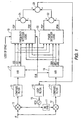
- Figure 1 shows the incoming QAM signal provided to suitable conventional mixers 10 and 12.
- the mixers 10 and 12 and 90 degree hybrid mixer 11 form a standard QAM demodulator.
- the demodulator produces output signals I and Q from the carrier signal which are applied respectively to the conventional low pass filters 13 and 14 to remove noise from the signals.
- the filtered signals are next applied respectively to analog to digital (A/ D) converters 17 and 18.
- the output signals from the A/D converters are provided to the frequency detector 19 logic circuit and the phase detector logic circuit 20. Each of the detectors may have differential output signals.
- the frequency detector 19 produce two digital output signals: Frequency Difference Positive (FDP) and Frequency Difference Negative (FDN).
- the phase detector 20 include a decision directed circuit and produces digital output signals for Phase Difference Positive (PDP) and Phase Difference Negative (FDN).
- the differential output signals from the frequency detector 19 and the phase detector 20 are applied to conventional subtractors 21 and 22 respectively.
- Each of the subtractors provides a signal with three possible values (+, - or 0).
- the output signals from the two subtractors are added by a conventional adder 23 and provided to loop filter 16.
- the filtered signal is provided to the VCO 15 to adjust the carrier signal frequency into synchronization with the frequency of the received IF signal.
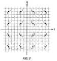
- the baseband signals produced by the A/D converters 17 and 18 of Figure 1 may be plotted in a phase plane.
- Fig. 2 illustrates a 16 QAM constellation plotted in a two dimensional phase plane. Similar constellations can be obtained for other QAM modulation schemes, for example, a plot of a 32 QAM signal will have 32 points in its constellation. A point of the constellation may be referred to by a symbol that has as its coordinates (x,y) the amplitude of the I and Q phase signals respectively.
- the VCO 15 When the demodulator is out of synchronization, the VCO 15 is not generating a carrier signal at a frequency equal to the frequency of the incoming IF signal.
- the frequency detector logic circuit 19 will detect the direction that the VCO 15 has to be steered (increase or decrease frequency), and that correction is applied to the VCO 15.
- the demodulator is synchronized (i.e. the frequency of the carrier signal and the IF signal are matched) the "Loss of Synch" signal is used to disable the frequency detector logic circuit 19. In this case, the FDP and FDN are both equal to 0.
- Each symbol of the constellation is surrounded by four quadrants, two of which may be designated A and B as shown in Fig. 2 .
- the frequency detector 19 can detect whether a symbol is in the A or B region.
- the direction of constellation rotation is detected by determining the location of a constellation point at sequential times.
- the baseband signal is sampled at two consecutive points in time, and two symbols are obtained. If a particular symbol is in the A region (as shown in Fig. 2 ) and the previous symbol was in the B region, it can be determined that the baseband constellation is rotating clockwise and that the frequency of the carrier signal is too low.
- a control signal is then generated to control the VCO 15, and raise the frequency of the carrier signal.
- the E1, E0 and M bits are obtained.
- the error bits E1 and E0 for the I and Q baseband signals are: bits numbered 3 and 4 for a 4-QAM signal; bits numbered 4 and 5 for 16-QAM; bits numbered 5 and 6 for a 32 or 64 QAM; and bits numbered 6 and 7 for a 128 or 256 QAM.
- the M bit is numbered 2 for all modulation patterns.
- FDN When the logic circuit 19 detects a transition from the A to B region, FDN is high and the loop filter 16 output signal and the frequency produced by the VCO 15 both decrease. Similarly, when the logic circuit 19 detects a transition from the B to A regions, FDP is high and the loop filter 16 output signal and the frequency of the VCO 15 both increase. In any other case, both FDP or FDN are low.
- FIG 3 illustrates the frequency detector logic circuit 19 disclosed in Figure 1 .
- the circuit 19 includes two groups of logic elements 31 and 32. Both groups comprise several AND gates and a MUX gate.
- the logic elements in group 31 detect the location of a constellation point, and produce an output signal equal to 1 if the point is inside the B region.
- the logic elements in group 32 detect the location of a constellation point, and produce an output signal equal to 1 if the point is in the A region.
- the logic circuit 19 also includes conventional flip-flops 33 and 34.
- Flip-flop 33 stores the previous state of the output signal for the group 31 elements
- flip-flop 34 stores the previous state of the output signal for the group 32 elements.
- the logic circuit also includes AND gates 35, 36, 37, and 38.
- the circuit operates so that when the present constellation point is in the A region, and the previous constellation point was in the B region, the output signals of group 32 and flip-flop 33 will be high. As a result, the output signal of gate 35 will be in a high state as will the output signal (FDP) of gate 37.
- the detector circuit also includes a "Loss of Synch” signal.
- the “Loss of Synch” signal is used to disable the frequency detector 19.
- the “Loss of Synch” signal must be high for the frequency detector 19 to operate.
- the demodulator is synchronized, the "Loss of Synch” signal is in a low state and both output signals FDP and FDN are in a low state.
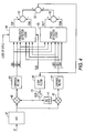
- the demodulator of the present invention may be digitally implemented.
- the system of Fig. 4 includes an A/D converter 47 that converts the incoming IF signal to a digital signal which is demodulated in mixers 40, 42 and 90 degree hybrid 41 mixer using a carrier signal produced by a numerically controlled oscillator (NCO) 45.
- NCO numerically controlled oscillator
- the mixers 40, 41 and 42 produce output signals I and Q.
- the output signals are passed through lowpass filters 43 and 44 to remove noise from the signals and are applied respectively to the frequency and phase detectors 49 and 50.
- the mixers, filters and detectors may be the same as those disclosed in Fig.1 .
- the frequency detector 49 produces digital output signals FDP and FDN and the phase detector 50 produces digital output signals PDP and PDN.
- the differential output signals from the frequency detector 49 and the phase detector 50 are applied to subtractors 51 and 52 respectively.
- Each subtractor provides a signal with three possible values +, - or 0.
- the output signals from the two subtractors are provided to the adder circuit 53 and the output signal from adder 53 is provided to a loop filter 46.
- the filtered signal is provided to the NCO 45 to synchronize the carrier signal frequency with of the received QAM signal.
- the NCO 45 functions similarly to VCO 15 described above.
- the demodulator When the demodulator is out of synchronization, the NCO 45 does not operate at a frequency equal to the carrier frequency of the incoming IF signal.
- the frequency detector logic circuit 49 detects the direction in which the NCO 45 must be steered to match the IF signal frequency. A corrective signal is then applied to the NCO 45.
- the "Loss of Synch" signal is low and the frequency detector logic circuit 49 is disabled (i.e. FDP and FDN are equal to 0).
- a decision directed frequency detector and method for a quadrature amplitude modulated signal (QAM) demodulator interacts with a voltage controlled oscillator (VCO) that generates a carrier signal to demodulate the QAM signal into a baseband signal.
- VCO voltage controlled oscillator
- the frequency detector determines the direction of rotation of the baseband signal by sampling the baseband signal relative to predetermined points in the phase plane. For example, if one sample has a negative phase offset with respect to a predetermined point and the next one has a positive phase offset, it detects that the rotation is clockwise, and vice-versa.
Landscapes
- Engineering & Computer Science (AREA)
- Computer Networks & Wireless Communication (AREA)
- Signal Processing (AREA)
- Digital Transmission Methods That Use Modulated Carrier Waves (AREA)
- Color Television Systems (AREA)
- Transmitters (AREA)
Claims (23)
- Kommunikationssystem, das eine Datenübertragung unter Verwendung eines Quadraturamplituden-modulierten (QAM) Signals durchführt und das folgende Merkmale aufweist:einen gesteuerten Oszillator (VCO) zum Erzeugen eines Trägersignals,einen Frequenzdetektor (19, 49), gekennzeichnet durch eine Einrichtung zum Bestimmen einer Drehrichtung eines Basisbandsignals in einer Phasenebene, wobei das Basisbandsignal das QAM-Signal ist, das mit dem Trägersignal demoduliert wird, undeine Einrichtung zum Erzeugen eines Steuersignals für den gesteuerten Oszillator (15, 45), um eine Frequenz des Trägersignals zu verändern, um mit einer Frequenz des QAM-Signals zusammenzupassen, die Verbesserung, wobei die Einrichtung zum Bestimmen der Drehrichtung des Basisbandsignals eine Einrichtung zum Erhalten einer Phasendifferenz aus aufeinander folgenden Abtastwerten des Basisbandsignals, die zu zwei aufeinander folgenden Zeitpunkten erhalten werden, basierend auf Abtastwertorten in unterschiedlichen QAM-Symbolquadranten innerhalb eines Quadranten der Phasenebene umfasst,wobei bei jedem QAM-Symbol, das dem QAM-Signal zugeordnet ist, seine zugeordneten QAM-Symbolquadranten bezüglich des QAM-Symbols benachbart und in gegenüberliegenden Regionen angeordnet sind.
- System gemäß Anspruch 1, dadurch gekennzeichnet, dass der Frequenzdetektor (19, 49) folgende Merkmale umfasst:eine Einrichtung zum Implementieren eines entscheidungsgeführten Algorithmus, um die Frequenz des Trägersignals zu erfassen, undwobei das Verändern der Frequenz des Trägersignals, um mit der Frequenz des QAM-Signals zusammenzupassen, ein Verringern der Frequenz des Trägersignals umfasst, wenn der Frequenzdetektor (19, 49) basierend auf der erhaltenen Phasendifferenz bestimmt, dass das Basisbandsignal sich gegen den Uhrzeigersinn dreht.
- System gemäß Anspruch 1, dadurch gekennzeichnet, dass der gesteuerte Oszillator (VCO) eine Einrichtung zum Erhöhen der Frequenz des Trägersignals, wenn der Frequenzdetektor (19, 49) basierend auf der erhaltenen Phasendifferenz bestimmt, dass sich das Basisbandsignal im Uhrzeigersinn dreht, umfasst.
- System gemäß Anspruch 1, gekennzeichnet durch ein Schleifenfilter zwischen dem Frequenzdetektor (19, 49) und dem gesteuerten Oszillator (15, 45) zum Herausfiltern der Hochfrequenzkomponenten des Steuersignals vor dem gesteuerten Oszillator (15, 45).
- System gemäß Anspruch 1, dadurch gekennzeichnet, dass die Einrichtung zum Bestimmen der Drehrichtung ein Frequenzdifferenz-Positiv- (FDP) Signal und ein Frequenzdifferenz-Negativ- (FDN) Signal erzeugt, und das einen Subtrahierer zwischen dem Frequenzdetektor (19, 49) und dem gesteuerten Oszillator (15, 45) umfasst, wobei der Subtrahierer als seine Eingangssignale die FDN- und FDP-Signale aufweist, und das Ausgangssignal des Subtrahierers in einem niedrigen Zustand ist, wenn das FDN-Signal in einem hohen Zustand ist, und das Ausgangssignal in einem hohen Zustand ist, wenn das FDP in einem hohen Zustand ist.
- System gemäß Anspruch 1, gekennzeichnet durch einen Phasendetektor (20, 50) zum Erfassen einer Differenz zwischen einer Phase des QAM-Signals und des Trägersignals, und
wobei die Einrichtung zum Berechnen der Phasendifferenz aus der Mehrzahl von Abtastwerten zwei Abtastpunkte verwendet. - Entscheidungsgeführter Trägerfrequenzdetektor für ein Demodulatorträgersignal, der folgende Merkmale aufweist:eine Einrichtung zum Abtasten eines Basisbandsignals zu zwei aufeinander folgenden Zeitpunkten,eine Einrichtung zum Bestimmen einer Phasendifferenz aus den beiden Abtastpunkten basierend auf Abtastwertorten in unterschiedlichen Quadraturamplitudenmodulations-(QAM) Symbolquadranten innerhalb eines Quadranten einer Phasenebene, wobei bei jedem QAM-Symbol seine zugeordneten QAM-Symbolquadranten bezüglich des QAM-Symbols benachbart und in gegenüberliegenden Regionen angeordnet sind, undeine Einrichtung zum Deaktivieren des Frequenzdetektors (19, 49), wenn das Trägersignal und ein QAM-Signal, das dem QAM-Symbol zugeordnet ist, synchronisiert sind.
- Verfahren zum Ermöglichen der Gewinnung von Daten aus einem Quadraturamplituden-modulierten (QAM) Signal, das folgende Schritte aufweist:Erzeugen eines Trägersignals,Liefern des erzeugten Trägersignals an einen Demodulator, gekennzeichnet durch ein Demodulieren des QAM-Signals, um ein Basisbandsignal zu liefern, das eine Konstellation von QAM-Symbolen aufweist,Bestimmen, ob eine Drehung der Konstellation vorliegt, und, falls dies der Fall ist, einer Richtung der Drehung,Anpassen einer Frequenz des Trägersignals, um eine beliebige bestimmte Drehung der Konstellation zu verringern, um das QAM-Signal mit dem Trägersignal zu synchronisieren, um die Gewinnung von Daten zu ermöglichen, undwobei der Schritt des Anpassens der Frequenz des Trägersignals folgenden Schritt aufweist:Steuern der Spannung eines gesteuerten Oszillators (15, 45),wobei der Schritt des Bestimmens der Drehrichtung ein Abtasten des Basisbandsignals zu zwei aufeinander folgenden Zeitpunkten umfasst und ferner den Schritt eines Berechnens einer Phasendifferenz aus den zwei Abtastwerten des Basisbandsignals basierend auf Abtastwertorten in unterschiedlichen QAM-Symbolquadranten innerhalb eines Quadranten einer Phasenebene umfasst,
wobei bei jedem QAM-Symbol, das dem QAM-Signal zugeordnet ist, seine zugeordneten QAM-Symbolquadranten bezüglich des QAM-Symbols benachbart und in gegenüberliegenden Regionen angeordnet sind,
was den Schritt eines Erzeugens eines Steuersignals für den gesteuerten Oszillator (VCO), nachdem die Drehrichtung bestimmt worden ist, umfasst. - Verfahren gemäß Anspruch 8, gekennzeichnet durch den Schritt, das Steuersignal nicht fortzusetzen, wenn das QAM-Signal und das Trägersignal synchronisiert sind.
- System gemäß Anspruch 1, dadurch gekennzeichnet, dass der Frequenzdetektor (19, 49) eine Logikschaltung umfasst.
- System gemäß Anspruch 1, gekennzeichnet durch einen Demodulator zum Erzeugen des Basisbandsignals.
- System gemäß Anspruch 1, dadurch gekennzeichnet, dass die Frequenz des Trägersignals durch ein Steuersignal gesteuert wird, das von dem gesteuerten Oszillator (15, 45) empfangen wird.
- System gemäß Anspruch 1, gekennzeichnet durch eine Einrichtung zum Erhalten der Abtastwerte des Basisbandsignals zu aufeinander folgenden Zeitpunkten.
- System gemäß Anspruch 1, gekennzeichnet durch eine Einrichtung zum Bestimmen einer Konstellationsdrehung aus der erhaltenen Phasendifferenz der Abtastwerte.
- System gemäß Anspruch 14, gekennzeichnet durch eine Einrichtung zum Anpassen des Steuersignals, so dass die bestimmte Konstellationsdrehung verringert wird.
- System gemäß Anspruch 1, dadurch gekennzeichnet, dass der gesteuerte Oszillator einen spannungsgesteuerten Oszillator (15) umfasst.
- System gemäß Anspruch 1, dadurch gekennzeichnet, dass der gesteuerte Oszillator einen numerisch gesteuerten Oszillator (45) umfasst.
- System gemäß Anspruch 1, gekennzeichnet durch eine Einrichtung zum Deaktivieren des Frequenzdetektors (19, 49), wenn das Trägersignal und das QAM-Signal synchronisiert sind.
- Frequenzdetektor gemäß Anspruch 7, dadurch gekennzeichnet, dass die Einrichtung zum Bestimmen eine Logikschaltung umfasst.
- Frequenzdetektor gemäß Anspruch 19, dadurch gekennzeichnet, dass die Logikschaltung eine Mehrzahl von Logikgattern umfasst und Frequenzdifferenz-Negativ- und Frequenzdifferenz-Positiv-Ausgangssignale erzeugt.
- Verfahren gemäß Anspruch 8, dadurch gekennzeichnet, dass der Schritt des Anpassens der Frequenz des Trägersignals ein Erhöhen der Frequenz des Trägersignals umfasst, wenn bestimmt wird, dass die Drehrichtung im Uhrzeigersinn ist.
- Verfahren gemäß Anspruch 8, dadurch gekennzeichnet, dass der Schritt des Anpassens der Frequenz des Trägersignals ein Erniedrigen der Frequenz des Trägersignals umfasst, wenn bestimmt wird, dass die Drehrichtung gegen den Uhrzeigersinn ist.
- System gemäß Anspruch 1, gekennzeichnet durch einen Demodulator zum Erzeugen des Basisbandsignals durch ein Demodulieren des QAM-Signals mit dem Trägersignal.
Applications Claiming Priority (2)
| Application Number | Priority Date | Filing Date | Title |
|---|---|---|---|
| US09/323,211 US6738429B1 (en) | 1999-06-01 | 1999-06-01 | Decision-directed carrier frequency detector and method for QAM |
| PCT/US2000/018243 WO2002003643A1 (en) | 1999-06-01 | 2000-06-30 | Decsion-directed carrier frequency detector and method for qam |
Publications (2)
| Publication Number | Publication Date |
|---|---|
| EP1297672A1 EP1297672A1 (de) | 2003-04-02 |
| EP1297672B1 true EP1297672B1 (de) | 2008-10-29 |
Family
ID=32852853
Family Applications (1)
| Application Number | Title | Priority Date | Filing Date |
|---|---|---|---|
| EP00943368A Expired - Lifetime EP1297672B1 (de) | 1999-06-01 | 2000-06-30 | Entscheidungsgeführter trägerfrequenzdetektor und verfahren für qam |
Country Status (5)
| Country | Link |
|---|---|
| US (1) | US6738429B1 (de) |
| EP (1) | EP1297672B1 (de) |
| AT (1) | ATE413051T1 (de) |
| AU (1) | AU2000257845A1 (de) |
| WO (1) | WO2002003643A1 (de) |
Families Citing this family (4)
| Publication number | Priority date | Publication date | Assignee | Title |
|---|---|---|---|---|
| DE10108110A1 (de) * | 2001-02-21 | 2002-08-29 | Philips Corp Intellectual Pty | Empfänger und Verfahren zum anfänglichen Synchronisieren eines Empfängers auf die Trägerfrequenz eines gewünschten Kanals |
| GB2377345B (en) * | 2001-07-02 | 2004-06-16 | Motorola Inc | Time synchronisation system and method |
| US8654008B2 (en) | 2010-09-29 | 2014-02-18 | Qualcomm Incorporated | Multi-stage GLONASS/GPS automatic frequency control |
| US8644782B2 (en) * | 2011-11-14 | 2014-02-04 | Apple Inc. | Agile clocking with receiver PLL management |
Family Cites Families (30)
| Publication number | Priority date | Publication date | Assignee | Title |
|---|---|---|---|---|
| US4308505A (en) * | 1979-06-13 | 1981-12-29 | Trw, Inc. | Frequency detector device and method |
| JPS6155994A (ja) | 1984-08-27 | 1986-03-20 | 信越化学工業株式会社 | 銅張りフレキシブルプリント回路用基板 |
| JPS6159949A (ja) * | 1984-08-31 | 1986-03-27 | Fujitsu Ltd | 選択制御搬送波再生方式 |
| US4682111A (en) | 1985-03-05 | 1987-07-21 | Kabushiki Kaisha Toshiba | Magnetic resonance imaging magnet |
| FR2581277A1 (fr) * | 1985-04-30 | 1986-10-31 | Labo Electronique Physique | Circuit de recuperation de l'onde porteuse de systemes de transmissions numeriques |
| CA1284361C (en) | 1986-08-29 | 1991-05-21 | Mitel Corporation | Analog phase locked loop |
| FR2621188B1 (fr) * | 1987-09-25 | 1989-12-29 | Labo Electronique Physique | Circuit de recuperation de l'onde porteuse de systemes de transmissions numeriques |
| US4916405A (en) * | 1988-10-27 | 1990-04-10 | Unisys Corp. | Smart sweep apparatus for data rate receivers |
| US5042052A (en) * | 1990-02-16 | 1991-08-20 | Harris Corporation | Carrier acquisition scheme for QAM and QPSK data |
| JP2994836B2 (ja) | 1992-01-30 | 1999-12-27 | 富士通株式会社 | 復調器のafc回路 |
| US5376894A (en) * | 1992-12-31 | 1994-12-27 | Pacific Communication Sciences, Inc. | Phase estimation and synchronization using a PSK demodulator |
| DE69406151T2 (de) | 1993-01-13 | 1998-04-02 | Koninkl Philips Electronics Nv | Einrichtung zur Synchronisierung eines lokalen Trägers, in OFDM-Systemen |
| GB2280324B (en) | 1993-07-16 | 1998-07-22 | Plessey Semiconductors Ltd | Detectors |
| JP3074103B2 (ja) * | 1993-11-16 | 2000-08-07 | 株式会社東芝 | Ofdm同期復調回路 |
| US5497400A (en) | 1993-12-06 | 1996-03-05 | Motorola, Inc. | Decision feedback demodulator with phase and frequency estimation |
| US5633898A (en) | 1993-12-22 | 1997-05-27 | Matsushita Electric Industrial Co., Ltd. | Automatic frequency control apparatus for FSK receiver and FSK receiver including the same |
| KR970000661B1 (ko) | 1993-12-29 | 1997-01-16 | 현대전자산업 주식회사 | 위상오차 검출기를 사용한 판정의거 반송파 복원회로 |
| KR0157500B1 (ko) | 1994-03-25 | 1998-11-16 | 김광호 | 자동주파수조절방법 및 그 장치 |
| US5519733A (en) * | 1994-05-05 | 1996-05-21 | General Instrument Corporation Of Delaware | Method and apparatus for recovering a qam carrier |
| JP3030598B2 (ja) * | 1994-06-24 | 2000-04-10 | アンリツ株式会社 | ジッタ検出装置 |
| US5696797A (en) | 1994-07-22 | 1997-12-09 | Motorola, Inc. | Demodulator with baseband doppler shift compensation and method |
| US5533062A (en) | 1994-10-03 | 1996-07-02 | Motorola, Inc. | Method and apparatus for carrier tracking and demodulation |
| EP0719002B1 (de) * | 1994-12-22 | 2004-12-08 | Alcatel | Prozessor für Trägerrückgewinnung |
| JP3269933B2 (ja) | 1995-03-20 | 2002-04-02 | 富士通株式会社 | キャリア再生回路 |
| EP0748093A1 (de) * | 1995-06-08 | 1996-12-11 | Laboratoires D'electronique Philips S.A.S. | Digitales Übertragungssystem mit Entscheidungsmitteln zur Auswahl der Synchronisierungsart |
| JPH09214578A (ja) * | 1996-01-30 | 1997-08-15 | Fujitsu Ltd | 搬送波再生回路 |
| US5729577A (en) * | 1996-05-21 | 1998-03-17 | Motorola, Inc. | Signal processor with improved efficiency |
| US6055286A (en) | 1997-07-01 | 2000-04-25 | Hewlett-Packard Company | Oversampling rotational frequency detector |
| US6160860A (en) * | 1998-01-28 | 2000-12-12 | Lucent Technologies Inc. | Phase-locked loop (PLL) circuit containing a frequency detector for improved frequency acquisition |
| AU1607400A (en) * | 1998-11-03 | 2000-05-22 | Broadcom Corporation | Dual mode qam/vsb receiver |
-
1999
- 1999-06-01 US US09/323,211 patent/US6738429B1/en not_active Expired - Fee Related
-
2000
- 2000-06-30 WO PCT/US2000/018243 patent/WO2002003643A1/en not_active Ceased
- 2000-06-30 AT AT00943368T patent/ATE413051T1/de not_active IP Right Cessation
- 2000-06-30 EP EP00943368A patent/EP1297672B1/de not_active Expired - Lifetime
- 2000-06-30 AU AU2000257845A patent/AU2000257845A1/en not_active Abandoned
Also Published As
| Publication number | Publication date |
|---|---|
| AU2000257845A1 (en) | 2002-01-14 |
| EP1297672A1 (de) | 2003-04-02 |
| US6738429B1 (en) | 2004-05-18 |
| WO2002003643A1 (en) | 2002-01-10 |
| ATE413051T1 (de) | 2008-11-15 |
Similar Documents
| Publication | Publication Date | Title |
|---|---|---|
| US4308505A (en) | Frequency detector device and method | |
| EP4024798A1 (de) | Satellitenlaser-breitband-demodulationsverfahren und -vorrichtung | |
| WO1997030511A1 (en) | Apparatus for generating timing signal for a digital television signal receiver | |
| EP0913963B1 (de) | Detektorschaltung zur Phasensynchronisierung und Demodulator | |
| US5001727A (en) | Carrier and data recovery and demodulation system | |
| CA2148200C (en) | Method and apparatus for recovering a qam carrier | |
| US5042052A (en) | Carrier acquisition scheme for QAM and QPSK data | |
| EP0373405B1 (de) | Automatische Frequenzregelung in Anwesenheit von Daten | |
| US5594389A (en) | Carrier regeneration circuit including area judging device | |
| US8396433B2 (en) | Radio communication apparatus and DC offset adjustment method | |
| HK1000408B (en) | Automatic frequency control in the presence of data | |
| JP2932861B2 (ja) | 位相同期検出回路 | |
| US6738429B1 (en) | Decision-directed carrier frequency detector and method for QAM | |
| WO1995019676A1 (en) | Higher order digital phase loop filter | |
| GB2299227A (en) | Demodulation devices avoiding pseudo synchronization | |
| US7835259B1 (en) | Control algorithm using hysteresis sub-states in QAM modems | |
| JP3148090B2 (ja) | Ofdm信号同期復調器 | |
| JPH11355372A (ja) | 周波数再生回路および周波数再生方法 | |
| JPH04207802A (ja) | デジタル型fm信号復調装置 | |
| WO2005060412A2 (en) | Control algorithm in qam modems | |
| JP3832735B2 (ja) | 復調回路 | |
| US7970080B1 (en) | Modes of operations in QAM modems using hysteresis sub-states | |
| JPH02222343A (ja) | Afc方式 | |
| Morelos-Zaragoza et al. | A carrier recovery technique using modulation identification | |
| JP3665285B2 (ja) | 周波数偏差検出方法および周波数偏差検出器 |
Legal Events
| Date | Code | Title | Description |
|---|---|---|---|
| PUAI | Public reference made under article 153(3) epc to a published international application that has entered the european phase |
Free format text: ORIGINAL CODE: 0009012 |
|
| 17P | Request for examination filed |
Effective date: 20030127 |
|
| AK | Designated contracting states |
Designated state(s): AT BE CH CY DE DK ES FI FR GB GR IE IT LI LU MC NL PT SE Kind code of ref document: A1 Designated state(s): AT BE CH CY DE DK ES FI FR GB GR IE IT LI LU MC NL PT SE |
|
| AX | Request for extension of the european patent |
Extension state: AL LT LV MK RO SI |
|
| 17Q | First examination report despatched |
Effective date: 20061219 |
|
| GRAP | Despatch of communication of intention to grant a patent |
Free format text: ORIGINAL CODE: EPIDOSNIGR1 |
|
| RTI1 | Title (correction) |
Free format text: DECISION-DIRECTED CARRIER FREQUENCY DETECTOR AND METHOD FOR QAM |
|
| GRAS | Grant fee paid |
Free format text: ORIGINAL CODE: EPIDOSNIGR3 |
|
| GRAA | (expected) grant |
Free format text: ORIGINAL CODE: 0009210 |
|
| AK | Designated contracting states |
Kind code of ref document: B1 Designated state(s): AT BE CH CY DE DK ES FI FR GB GR IE IT LI LU MC NL PT SE |
|
| REG | Reference to a national code |
Ref country code: GB Ref legal event code: FG4D |
|
| REG | Reference to a national code |
Ref country code: CH Ref legal event code: EP |
|
| REG | Reference to a national code |
Ref country code: IE Ref legal event code: FG4D |
|
| REF | Corresponds to: |
Ref document number: 60040694 Country of ref document: DE Date of ref document: 20081211 Kind code of ref document: P |
|
| NLV1 | Nl: lapsed or annulled due to failure to fulfill the requirements of art. 29p and 29m of the patents act | ||
| PG25 | Lapsed in a contracting state [announced via postgrant information from national office to epo] |
Ref country code: AT Free format text: LAPSE BECAUSE OF FAILURE TO SUBMIT A TRANSLATION OF THE DESCRIPTION OR TO PAY THE FEE WITHIN THE PRESCRIBED TIME-LIMIT Effective date: 20081029 Ref country code: ES Free format text: LAPSE BECAUSE OF FAILURE TO SUBMIT A TRANSLATION OF THE DESCRIPTION OR TO PAY THE FEE WITHIN THE PRESCRIBED TIME-LIMIT Effective date: 20090209 |
|
| PG25 | Lapsed in a contracting state [announced via postgrant information from national office to epo] |
Ref country code: FI Free format text: LAPSE BECAUSE OF FAILURE TO SUBMIT A TRANSLATION OF THE DESCRIPTION OR TO PAY THE FEE WITHIN THE PRESCRIBED TIME-LIMIT Effective date: 20081029 Ref country code: NL Free format text: LAPSE BECAUSE OF FAILURE TO SUBMIT A TRANSLATION OF THE DESCRIPTION OR TO PAY THE FEE WITHIN THE PRESCRIBED TIME-LIMIT Effective date: 20081029 Ref country code: PT Free format text: LAPSE BECAUSE OF FAILURE TO SUBMIT A TRANSLATION OF THE DESCRIPTION OR TO PAY THE FEE WITHIN THE PRESCRIBED TIME-LIMIT Effective date: 20090330 |
|
| PG25 | Lapsed in a contracting state [announced via postgrant information from national office to epo] |
Ref country code: DK Free format text: LAPSE BECAUSE OF FAILURE TO SUBMIT A TRANSLATION OF THE DESCRIPTION OR TO PAY THE FEE WITHIN THE PRESCRIBED TIME-LIMIT Effective date: 20081029 Ref country code: BE Free format text: LAPSE BECAUSE OF FAILURE TO SUBMIT A TRANSLATION OF THE DESCRIPTION OR TO PAY THE FEE WITHIN THE PRESCRIBED TIME-LIMIT Effective date: 20081029 |
|
| PG25 | Lapsed in a contracting state [announced via postgrant information from national office to epo] |
Ref country code: SE Free format text: LAPSE BECAUSE OF FAILURE TO SUBMIT A TRANSLATION OF THE DESCRIPTION OR TO PAY THE FEE WITHIN THE PRESCRIBED TIME-LIMIT Effective date: 20090129 Ref country code: IT Free format text: LAPSE BECAUSE OF FAILURE TO SUBMIT A TRANSLATION OF THE DESCRIPTION OR TO PAY THE FEE WITHIN THE PRESCRIBED TIME-LIMIT Effective date: 20081029 |
|
| PLBE | No opposition filed within time limit |
Free format text: ORIGINAL CODE: 0009261 |
|
| STAA | Information on the status of an ep patent application or granted ep patent |
Free format text: STATUS: NO OPPOSITION FILED WITHIN TIME LIMIT |
|
| 26N | No opposition filed |
Effective date: 20090730 |
|
| PG25 | Lapsed in a contracting state [announced via postgrant information from national office to epo] |
Ref country code: MC Free format text: LAPSE BECAUSE OF NON-PAYMENT OF DUE FEES Effective date: 20090630 |
|
| REG | Reference to a national code |
Ref country code: CH Ref legal event code: PL |
|
| REG | Reference to a national code |
Ref country code: FR Ref legal event code: ST Effective date: 20100226 |
|
| PG25 | Lapsed in a contracting state [announced via postgrant information from national office to epo] |
Ref country code: CH Free format text: LAPSE BECAUSE OF NON-PAYMENT OF DUE FEES Effective date: 20090630 Ref country code: IE Free format text: LAPSE BECAUSE OF NON-PAYMENT OF DUE FEES Effective date: 20090630 Ref country code: FR Free format text: LAPSE BECAUSE OF NON-PAYMENT OF DUE FEES Effective date: 20090630 Ref country code: LI Free format text: LAPSE BECAUSE OF NON-PAYMENT OF DUE FEES Effective date: 20090630 |
|
| PG25 | Lapsed in a contracting state [announced via postgrant information from national office to epo] |
Ref country code: DE Free format text: LAPSE BECAUSE OF NON-PAYMENT OF DUE FEES Effective date: 20100101 |
|
| PG25 | Lapsed in a contracting state [announced via postgrant information from national office to epo] |
Ref country code: GR Free format text: LAPSE BECAUSE OF FAILURE TO SUBMIT A TRANSLATION OF THE DESCRIPTION OR TO PAY THE FEE WITHIN THE PRESCRIBED TIME-LIMIT Effective date: 20090130 |
|
| PG25 | Lapsed in a contracting state [announced via postgrant information from national office to epo] |
Ref country code: LU Free format text: LAPSE BECAUSE OF NON-PAYMENT OF DUE FEES Effective date: 20090630 |
|
| PG25 | Lapsed in a contracting state [announced via postgrant information from national office to epo] |
Ref country code: CY Free format text: LAPSE BECAUSE OF FAILURE TO SUBMIT A TRANSLATION OF THE DESCRIPTION OR TO PAY THE FEE WITHIN THE PRESCRIBED TIME-LIMIT Effective date: 20081029 |
|
| PGFP | Annual fee paid to national office [announced via postgrant information from national office to epo] |
Ref country code: GB Payment date: 20140627 Year of fee payment: 15 |
|
| GBPC | Gb: european patent ceased through non-payment of renewal fee |
Effective date: 20150630 |
|
| PG25 | Lapsed in a contracting state [announced via postgrant information from national office to epo] |
Ref country code: GB Free format text: LAPSE BECAUSE OF NON-PAYMENT OF DUE FEES Effective date: 20150630 |