EP1298577A2 - Synchronisation des couleurs dans des imprimantes à laser - Google Patents
Synchronisation des couleurs dans des imprimantes à laser Download PDFInfo
- Publication number
- EP1298577A2 EP1298577A2 EP02021833A EP02021833A EP1298577A2 EP 1298577 A2 EP1298577 A2 EP 1298577A2 EP 02021833 A EP02021833 A EP 02021833A EP 02021833 A EP02021833 A EP 02021833A EP 1298577 A2 EP1298577 A2 EP 1298577A2
- Authority
- EP
- European Patent Office
- Prior art keywords
- image
- resist
- writing
- color
- image formation
- Prior art date
- Legal status (The legal status is an assumption and is not a legal conclusion. Google has not performed a legal analysis and makes no representation as to the accuracy of the status listed.)
- Withdrawn
Links
Images


Classifications
-
- H—ELECTRICITY
- H04—ELECTRIC COMMUNICATION TECHNIQUE
- H04N—PICTORIAL COMMUNICATION, e.g. TELEVISION
- H04N1/00—Scanning, transmission or reproduction of documents or the like, e.g. facsimile transmission; Details thereof
- H04N1/46—Colour picture communication systems
- H04N1/50—Picture reproducers
- H04N1/506—Reproducing the colour component signals picture-sequentially, e.g. with reproducing heads spaced apart from one another in the subscanning direction
-
- G—PHYSICS
- G06—COMPUTING OR CALCULATING; COUNTING
- G06K—GRAPHICAL DATA READING; PRESENTATION OF DATA; RECORD CARRIERS; HANDLING RECORD CARRIERS
- G06K15/00—Arrangements for producing a permanent visual presentation of the output data, e.g. computer output printers
- G06K15/02—Arrangements for producing a permanent visual presentation of the output data, e.g. computer output printers using printers
- G06K15/12—Arrangements for producing a permanent visual presentation of the output data, e.g. computer output printers using printers by photographic printing, e.g. by laser printers
- G06K15/1204—Arrangements for producing a permanent visual presentation of the output data, e.g. computer output printers using printers by photographic printing, e.g. by laser printers involving the fast moving of an optical beam in the main scanning direction
- G06K15/1219—Detection, control or error compensation of scanning velocity or position, e.g. synchronisation
Definitions
- the present invention relates to an image formation apparatus and a resist adjusting method.
- a tandem system In an electronic photographing type image formation apparatus such as a laser printer or a digital copying machine, there has been employed a system called a tandem system.
- lighting of an LD laser diode
- An image holder (a photo conductor) provided for each color is main and sub scanned with each optical beam emitted from the LD.
- a line scanning according to an optical beam is a main scanning, and a scanning according to a relative movement of an image holder to a direction crossing the main scanning line is a sub scanning.
- An image is written based on this operation.
- a scanning optical system (refer to Fig. 1A, Fig. 1B and Fig.
- asynchronous detecting sensor that detects an optical beam at the outside of a writing area at an image write starting side is generally provided.
- the synchronous detecting sensor detects a passing of an optical beam scanned in the main scanning (line) direction, and starts writing an image in the main scanning direction at a predetermined timing using a generated synchronizing signal as a reference.
- Synchronous detecting sensors disposed at two points on a scanning line detect scanning beams, and can match the beams using obtained synchronous detecting signals.
- a multi-color image formation apparatus Japanese Patent Application Laid-Open No. 2001-121739
- a synchronous detecting sensor that detects a scanning optical beam of each color is provided, and this sensor measures a time interval from the occurrence of a sensor detecting signal of a color determined in advance as a reference to the occurrence of a sensor detecting signal of other color. Based on this, a relative position of a synchronous detecting sensor is obtained for each color. When a variation occurs in the position obtained as a time interval, resist is adjusted according to the variation.
- a time interval from the occurrence of a sensor detecting signal of a color determined in advance as a reference to the occurrence of a sensor detecting signal of other color is measured, and resist is adjusted based on this variation.
- resist is adjusted based on this variation.
- the sensor of a color determined in advance as a reference is disposed at the upstream side in the scanning direction with a distortion relative to the sensors of other colors. In other words, the layout of the sensors is limited, and the degree of freedom of design is made small.
- the time interval is updated based on a value measured this time.
- An adjustment value is set for resist adjustment based on the updated value. Even when there is an error in the measurement, this is reflected straight to the setting. Therefore, there is a risk that errors are accumulated, and it is difficult to maintain adjustment precision.
- an image formation apparatus that has a writing control unit that line scans an image holder in a predetermined period with optical beams emitted from a light source of which lighting is controlled corresponding to each image data of a plurality of colors, and forms one image by superimposing written images of respective colors.
- the image formation apparatus comprises a synchronous detecting unit that detects each scanning optical beam and generates a writing reference synchronization signal, and a mark pulse generating unit that generates a mark pulse at a predetermined timing from the writing reference synchronization signal.
- the writing control unit has a time measuring unit that measures a time from a writing reference signal generated in a color determined as a reference from among a plurality of colors to a mark pulse generated in other color, and a resist adjusting unit that adjusts a resist of each of other colors based on a change in a measured time when this change has occurred.
- a resist adjusting method in an image formation apparatus that carries out writing control in order to line scan an image holder in a predetermined period common to each with optical beams emitted from a light source of which lighting is controlled corresponding to each image data of a plurality of colors, and form one image by superimposing written images of the colors.
- the resist adjusting method comprises steps of generating a writing reference synchronizing signal by detecting each scanning optical beam in an operating state, generating each mark pulse at a predetermined timing from each generated writing reference synchronizing signal, measuring a time from a writing reference signal generated in a color determined as a reference from among a plurality of colors to a mark pulse generated in other color, and adjusting a resist corresponding to a change in a measured time when this change has occurred.
- Figs. 1A and 1B are diagrams that show an image writing optical system that allocates laser beams of four colors with one polygon mirror.
- Fig. 2 is a perspective view that shows a part of the image writing optical system shown in Figs. 1A and 1B.
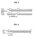
- Fig. 3 is a timing chart that shows the processing of separating DP_UA and DP_DA received by the same synchronous detector.
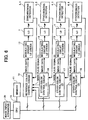
- Fig. 4 is a timing chart of a signal that shows the operation at the time of starting up a writing signal LGATE.
- Fig. 5 is a timing chart that shows a relationship of signals of other colors with a reference DP.
- Fig. 6 shows an outline structure of a circuit relating to an image write processing of an image formation apparatus according to the present invention.
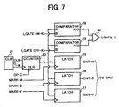
- Fig. 7 is a diagram that shows a circuit structure of a writing control circuit of a reference color shown in Fig. 6 in further detail.
- Fig. 8 is a diagram that shows a circuit structure of a writing control circuit of other colors shown in Fig. 6 in further detail.
- Fig. 9 is a timing chart that shows an operation signal of a circuit shown in Fig. 7 and Fig. 8.
- Fig. 10 is a flowchart that shows an embodiment relating to a resist adjust processing.
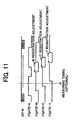
- Fig. 11 is a diagram that shows a timing of a resist adjust processing.
- Fig. 12 is a flowchart that shows an embodiment relating to a resist adjustment.
- the present invention relates to an image formation apparatus (such as a printer, a copying machine, and a facsimile apparatus that employ a tandem image formation system) that line scans an image holder in a predetermined period with a plurality of optical beams emitted corresponding to each image data of a plurality of colors, and forms one image by superimposing written images of respective colors.
- the invention relates to a resist adjusting technique that avoids a distortion that is generated in a formed image due to variations in the writing synchronizing signal of an optical beam of each color due to changes in temperature following time lapse or the like.
- the present embodiment is an application to a color image formation apparatus of an electronic photographing system, and relates to the writing of laser beams used in an image formation process for generating an electrostatic latent image on a photo conductor.
- An outline of a laser beam writing apparatus will be first explained.
- a color image formation according to the writing of laser beams is carried out based on the following method.
- the lighting of an LD (laser diode) is controlled corresponding to image data of each color component.
- An image holder (a photo conductor) provided for each color is main and sub scanned with each optical beam emitted from the LD.
- Aline scanning according to an optical beam is a main scanning, and a scanning according to a relative movement of an image holder to a direction crossing the main scanning line is a sub scanning.
- Written images of respective color components are superimposed.
- Figs. 1A and 1B show an image writing optical system. Laser beams of four colors are allocated with one polygon mirror, and an image of each color is written into each of four photo conductors not shown.
- Fig. 2 shows a perspective view of a part of the image writing optical system.
- a polygon mirror 3 is used in common to allocate four laser beams from an LD unit 1 that has LD (1) to (4).
- the polygon mirror 3 having mirror surfaces 3U and 3D on two upper and lower stages, and a mirror 2 that directs beams to these surface are used, as shown in Fig. 1B.
- the laser beams are allocated to sides A and B, with the polygon mirror 3 as a center, as shown in Fig. 1A.
- respective photo conductors are scanned with optical beams of four colors including yellow (Y), magenta (M), cyan (C), and black (K) .
- Each optical beam of each color is deflected by the polygon mirror 3, passes an f ⁇ lens not shown, is directed to each photo conductor with a return mirror 7, passes through a BTL (barrel toroidal lens) not shown, and is irradiated, as shown in Fig. 2.
- BTL barrel toroidal lens
- the beam scanning directions become opposite between the side A and the side B as shown in Figs. 1A and 1B. Therefore, the upper side in the drawing becomes a front end of the writing at the side A, and the lower side in the drawing becomes a front end of the writing at the side B.
- a predetermined resist is set for each color from a reference position provided on the scanning line.
- a reference position of the resist is a position at which a synchronous detector detects a beam.
- a front end synchronous detector 4 is provided that detects a beam directed from the return mirror 7.
- a back end synchronous detector 5 is provided. When a beam is incident, each synchronous detector generates a synchronous detecting signal.
- the front end synchronous detector 4 at the side A generates DP_UA/DP_DA
- the front end synchronous detector 4 at the side B generates DP_UB/DP_DB
- the back end synchronous detector 5 at the side A generates DP_EA
- the back end synchronous detector 5 at the side B generates DP_EB.
- the synchronous detectors 4 and 5 for upper and lower polygon mirrors are set common at the side A and the side B respectively, thereby to decrease the number of parts and decrease variations between the parts.
- a signal into two synchronous detecting signals (for example DP_UA and DP_DA) at the circuit side. It is possible to carry out this processing according to the conventional technique.
- Fig. 3 shows one example of this. Fig. 3 shows that the same synchronous detector 4 has received DP_UA and DP_DA.
- the synchronous detector 4 receives DP_UA, and then generates a clock CLK_UA synchronous with this signal. Thereafter, the synchronous detector 4 generates a separation GATE signal, and separates a DP_DA signal. Further, the synchronous detector 4 generates a clock CLK_DA in synchronism with this DP_DA signal.
- the back end synchronous detector 5 is used to implement a conventional method of correcting a variation in the magnification of image formation based on synchronous detection at two points together with a synchronous detecting signal that is generated by the front end synchronous detector 4.
- a position of forming each color image on the photo conductor is assigned by setting a predetermined resist, based on the synchronous detecting signal of each color detected by the front end synchronous detector 4 installed as described above.
- a general resist setting method that is used to write an image based on a synchronous detecting signal will be explained.
- a resist adjusting method of the present invention is based on this method.
- a resist is set as a writing starting position.
- a writing signal LGATE is started up after a predetermined time since the front end synchronous detector 4 has output a synchronous detecting signal.
- This writing signal LGATE is a signal that shows an image writing range in the main scanning direction.
- Fig. 4 shows a timing chart of a signal that explains the operation of starting up the writing signal LGATE.
- Fig. 4 shows an example of the operation on the upper polygon mirror surface at the side A in Figs. 1A and 1B.
- LGATE is started up after a predetermined period since the output of the synchronous detecting signal DP_UA.
- a clock (CLK) that synchronizes the phase with the synchronous detecting signal DP_UA is used, and the number of clocks is counted.
- CLK clock
- LGATE is started up, using the synchronous detecting signal DP_UA as a clear signal.
- the circuit can write in a constant area (refer to Fig. 7 and Fig. 8). Therefore, it is possible to shift the writing image to the left and right (in the main scanning direction), by changing the value of the count value n dots.
- this is a known adjusting method that a mark pattern to detect a color distortion is formed on a conveyer belt that conveys a sheet of recording paper, and this mark pattern is detected with a sensor. Based on a result of the detection, each image formation position is corrected.
- a predetermined number of clocks are set for each beam of the four colors, with the front end synchronous detector 4 as a reference position, thereby to determine LGATE.
- a synchronous detecting signal that becomes a reference is determined, and it is checked whether there is a change in the relationship of a synchronous detecting signal of other colors to the synchronous detecting signal that becomes the reference (a reference DP).
- the setting of other colors is adjusted according to this change (hereinafter this method will be referred to as a "reference DP matching method") .
- the change is improved based on this method.
- Fig. 5 shows a timing chart that explains the operation of checking a variation in the timing that a signal of other color is generated relative to the timing of the reference signal, in order to adjust a resist set value of each color.
- the reference DP is set as DP_UA, and a time interval between this DP_UA and synchronous detecting signals of other colors DP_DA, DP_UB, and DP_DB respectively is measured.
- synchronous detecting signals are at ideal positions when an interval between DP_UA and DP_DA is 30 dots, an interval between DP_UA and DP_UB is 4000 dots, and an interval between DP_UA and DP_DB is 5000 dots, respectively.
- a resist set value to generate LGATE (this is LGATE that is counted in the clock of the DP_DA reference) that determines an image area in Fig. 4 is adjusted by subtracting 2 dots from the ideal position (the position before the variation) . With this adjustment, it is possible to return LGATE to the original position by writing a count value starting from -2. For other colors (DP_UB, and DP_DB), it is also possible to return LGATE to the original positions by adjusting resist set values according to measured variation values, when these colors have changed from the ideal positional relationship.
- the counter that measures a time interval uses the reference DP as a clear or load signal, counts by using a clock phase synchronized with this synchronous detecting signal, and stops counting by using synchronous detecting signals of other colors.
- the reference DP and the synchronous detecting signals of other colors are in asynchronous relationship (as a clock phase)
- the counter carries out counting by using other clock that is not synchronous with the reference DP count starting and count stopping both become asynchronous.
- there is a risk that an error that is larger than a dot occurs due to errors occurring in both.
- a target value is set as a resist-adjusted value of each color obtained to avoid a color distortion between a plurality of colors.
- the resist adjusting method of the present invention is basically in line with the above “reference DP matching method”, but can overcome problems that occur from this method.
- a time interval from the occurrence of the reference synchronous detecting signal till the occurrence of a synchronous detecting signal of other color is measured, and the resist is adjusted based on this variation.
- the synchronous detector 4 must be provided on the condition that it is always possible to measure such time interval. This limits the layout of the synchronous detector 4, and it is not possible to take a large degree of freedom of design.
- a mark pulse signal is generated by determining an optional position (a "timing" on the circuit, in actual practice) based on a synchronous detecting signal of other color.
- a matching with the reference DP is carried out according to the generated mark pulse, thereby to eliminate this limit.
- Fig. 6 shows an outline structure of a circuit relating to an image writing processing of the image formation apparatus according to the present invention.
- a circuit of the present embodiment has image writing sections by the number of color components ("4" in the present example).
- the image writing section of each color comprises an LD1 (refer to Figs. 1A and 1B) that generates a writing beam to an image holder such as a photo conductor, an LD driver 13 that controls the light emission of the LD1 with a modulation signal generated based on image data, a synchronous detector 4 (refer to Fig. 1A, Fig. 1B and Fig.
- control circuits 15 to 18 each of which generates a writing signal LGATE for each scanning line based on a synchronous detecting signal from the synchronous detector 4, and transmits image data to the LD driver 13 according to the timing operation of LGATE.
- a CPU 10 has a memory 11 under its control that stores data necessary for operating each section of the apparatus and a program for controlling each section of the apparatus.
- the CPU functions as a system controller that controls the whole apparatus including an image input apparatus (such as a scanner, and a printer controller that receives print data generated at the outside via an I / F) 20 that generates image data that becomes a source of a writing image to be written by the image writing section, the writing control circuits 15 to 18, a polygon motor driving control circuit not shown, and an image holder (such as a photo-sensitive drum) driving motor control circuit not shown.
- the CPU 10 sets operation conditions to the writing control circuits 15 to 18, and transmits a signal necessary to carry out the writing control and image data delivered from the image input apparatus 20, according to an instruction from the console section not shown or an instruction included in the input data.
- the CPU 10 carries out a resist adjustment processing to be described later in detail, by carrying out a matching with the reference DP according to the mark pulse, stores the operation conditions changed based on the adjustment as set data, and reflects the data to the control operation at the image writing time.
- Each of the writing control circuits 15 to 18 includes a circuit that generates LGATE according to a set value as a factor necessary to carry out a normal image writing control, and also includes a circuit that measures time data from the reference DP to the mark pulse signal of other color as a factor necessary to obtain a resist adjustment level.
- a circuit for each color that realizes the writing signal LGATE to be started up after a predetermined time since the front end synchronous detector 4 has output a synchronous detecting signal, in a similar manner to the above (refer to Fig. 4).
- a measuring circuit is structured by determining in advance other colors to be matched with the reference color, in order to use the measurement data to match with the reference DP.
- the following embodiment shows K as the reference, and M, C, and Y as other colors. It is also possible to use other color than K as the reference.
- Fig. 7 shows a circuit structure of the writing control circuit 15 of a reference color in further detail
- Fig. 8 shows a circuit structure of the writing control circuits 16 to 18 of other colors in further detail
- Fig. 8 shows an example that other color is C.
- a similar circuit is structured for M and Y.
- Fig. 9 shows a timing chart of a signal that appears on the circuit in order to explain the operation of the circuits shown in Fig. 7 and Fig. 8.
- each one of the reference color control circuit 15 and the other color control circuits 16 to 18 has a circuit that generates a writing signal LGATE.
- the reference color control circuit 15 generates an own writing signal LGATE using a comparator A>B 28, a comparator A ⁇ B 29, and an AND circuit 22.
- Each of the other color control circuits 16 to 18 similarly generates an own writing signal LGATE using a comparator A>B 35, a comparator A ⁇ B 36, and an AND circuit 39.
- the comparator A>B28 compares a count value of the terminal A with an LGATEON-K value of the terminal B set from the CPU 10 in order to determine a timing (that is, a resist) of starting up LGATE, and outputs a signal that is started up when A>B (Fig. 9(c)).
- the comparator A ⁇ B29 compares a count value of the terminal A with an LGATEOFF-K value of the terminal B set from the CPU 10 in order to determine a timing of falling LGATE, and outputs a signal that falls when A ⁇ B (Fig. 9(d)).
- An AND circuit 22 takes AND of the outputs of both comparators 28 and 29. Therefore, the output becomes a writing signal LGATE-K (Fig. 9(e)) that determines an image writing period, and is used by the LD driver 13 as an image writing signal of K.
- a mark pulse signal is generated by determining an optional position (a "timing" on the circuit, in actual practice) based on a synchronous detecting signal that is generated for each color. A matching with the reference DP is carried out according to the generated mark pulse.
- a mark pulse is generated, and it is checked whether the timing of the generated mark pulse and the timing of the reference DP are in a predetermined relationship.
- This checking is carried out by measuring a pule interval between the mark pulse and the pulse of the reference DP (hereinafter to be referred to as a "mark interval measurement").
- DP-C is input to the terminal A of this comparator 37.
- DP-C is a synchronous detecting signal of C, that is a count value of CLK-C generated by phase synchronizing (k) in Fig. 9 using DP-C as a clear signal. In other words, this is time data from DP-C same as that used to generate LGATE in the above.
- the MARK-C signal generated above is transferred to the reference color control circuit shown in Fig. 7 (shown by 15 in Fig. 6), and is used to measure a timing relative to the timing of the reference DP (DP-K).
- a MARK-M signal and a MARK-Y signal (Fig. 9(g) and (i)) that are output are sent to the reference color control circuit in a similar manner, for M and Y.
- latches 25 to 27 structure a unit for this in the reference color control circuit shown in Fig. 7.
- DP-K is input to the latches 25 to 27.
- DP-K is a synchronous detecting signal of K, that is a count value of CLK-K generated by phase synchronizing (b) in Fig. 9 using DP-K as a clear signal.
- this is time data from DP-K same as that used to generate LGATE in the above.
- This input time data is latched using a mark pulse signal as a stop signal. Based on the latch, the "mark interval measurement" is carried out, and it becomes possible to obtain this data.
- the MARK-C signal When the color is C, the MARK-C signal is latched as a stop signal, and CNT-C is obtained as "mark interval measurement" data from the reference DP.
- This data includes a deviation ( ⁇ n in Fig. 9 (h)) in the output timing of the MARK-C signal due to time lapse. Therefore, this data is sent to the CPU 10 in order to carry out a resist adjustment.
- the CPU 10 receives CNT-C, CNT-M, and CNT-Y (time data from the reference DP to the other color mark pulse signal) measured by the reference color control circuit 15.
- the CPU 10 checks whether the measured "mark interval measurement” data (CNT-C, CNT-M, and CNT-Y) coincides with a set target value of the resist condition that there is no color distortion.
- the CPU 10 corrects the set data (MARK ON, LGATE ON) to coincide with the target value.
- the target value there is used a value that has been experimentally confirmed based on the resist condition that no color distortion occurs.
- a value obtained at the plant shipment time is used based on a known adjusting method of matching each color with a reference mark provided on the surface of an image holder on which an image is actually formed, such as a belt surface when a transfer belt is used.
- a value determined based on experience may be used.
- a difference between the temperature and the target value may be prepared as a temperature table in advance. It is possible to set a suitable target value by referring to this table based on the temperature at the adjusting time. Further, based on the default value determined above, a user may update the last target value using a value adjusted in different using conditions, thereby to set a new target value.
- MARK ON data is corrected according to a difference between the set target value and the measured "mark interval measurement”.
- the "mark interval measurement” data (CNT-C, CNT-M, and CNT-Y) changes based on the corrected data. Therefore, measurement is carried out again, and coincidence with the target value is checked again. The data correction is continued until when these values coincide with each other.
- Fig. 10 shows an embodiment of a flowchart relating to a resist adjustment processing.
- the resist condition that no color distortion occurs is obtained as described above, and a target value (n0) stored in the memory is loaded to use it in this processing (S1).
- the target value (n0) is the target value corresponding to the "mark interval measurement" data (CNT-C, CNT-M, and CNT-Y) .
- step S12 After carrying out the adjustment processing, the process returns to step S12 to carry out the processing to confirm whether the "mark interval measurement" data (CNT-C, CNT-M, and CNT-Y) coincides with the target value based on the data after the adjustment within the limit of m times.
- the measurement and checking are repeated (S12 and 13) to avoid error for better adjustment.
- the data of the difference (n0 - ni) to be used for the correction to make the "mark interval measurement" data (CNT-C, CNT-M, and CNT-Y) coincide with the target value is calculated. Then, the set values of new MARK ON data and LGATE ON data are obtained. It is possible to carry out this processing at an optional timing when the reference DP (a synchronous detecting signal) and a DP of other color are output. Therefore, it is preferable to be able to calculate at least the "mark interval measurement” and the difference value (n0 - ni) even during the image writing, thereby to improve the total processing efficiency.
- Fig. 11 is a diagram that explains the timing of this processing.
- DP-K is always output as well as DPs of other colors. Therefore, it is possible to select an optional measuring timing for carrying out the "mark interval measurement” and the calculation of the difference value (n0 - ni) , even when image writing periods (frame period) of colors FGATE-K, M, C and Y are ON.
- the resist adjustment of M, C and Y that is, the changing of the setting of the LGATE ON data after the adjustment, is carried out while FGATE-M, C and Y are OFF.
- the environmental temperature changes the refractive index of the lens that focuses a beam emitted from the LD on the scanning line of the photo conductor as a spot beam. Therefore, the magnification of the image to be formed changes due to the temperature.
- This has been conventionally correctedby changing the frequency of pixel click.
- different frequencies are used among colors. For example, the clock frequency fk of K and the clock frequency fc of C become fk ⁇ fc.
- the resist adjustment method based on the "mark interval measurement" of the present invention for measuring the timing of the mark pulse signal relative to the timing of the reference DP (DP - K), it is possible to absorb this variation.
- the environmental temperature expands and contracts the optical housing along a change in temperature, and this changes the position of the synchronous detector 4.
- a color distortion occurs, as a resist is determined from the synchronous detecting signal DP of each color.
- the resist adjustment method based on the "mark interval measurement" of the present invention for measuring the timing of the mark pulse signal relative to the timing of the reference DP (DP - K), it is also possible to avoid this variation by adjustment.
- the resist adjustment according to the "mark interval measurement" of the present invention is effective for temperature compensation. Therefore, for instructing the execution of the resist adjustment, it is necessary to improve the performance of the apparatus by selecting a suitable timing.
- the suitable timing is the timing when there is a possibility of the occurrence of a change in the environmental temperature. This timing is different depending on how the target value of resist adjustment is set or depending on the using environment. There is a high possibility that a resist distortion occurs due to a change in temperature, at the time of starting up the power source of the apparatus or at the time of starting the image formation. Therefore, adjustment is carried out at least at this timing.
- the CPU 10 starts the resist adjustment processing when it has received a recognition signal of this timing based on the turning ON of the power source with the ON/OFF key, the depression of the start key of the copying machine or the printer, or the reception of a print request instruction from the outside.
- a timing at which adjustment becomes necessary is caught through the monitoring of a change state. For example, time lapse or an image formation processing level (for example, a number of copied sheets of paper) is detected after starting the image formation. When a preset value has changed, the adjustment is started.
- time lapse or an image formation processing level for example, a number of copied sheets of paper
- Fig. 12 shows a resist adjustment flow relating to this embodiment.
- a set value A that is preset as a timing at which adjustment becomes necessary is loaded to use it in this processing (S21).
- This set value is a time lapse or a number of copied sheets of paper since the starting of the image formation processing.
- the resist adjustment is started.
- the above resist adjustment processing sequence (refer to Fig. 10) is carried out (S24). After confirming the completion of the resist adjustment (S25), the flow ends.
- the resist adjustment is executed at a timing of high possibility of the occurrence of a color distortion. Based on this, it becomes possible to prevent a color distortion in advance without increasing the processing load of normal execution.
- the image formation process for forming a color image on a sheet of transfer paper by matching images of various color components can be executed by applying a method that is used in an existing tandem system color laser printer, color copying machine or the like.
- a mark pulse signal is generated by determining an optional position based on a synchronous detecting signal (DP) that is generated for each color.
- a matching with the reference DP is carried out according to the generated mark pulse, thereby to eliminate constraint of the layout of synchronous detecting signals. Therefore, based on a simple system, it is possible to avoid the conventional problems that a mark pattern is actually written and a distance between marks is measured, thereby requiring a whole apparatus. It is possible to carry out resist adjustment within the apparatus, and it is possible to adjust corresponding to a time lapse change such as the environmental temperature. Consequently, it is always possible to form an image without any color distortion.
- the "mark interval measurement” is carried out by using an image writing clock that is synchronous with the reference DP, it is possible to keep the measurement precision at a constant level, and can guarantee formation of high-quality image as a result.
- the invention is applied to an image formation apparatus of the system that carries out simultaneous writing to each image holder by using a common rotational polygon mirror, it is possible to realize the above effect in a high-speed apparatus. Further, it becomes possible to achieve high performance.
Landscapes
- Engineering & Computer Science (AREA)
- Physics & Mathematics (AREA)
- General Physics & Mathematics (AREA)
- Signal Processing (AREA)
- Optics & Photonics (AREA)
- General Engineering & Computer Science (AREA)
- Multimedia (AREA)
- Theoretical Computer Science (AREA)
- Laser Beam Printer (AREA)
- Facsimile Scanning Arrangements (AREA)
- Fax Reproducing Arrangements (AREA)
- Mechanical Optical Scanning Systems (AREA)
- Facsimile Heads (AREA)
- Color, Gradation (AREA)
- Color Image Communication Systems (AREA)
Applications Claiming Priority (2)
| Application Number | Priority Date | Filing Date | Title |
|---|---|---|---|
| JP2001302596 | 2001-09-28 | ||
| JP2001302596A JP2003103829A (ja) | 2001-09-28 | 2001-09-28 | 画像形成装置及びレジスト調整方法 |
Publications (2)
| Publication Number | Publication Date |
|---|---|
| EP1298577A2 true EP1298577A2 (fr) | 2003-04-02 |
| EP1298577A3 EP1298577A3 (fr) | 2003-04-09 |
Family
ID=19122810
Family Applications (1)
| Application Number | Title | Priority Date | Filing Date |
|---|---|---|---|
| EP02021833A Withdrawn EP1298577A3 (fr) | 2001-09-28 | 2002-09-27 | Synchronisation des couleurs dans des imprimantes à laser |
Country Status (3)
| Country | Link |
|---|---|
| US (1) | US6788320B2 (fr) |
| EP (1) | EP1298577A3 (fr) |
| JP (1) | JP2003103829A (fr) |
Cited By (1)
| Publication number | Priority date | Publication date | Assignee | Title |
|---|---|---|---|---|
| EP1783665A1 (fr) * | 2005-11-01 | 2007-05-09 | Ricoh Company, Ltd. | Appareil et méthode de contrôle des instants de démarrage de formation d'image et imprimante associée |
Families Citing this family (4)
| Publication number | Priority date | Publication date | Assignee | Title |
|---|---|---|---|---|
| US6842187B2 (en) * | 2003-05-02 | 2005-01-11 | Kabushiki Kaisha Toshiba | Optical beam scanning device and image forming apparatus |
| JP4324488B2 (ja) * | 2003-07-07 | 2009-09-02 | 株式会社リコー | 画像形成装置 |
| US7589846B2 (en) * | 2004-06-30 | 2009-09-15 | Ricoh Company, Ltd. | Method and apparatus for image forming capable of effectively correcting alignment errors of elementary color outputs to be superposed into an image |
| JP2007133238A (ja) * | 2005-11-11 | 2007-05-31 | Ricoh Co Ltd | 画像形成装置および色ずれ補正方法 |
Family Cites Families (15)
| Publication number | Priority date | Publication date | Assignee | Title |
|---|---|---|---|---|
| US4967284A (en) | 1987-10-19 | 1990-10-30 | Ricoh Company, Ltd. | Image forming apparatus and method of controlling output of semiconductor laser |
| JPH07101417B2 (ja) | 1987-12-11 | 1995-11-01 | 株式会社日立製作所 | 蓄積データの再利用方法 |
| US5027117A (en) | 1988-03-31 | 1991-06-25 | Ricoh Company, Ltd. | Conversion using a variable reference based on image density |
| JP2677814B2 (ja) | 1988-04-07 | 1997-11-17 | 株式会社リコー | 記録装置 |
| JPH0377473A (ja) | 1989-08-21 | 1991-04-03 | Ricoh Co Ltd | 画像情報記憶装置 |
| US5212570A (en) * | 1991-06-27 | 1993-05-18 | Xerox Corporation | Pixel clock phase locked loop for a laser scanner |
| JP3231856B2 (ja) | 1991-10-31 | 2001-11-26 | 株式会社リコー | 画像形成装置 |
| US5376994A (en) | 1992-02-13 | 1994-12-27 | Ricoh Company, Ltd. | Compact BI-color electrophotographic image forming apparatus |
| JP2948704B2 (ja) * | 1992-09-21 | 1999-09-13 | 富士写真フイルム株式会社 | 複数光ビームの露光方法 |
| JP3698490B2 (ja) | 1996-07-15 | 2005-09-21 | 広利 増田 | 門型側溝の施工法 |
| JP3998760B2 (ja) * | 1997-08-01 | 2007-10-31 | 株式会社リコー | 多色画像形成装置 |
| JP3519255B2 (ja) * | 1997-10-31 | 2004-04-12 | シャープ株式会社 | 画像形成装置 |
| EP0985980B1 (fr) * | 1998-09-07 | 2010-02-10 | Sharp Kabushiki Kaisha | Appareil de formation d'images à couleurs |
| JP2000235290A (ja) * | 1998-12-17 | 2000-08-29 | Fuji Xerox Co Ltd | 画像形成装置 |
| JP3772607B2 (ja) | 1999-10-25 | 2006-05-10 | 富士ゼロックス株式会社 | 多色画像形成装置 |
-
2001
- 2001-09-28 JP JP2001302596A patent/JP2003103829A/ja active Pending
-
2002
- 2002-09-27 EP EP02021833A patent/EP1298577A3/fr not_active Withdrawn
- 2002-09-30 US US10/259,384 patent/US6788320B2/en not_active Expired - Fee Related
Cited By (2)
| Publication number | Priority date | Publication date | Assignee | Title |
|---|---|---|---|---|
| EP1783665A1 (fr) * | 2005-11-01 | 2007-05-09 | Ricoh Company, Ltd. | Appareil et méthode de contrôle des instants de démarrage de formation d'image et imprimante associée |
| US7576764B2 (en) | 2005-11-01 | 2009-08-18 | Ricoh Co., Ltd. | Device and method for controlling timing for starting image formation, and an image forming apparatus using such device and method |
Also Published As
| Publication number | Publication date |
|---|---|
| US6788320B2 (en) | 2004-09-07 |
| US20030063178A1 (en) | 2003-04-03 |
| JP2003103829A (ja) | 2003-04-09 |
| EP1298577A3 (fr) | 2003-04-09 |
Similar Documents
| Publication | Publication Date | Title |
|---|---|---|
| KR100846378B1 (ko) | 화상 형성 장치 및 형성 화상 보정 방법 | |
| EP1392049B1 (fr) | Appareil de formation d'image | |
| US7212224B2 (en) | Pixel clock creation method, pixel clock creation device, optical scanning device, and image forming apparatus | |
| US20010028387A1 (en) | Light beam magnification error auto correcting apparatus and method | |
| JP2013117699A (ja) | 画像形成装置 | |
| JP2006205400A (ja) | 画像形成装置、プリンタ装置、ファクシミリ装置、及び、複写機。 | |
| EP1355482B1 (fr) | Dispositif de balayage optique et dispositif de formation d'image avec ce dispositif | |
| US6788320B2 (en) | Image formation apparatus and registration method | |
| US20050036028A1 (en) | Image-forming apparatus and optical scanner | |
| JP5005221B2 (ja) | 画像形成装置、画像形成方法、プログラム及びコンピュータ読取可能な記録媒体 | |
| JPH1155472A (ja) | 多色画像形成装置 | |
| JP4546845B2 (ja) | 光ビーム走査装置、画像形成装置及び倍率誤差補正方法 | |
| JP3499984B2 (ja) | 画像形成装置 | |
| JP4321763B2 (ja) | 光走査装置および画像形成装置 | |
| JP4250575B2 (ja) | カラー画像形成装置 | |
| JPH0985989A (ja) | 画像形成装置 | |
| US8054502B2 (en) | Scanning optical apparatus, image forming apparatus and image clock correction method | |
| JP2004354626A (ja) | 画像形成装置及び該装置における水平同期信号発生方法 | |
| JP2001013430A (ja) | マルチビーム画像形成装置 | |
| JP2006181835A (ja) | 画像形成装置 | |
| JP2003154703A (ja) | 画像形成装置 | |
| JP4150862B2 (ja) | 画像形成装置 | |
| JP2005062714A (ja) | ビーム走査装置 | |
| JP4400386B2 (ja) | 画像処理装置及び画像処理方法 | |
| JP2006251019A (ja) | 画像形成装置 |
Legal Events
| Date | Code | Title | Description |
|---|---|---|---|
| PUAI | Public reference made under article 153(3) epc to a published international application that has entered the european phase |
Free format text: ORIGINAL CODE: 0009012 |
|
| PUAL | Search report despatched |
Free format text: ORIGINAL CODE: 0009013 |
|
| AK | Designated contracting states |
Kind code of ref document: A2 Designated state(s): AT BE BG CH CY CZ DE DK EE ES FI FR GB GR IE IT LI LU MC NL PT SE SK TR Designated state(s): AT BE BG CH CY CZ DE DK EE ES FI FR GB GR IE IT LI LU MC NL PT SE SK TR |
|
| AX | Request for extension of the european patent |
Extension state: AL LT LV MK RO SI |
|
| AK | Designated contracting states |
Kind code of ref document: A3 Designated state(s): AT BE BG CH CY CZ DE DK EE ES FI FR GB GR IE IT LI LU MC NL PT SE SK TR |
|
| AX | Request for extension of the european patent |
Extension state: AL LT LV MK RO SI |
|
| RIC1 | Information provided on ipc code assigned before grant |
Ipc: 7H 04N 1/50 B Ipc: 7G 06K 15/12 A |
|
| 17P | Request for examination filed |
Effective date: 20030509 |
|
| AKX | Designation fees paid |
Designated state(s): DE FR GB |
|
| 17Q | First examination report despatched |
Effective date: 20071214 |
|
| STAA | Information on the status of an ep patent application or granted ep patent |
Free format text: STATUS: THE APPLICATION HAS BEEN WITHDRAWN |
|
| 18W | Application withdrawn |
Effective date: 20090525 |