EP1298852A2 - Système et méthode de commande de Multi-subshelf pour un élément de réseau - Google Patents
Système et méthode de commande de Multi-subshelf pour un élément de réseau Download PDFInfo
- Publication number
- EP1298852A2 EP1298852A2 EP02292371A EP02292371A EP1298852A2 EP 1298852 A2 EP1298852 A2 EP 1298852A2 EP 02292371 A EP02292371 A EP 02292371A EP 02292371 A EP02292371 A EP 02292371A EP 1298852 A2 EP1298852 A2 EP 1298852A2
- Authority
- EP
- European Patent Office
- Prior art keywords
- slave
- controller
- commands
- communication
- shelf
- Prior art date
- Legal status (The legal status is an assumption and is not a legal conclusion. Google has not performed a legal analysis and makes no representation as to the accuracy of the status listed.)
- Granted
Links
Images



Classifications
-
- H—ELECTRICITY
- H04—ELECTRIC COMMUNICATION TECHNIQUE
- H04L—TRANSMISSION OF DIGITAL INFORMATION, e.g. TELEGRAPHIC COMMUNICATION
- H04L49/00—Packet switching elements
- H04L49/25—Routing or path finding in a switch fabric
- H04L49/253—Routing or path finding in a switch fabric using establishment or release of connections between ports
- H04L49/254—Centralised controller, i.e. arbitration or scheduling
-
- H—ELECTRICITY
- H04—ELECTRIC COMMUNICATION TECHNIQUE
- H04L—TRANSMISSION OF DIGITAL INFORMATION, e.g. TELEGRAPHIC COMMUNICATION
- H04L49/00—Packet switching elements
- H04L49/55—Prevention, detection or correction of errors
- H04L49/555—Error detection
-
- H—ELECTRICITY
- H04—ELECTRIC COMMUNICATION TECHNIQUE
- H04L—TRANSMISSION OF DIGITAL INFORMATION, e.g. TELEGRAPHIC COMMUNICATION
- H04L49/00—Packet switching elements
- H04L49/60—Software-defined switches
- H04L49/602—Multilayer or multiprotocol switching, e.g. IP switching
Definitions
- the invention relates to a system and method providing a multi-subshelf communication system for a network element of a communication network.
- a multi-shelf communication system for a communication switch having comprising a plurality of shelves.
- the communication system comprises a master controller generating commands and receiving status signals, slaves associated with the master controller, a communication controller for each slave, a downstream communication link comprising a multiplexed signal gathering communications from each communication controller into a single multiplexed stream and providing a demultiplexed signal split from the single multiplexed stream to each slave, an upstream communication link from each slave to its communication controller, and a timing arrangement controlling transmission times of communications carried on the downstream communication link.
- Each slave can be located on one the shelves and receives commands, executes local commands responsive to the commands and generates status signals for the master controller.
- Each communication controller receives commands, transmit the commands to its slave, receives status signals and provides information relating to the status signals to the master controller.
- the local commands executed by the slaves replace other commands directed by the master controller to the slave.
- Each slave communicates independently with the master controller.
- the system may have the timing arrangement utilizing a time division multiplex scheme.
- the system may have the upstream communication link comprising a multiplexed signal gathering communications from each the slave device into a second single multiplexed stream and providing a second demultiplexed signal split from the second single multiplexed stream to each communication controller.
- the system may have the master controller associated with a control card for the communication switch.
- the system may have at least one slave as a fabric interface card.
- the system may have at least one slave as a line card.
- the system may synchronize communications carried in the downstream communication link and the upstream communication link.
- the system provides a multi-shelf communication arrangement of devices in a communication switch.
- the arrangement is a master-slave system where a controller is provided as the master controller and a plurality of devices are the slave devices.
- switch 100 is a multi-protocol backbone system, which can process both of ATM cells IP traffic through its same switching fabric for customer premise equipment (CPE) 102 connected thereto.
- CPE customer premise equipment
- switch 100 provides CPEs 102 with access to its switching fabric 104 which is the core of switch 100.
- the switching fabric 104 provides a matrix allowing each CPE 102 to be connected to other devices connected to the switch 100.
- switch 100 allows scaling of the switching fabric capacity from 50 Gbps to 450 Gbps in increments of 14.4 Gbps by the insertion of additional shelves into the switch 100.
- CPEs 102 are connected to switch 100 via optical links 106 to I/O cards 108.
- I/O cards 108 provide the main input and output interface for conversion of communications between CPEs 102 and switch 100. I/O cards 108 provide minimal intelligent processing of communications passed therethrough.
- I/O cards 108 are connected to line cards 110 via midplane connections 112. Each line card 110 provides OC-192 functionality, bandwidth provisioning and ATM processing of cells between core of switch 100 and each CPE 102.
- Each line card is also connected to a fabric interface card (FIC) 114, which converts the signal to an optical signal and provides an interface for the communications with core 104.
- FIC fabric interface card
- the FIC can monitor and react to conditions reported by the line card 110.
- the FIC 114 may analyze and respond to failures reported by its line card 110, conduct sanity checks on data received from its line card 110 and send reporting messages to upstream shelf controller (described later).
- FICs 114 communicate with LPC 110 via midplane connections 116 and with core 104 via connections 118.
- the interface to core 104 for each FIC 114 is a switch access card (SAC) 120.
- SAC switch access card
- each I/O card 108, line card 110 and FIC 114 has a redundant counterpart, which is noted with the 'b' suffix. Accordingly, midplane connections 112 and 116 provide cross connections between the redundant and primary devices. For example, I/O cards 108 and 108b are connected to line cards 110 and 110b and line cards 110 and 110b are connected to FICs 114 and 114b.
- I/O card 108, line card 110 and FIC card 114 are grouped together in a single high speed peripheral shelf (HSPS) 122.
- HSPS 122 has two sets of I/O card groupings in slots 126 to provide redundancy between the groups of shelves.
- Switch 100 enables the use of multiple HSPSs 122 to provide enhanced expandability for the switch. Accordingly, with components grouped into shelves, a number of individual shelves can populate a switch 100 to provide modular functionality for switch 100.
- control signals for each shelf are also provided in modules, as necessary. This entails separate cabling of bundled control signals to each shelf at a communications point on each shelf. From the communication point, individual signals for individual components in the shelf are isolated and forwarded accordingly.
- Each I/O card 108 grouping in HSPS 122 must be controlled and co-ordinated with the other I/O cards 108 in HSPS 122.
- the embodiment provides a shelf controller 124 which controls operating aspects of shelves 122 connected to it.
- Such control operations include managing control and status functions for the shelf (such as slot monitoring and fan unit control), controlling FIC configuration for each line card 108, power rail monitoring and clock signal monitoring.
- Shelf controller 124 provides control connectivity via a specialized control service link (not shown). Data carried in the control service link controls downstream configuration and software downloading, time stamping, and synchronization of clocks.
- a terminal 128 is connected to switch 100 and runs controlling software which allows an operator to modify, and control the operation of, switch 100.
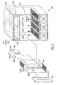
- switch 100 physically comprises a chassis 200, which houses HSPS 122 in cavity 202.
- HSPS 122 is contained in housing 204, which sits in a section of cavity 202.
- Shelf controller 124 is located above cavity 202.
- Each housing 204 contains a midplane 206, which is a physical support structure having connectors allowing line cards 110, FICs 114 and I/O cards 108 to be connected thereto. Connections 112 and 116 (see, Fig. 1) are provided by appropriate electrical connections between connectors in midplane 206.
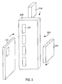
- view 300 illustrates line card 110, I/O card 104, and FIC card 108 and midplane 206 for housing 204.
- Cards that have optical interfaces namely the I/O card 104 and FIC card 108, are located on one side of the midplane 206 and line card 110 is located on the other side of the midplane 206.
- Connectors 208 provide the physical interface for the cards to midplane 206. Specific connections between I/O card 104 and line card 110 and FIC card 108 are provided from the pins of various connectors 208 through midplane 206.
- switch 100 may be used to describe switch 100. Further, while the embodiment is described for switch 100, it will be appreciated that the system and method described herein may be adapted to any switching system.
- a mechanism for providing instructions from the shelf controller 124 to each line card 110 there is a need to have a mechanism for providing instructions from the shelf controller 124 to each line card 110.
- the remote line card was dumb, having no processing capabilities, e.g. a typical I/O card, or alternatively, all of the intelligence was placed on the line card, e.g. a typical line card or a FIC.
- the computing power required at the processing end becomes too large for the processing entity.
- the embodiment utilizes a system wherein computing is distributed between the FIC 114 and the shelf controller 124.
- the shelf controller 124 identifies what actions need to be taken by a FIC 114 and sends an appropriate instruction to the FIC 114.
- Each FIC 114 receives and processes its instruction and provides a suitable response to the shelf controller 124.
- the "master” element is the operative element in the shelf controller 124 and the “slave” element is the FIC 114.
- the term “master” is used interchangeably with “shelf controller” and the terms “slave” and “FIC” are also interchangeable for this specification. It will be appreciated that in other embodiments, the slave may be line card 110 or any other downstream device to the master.
- the embodiment provides an egress communication system 400 for each HSPS 122 and the shelf controller 124.
- master controller 402 produces individual commands for each FIC 114 in each subshelf 122.
- Communication controllers 404 in shelf controller 124 receive each command for each FIC, or slave 114 and has them sent to each slave 114.
- Each HDLC communication controller 404 communicates with the FIC cards in slave 114 to request read/write access to FIC registers (not shown). For example, on a "read" command, master controller 402 may require status data about slave device 114a. In the distributed system, master controller 402 generates a read command for a particular flag of slave device 114a.
- Communication controller 404a receives the command from master controller 402 and has the command sent, ultimately, to slave device 114a, which receives the read command and processes it. After the read command is processed by slave device 114a, a response is generated and is sent back to master controller 402 through an ingress communication system 500, which provides an ingress communication link from each slave device 114a to controller 404a.
- Each controller 402 uses HDLC (High Level Data Link Control) protocol.
- HDLC is a known ISO and ITU-T standaridized link layer protocol used in point-to-point and multi-point communications.
- HDLC provides bit-oriented synchronous transmission of variable length frames.
- master 124 has unbalanced links with slaves 114. Accordingly, master 124 polls each slave 114 as necessary, and each polled slave 124 responds with information frames. The master 124 then acknowledges receipt of the frames from the slave. It will be appreciated that other communication protocols may be used. It will be appreciated that as there is a dedicated master for each slave, collectively, polling amongst all slaves can be done concurrently.
- the field length (in bits) is variable, depending on the HDLC control field.
- master 404 may request to a slave 114 to respond with a report of the status of all interrupts on slave card 114. Accordingly, the slave 114 would read all its registers that contain an interrupt status.
- An interrupt status may, for example, store the change of state information of an optical signal received by a pin diode.
- the slave 114 collects the register information and transmits it to master 402 per the designed communication protocol. It will be appreciated that this distributed messaging system overall provides a faster response time than have a master communicate with each slave device individually to and read their register status.
- the master can collect all slave 114 information, then provide a response based on the net status of all slave registers.
- the control field is set to 00000000 by software in master controller 402 and the data field is defined as 32 bits containing an embedded 16 bit slave address as shown below:
- each communication controller 404 is individually hardwired to each slave 114 with links 405.
- multiplexing of signalling links is provided on both the ingress and egress directions. This is shown in Fig. 4B.
- each communications controller 404 receives instructions from master controller 402; each HDLC controller 404 is connected to multiplexer 406, producing one serial stream of data containing N channels of data on serial link 408.
- microprocessor 420 is a MPC 8260 Power PC PowerQUICC II programmable processor, available from Motorola, Inc.
- Microprocessor 420 has a programmable multichannel controller (MCC). The embodiment configures the MCC to provide the 16 communication controllers 404.
- MCC programmable multichannel controller
- microprocessor 420 also has an internal multiplexer 406 to produce single datastream 408 from the datastreams produced by the communication controllers 404.
- microprocessor 420 has a time slot assignor 421 which assigns a 8-bit timeslot from the TDM stream 408 to each of the controllers 404.
- the stream contains sixteen 8 bit slots operating at 8.25 MHz.
- the TDM stream in link 408 comprises 16 serial packets as shown below: It is desirable to have the HDLC timeslot at a minimum length (and thus the TDM stream at a minimum length) to decrease the latency on timesensitive information in the TDM stream (such as interrupt status).
- Serial link 408 is provided to a group demultiplexer 410 which collectively groups the N channels into M channels 412.
- the demultiplexer 410 is embodied in a field programmable gate array (FPGA) 410.
- FPGA field programmable gate array
- Control for demultiplexer 410 is fixed and the demultiplexing does not change on different conditions.
- a bit counter signal and a channel counter signal are associated with the TDM stream.
- the bit counter signal and the channel counter signal are used by demultiplexer 410 to identify which bits from controllers 404 (or which bits from registers within FPGA 410) are inserted into which channel 412 at the correct frame.
- the FPGA 410 provides the following functions for microprocessor 406.
- the TDM stream 408 between the microprocessor 420 and FPGA 410 contains HDLC interfaces for FIC communications.
- the FPGA splits out TDM stream 408 into individual MTDM streams 412 for each of the HSPS sub-shelves 122.
- Control signals are embedded into the TDM stream 408 by FPGA 410.
- control signals for a FIC such as Line Card Presence, sub-shelf Number, FIC Interrupt Status, etc. may be transmitted between microprocessor 420 and slave 110 using the signal multiplexing scheme and FPGA 410.
- Microprocessor 420 provides a request for control signals for a FIC to FPGA 410 sent via 60x bus 422.
- FPGA 410 inserts an appropriate request in the appropriate timeslot for the requested slave 114 in the appropriate egress datastream 412.
- the targetted slave responds to the request and transmits the status to FPGA 410 via the ingress multiplexed stream.
- the results are stored in FPGA registers, which can be accessed by microprocessor 420 over bus 422.
- FPGA 420 may send a (maskable) interrupt to microprocessor 420 upon a status change of a control signal.
- FPGA 410 also performs a digital phase comparisons of the selected sources of timing from the shelf 124 and compares it with the system source sent to the shelf.
- TDM streams 412 connect the shelf controller to each of the four subshelves.
- the second TDM stream is a 16 timeslot frame operating at 8.25 MHz for each subshelf 122.
- Each M channel 412 is provided to each subself 122.
- Each of the four TDM substreams 412 (one to each sub-shelf) is a 16 timeslot frame operating at 8.25 MHz.
- TDM demultiplexer 414 utilizes the bit counter signal and the channel counter signal to determine which incoming part of the datastream on channel 412 is sent on which outgoing channel 416.
- demultiplexer 414 receives each channel 412 and produces N / M separate communication links 416, each of which is provided to each slave 114.
- Each slave device 114 has a HDLC interface module 418 which translates the HDLC encoded datastream 416 into a format which can be used by each slave 114.
- Each communication controller 404 has a timeslot in the TDM stream assigned to it. Similarly, each slave device 114 has a timeslot assigned to it for sending information to the master controller. Also, slave devices 114 can interrupt the master controller 124 at any time, if required.
- Having a dedicated communications controller 124 and corresponding control bandwidth for each slave device 114 ensures that control commands from the master controller 402 will be received by the slave devices 114 within a deterministic amount of time.
- each slave 114 generates a response or a signal destined for master controller 402; each slave 114 is to multiplexer 702, producing one serial stream of data containing N / M channels of data on serial link 704.
- Serial link 704 is provided to FPGA 410 which processes the information in the N / M channels 704 and provides an appropriate response, if necessary to master controller 402 via 60x bus 422.
- each slave device 114 Since each slave device 114 has its own timeslot during which it can communicate with the controller 402, information from the slave devices 110 will reach the master controller 402 within a defined amount of time. This allows bidirectional communications between the slave devices and the master controller to occur within a guaranteed latency. Accordingly, the embodiment allows a multishelf platform to detect a fault within 10 ms re-route around the fault within 50 ms, thereby conforming with requirements of a carrier-grade system.
- ingress multiplexing system 700 shares functional similarities with egress system 400.
- line cards 110 and I/O cards 108 generate some status signals as dc signals (not shown) which are provided to their CPLD 702.
- Each CPLD may embed these signals into the datastreams of its respective channel 704.
- FPGA 706 these embedded signals may be extracted and processed locally as needed. For example, they may be provided to other cards and systems associated with the FPGA 706.
- an ingress signalling system is also provided, which is similar to egress system 400, and is described later.
- each TDM bus is configured according to the following timing parameters.
- Each multiplexer has access to these timing signals.
- a common clock 602 operates at 8.25MHz and a frame pulse (FP) 604 operates at 64.45KHz.
- FP frame pulse
- the rising edge of FP 604 is aligned to the rising edge of clock 602.
- the FP defines a frame for a byte of transmitted information.
- timeslot signal 608 In order to provide the system with an earlier indication of the arrival of the next timeslot, timeslot count signal 608 in generated which is the same count signal as timeslot signal 606, but it is generated half a clock cycle earlier.
- bit position signal 610 As with the timeslot signal 606, as a mate to bit position signal 610, bit position count signal 612 is generated to provide the system with an earlier indication of the arrival of the next bit position.
- the first bit of the first timeslot (bit 7 of timeslot 0) is the MSB and will be coincident with the rising edge of FP 406. As there are 8 bits of data per timeslot, for data transactions involving data fields of more than 8 bits requires more than 1 TDM slot. Successive required slots are provided in the next TDM superframe.
- timing of signals sent between shelf controller 124 to each of subshelf 104 requires that no cells be dropped. Timing is handled in the following manner.
- each HDLC stream is transmitted at a clocking rate of 8.25 MHz / 16, i.e. approximately 516 kHz (or "R" for "Rate"), to multiplexer 406.
- the collective datastream is clocked at 16 x R on serial link 408 to ensure that successive packets from each controller 404 in successive frames are not lost.
- the collective datastream on link 408 is provided to FPGA 410 which splits datastream into four separate datastreams on channels 412.
- Each separate datastream on each channel 412 contains datastreams for 4 HDLC slots destined for demultiplexers 414 associated with each subshelf 122.
- the clocking rate for each datastream on each channel 412 is still 16R. Accordingly, there is additional bandwidth available in each datastream in each channel 412, as only four slots are needed in the time frame which contains 16 time slots. Accordingly, 12 control slots are added to each datastream in each channel 412 by FPGA 410. The control slots contain information embedded into them by FPGA 410.
- each datastream is then passed to a CPLD within demultiplexer 414, which can extract some of the control information from the datastream for the FIC 114 or line card 110.
- the CPLD is located on midplane 206.
- the CPLD 414 further splits the datastream into four sub datastreams on channels 416, 1 channel 416 per slave device 114.
- a second CPLD (#2) can extract further control information from the received datastream.
- the received HDLC datastream is then clocked-down to the original clocking rate of 8.2MHz / 16, i.e. approximately 516 kHz (R).
- the clocked-down data for data transmissions received by a slave device 114 contains the original information embedded in the TDM stream from its corresponding controller 404a.
- timing is maintained for the data rate and additional control information is provided in each datastream without occupying "true" bandwidth from the master-slave communication link.
- each HDLC link is dedicated, so if all 16 FIC 114 were reporting to their respective masters 404, the total maximum service time is still 188.8 ⁇ s.
Landscapes
- Engineering & Computer Science (AREA)
- Computer Networks & Wireless Communication (AREA)
- Signal Processing (AREA)
- Data Exchanges In Wide-Area Networks (AREA)
- Small-Scale Networks (AREA)
- Time-Division Multiplex Systems (AREA)
Applications Claiming Priority (4)
| Application Number | Priority Date | Filing Date | Title |
|---|---|---|---|
| CA002357944A CA2357944A1 (fr) | 2001-09-27 | 2001-09-27 | Systeme et methode de commande multilogement pour element de reseau |
| CA2357944 | 2001-09-27 | ||
| US10/012,435 US7209477B2 (en) | 2001-09-27 | 2001-12-12 | Multi-subshelf control system and method for a network element |
| US12435 | 2001-12-12 |
Publications (3)
| Publication Number | Publication Date |
|---|---|
| EP1298852A2 true EP1298852A2 (fr) | 2003-04-02 |
| EP1298852A3 EP1298852A3 (fr) | 2006-01-25 |
| EP1298852B1 EP1298852B1 (fr) | 2009-11-18 |
Family
ID=25682736
Family Applications (1)
| Application Number | Title | Priority Date | Filing Date |
|---|---|---|---|
| EP20020292371 Expired - Lifetime EP1298852B1 (fr) | 2001-09-27 | 2002-09-26 | Système et méthode de commande de multi-subshelf pour un élément de réseau |
Country Status (1)
| Country | Link |
|---|---|
| EP (1) | EP1298852B1 (fr) |
Family Cites Families (2)
| Publication number | Priority date | Publication date | Assignee | Title |
|---|---|---|---|---|
| JPH0779233A (ja) * | 1993-06-29 | 1995-03-20 | Synoptics Commun Inc | トポロジを確定する装置及びトポロジ情報を通信する方法及び装置 |
| US6452946B1 (en) * | 1999-06-04 | 2002-09-17 | Siemens Information And Communications Network, Inc. | Apparatus and method for improving performance in master and slave communications systems |
-
2002
- 2002-09-26 EP EP20020292371 patent/EP1298852B1/fr not_active Expired - Lifetime
Also Published As
| Publication number | Publication date |
|---|---|
| EP1298852A3 (fr) | 2006-01-25 |
| EP1298852B1 (fr) | 2009-11-18 |
Similar Documents
| Publication | Publication Date | Title |
|---|---|---|
| US7460482B2 (en) | Master-slave communications system and method for a network element | |
| US7209477B2 (en) | Multi-subshelf control system and method for a network element | |
| US5615211A (en) | Time division multiplexed backplane with packet mode capability | |
| US6768745B1 (en) | Flexible SONET access and transmission system | |
| US6982974B1 (en) | Method and apparatus for a rearrangeably non-blocking switching matrix | |
| EP0559090B1 (fr) | Element de réseau comprenant une matrice d'interconnexion et un serveur | |
| US4787081A (en) | Time division multiplex equipment for use in data transmission equipment | |
| US6160806A (en) | High density unit shelf with network interface cards and method | |
| US20030091035A1 (en) | Phase and frequency drift and jitter compensation in a distributed telecommunications switch | |
| EP1285341A2 (fr) | Systeme presentant un panneau arriere maille et procede de transmission de donnees a travers ledit systeme | |
| US20030189925A1 (en) | Transparent flexible concatenation | |
| JP5258976B2 (ja) | 時分割多重信号を交換するために分割および再組み立て(sar)機能を用いるスケーラブルなネットワーク要素 | |
| US6754174B1 (en) | Interface for communications among network elements | |
| CA2151293C (fr) | Commutateur de reseau a fonctions variables | |
| WO2002023942A2 (fr) | Procede et appareil generant des interruptions massives dans une memoire vive | |
| US6801548B1 (en) | Channel ordering for communication signals split for matrix switching | |
| EP1298867B1 (fr) | Système et procédé de communication maître-esclave pour un élément de réseau | |
| US20060274736A1 (en) | System and method for a control services link for a multi-shelf node in a communication switch | |
| JPH1188332A (ja) | 同期ディジタルインタフェースへのセル多重装置及び方法 | |
| EP1298852B1 (fr) | Système et méthode de commande de multi-subshelf pour un élément de réseau | |
| US6778538B2 (en) | Virtual junctors | |
| US7095735B2 (en) | System and method for a control services link for a multi-shelf node in a communication switch | |
| US7054324B1 (en) | Interface transmitter for communications among network elements | |
| GB2354883A (en) | Enclosure for multi-processor equipment | |
| CA2151292C (fr) | Commutateur de reseau integre a fonctions variables |
Legal Events
| Date | Code | Title | Description |
|---|---|---|---|
| PUAI | Public reference made under article 153(3) epc to a published international application that has entered the european phase |
Free format text: ORIGINAL CODE: 0009012 |
|
| AK | Designated contracting states |
Kind code of ref document: A2 Designated state(s): AT BE BG CH CY CZ DE DK EE ES FI FR GB GR IE IT LI LU MC NL PT SE SK TR |
|
| AX | Request for extension of the european patent |
Extension state: AL LT LV MK RO SI |
|
| PUAL | Search report despatched |
Free format text: ORIGINAL CODE: 0009013 |
|
| AK | Designated contracting states |
Kind code of ref document: A3 Designated state(s): AT BE BG CH CY CZ DE DK EE ES FI FR GB GR IE IT LI LU MC NL PT SE SK TR |
|
| AX | Request for extension of the european patent |
Extension state: AL LT LV MK RO SI |
|
| RIC1 | Information provided on ipc code assigned before grant |
Ipc: H04L 12/44 20060101AFI20030116BHEP Ipc: H04L 12/56 20060101ALI20051202BHEP |
|
| 17P | Request for examination filed |
Effective date: 20060725 |
|
| AKX | Designation fees paid |
Designated state(s): DE ES FR GB IT |
|
| 17Q | First examination report despatched |
Effective date: 20061114 |
|
| GRAP | Despatch of communication of intention to grant a patent |
Free format text: ORIGINAL CODE: EPIDOSNIGR1 |
|
| GRAS | Grant fee paid |
Free format text: ORIGINAL CODE: EPIDOSNIGR3 |
|
| GRAA | (expected) grant |
Free format text: ORIGINAL CODE: 0009210 |
|
| AK | Designated contracting states |
Kind code of ref document: B1 Designated state(s): DE ES FR GB IT |
|
| REG | Reference to a national code |
Ref country code: GB Ref legal event code: FG4D |
|
| REF | Corresponds to: |
Ref document number: 60234413 Country of ref document: DE Date of ref document: 20091231 Kind code of ref document: P |
|
| PG25 | Lapsed in a contracting state [announced via postgrant information from national office to epo] |
Ref country code: ES Free format text: LAPSE BECAUSE OF FAILURE TO SUBMIT A TRANSLATION OF THE DESCRIPTION OR TO PAY THE FEE WITHIN THE PRESCRIBED TIME-LIMIT Effective date: 20100228 |
|
| PLBE | No opposition filed within time limit |
Free format text: ORIGINAL CODE: 0009261 |
|
| STAA | Information on the status of an ep patent application or granted ep patent |
Free format text: STATUS: NO OPPOSITION FILED WITHIN TIME LIMIT |
|
| 26N | No opposition filed |
Effective date: 20100819 |
|
| PG25 | Lapsed in a contracting state [announced via postgrant information from national office to epo] |
Ref country code: IT Free format text: LAPSE BECAUSE OF FAILURE TO SUBMIT A TRANSLATION OF THE DESCRIPTION OR TO PAY THE FEE WITHIN THE PRESCRIBED TIME-LIMIT Effective date: 20091118 |
|
| REG | Reference to a national code |
Ref country code: FR Ref legal event code: CD Owner name: ALCATEL-LUCENT CANADA INC Effective date: 20130723 |
|
| REG | Reference to a national code |
Ref country code: FR Ref legal event code: GC Effective date: 20130820 |
|
| REG | Reference to a national code |
Ref country code: GB Ref legal event code: 732E Free format text: REGISTERED BETWEEN 20130912 AND 20130918 |
|
| REG | Reference to a national code |
Ref country code: FR Ref legal event code: RG Effective date: 20141015 |
|
| REG | Reference to a national code |
Ref country code: FR Ref legal event code: PLFP Year of fee payment: 14 |
|
| REG | Reference to a national code |
Ref country code: FR Ref legal event code: PLFP Year of fee payment: 15 |
|
| REG | Reference to a national code |
Ref country code: FR Ref legal event code: PLFP Year of fee payment: 16 |
|
| REG | Reference to a national code |
Ref country code: FR Ref legal event code: PLFP Year of fee payment: 17 |
|
| PGFP | Annual fee paid to national office [announced via postgrant information from national office to epo] |
Ref country code: FR Payment date: 20180924 Year of fee payment: 17 Ref country code: DE Payment date: 20180920 Year of fee payment: 17 |
|
| PGFP | Annual fee paid to national office [announced via postgrant information from national office to epo] |
Ref country code: GB Payment date: 20180919 Year of fee payment: 17 |
|
| REG | Reference to a national code |
Ref country code: DE Ref legal event code: R119 Ref document number: 60234413 Country of ref document: DE |
|
| PG25 | Lapsed in a contracting state [announced via postgrant information from national office to epo] |
Ref country code: DE Free format text: LAPSE BECAUSE OF NON-PAYMENT OF DUE FEES Effective date: 20200401 |
|
| GBPC | Gb: european patent ceased through non-payment of renewal fee |
Effective date: 20190926 |
|
| PG25 | Lapsed in a contracting state [announced via postgrant information from national office to epo] |
Ref country code: GB Free format text: LAPSE BECAUSE OF NON-PAYMENT OF DUE FEES Effective date: 20190926 Ref country code: FR Free format text: LAPSE BECAUSE OF NON-PAYMENT OF DUE FEES Effective date: 20190930 |