EP1300958A2 - Kanalformer für Zellular-Kommunikationen - Google Patents
Kanalformer für Zellular-Kommunikationen Download PDFInfo
- Publication number
- EP1300958A2 EP1300958A2 EP02022463A EP02022463A EP1300958A2 EP 1300958 A2 EP1300958 A2 EP 1300958A2 EP 02022463 A EP02022463 A EP 02022463A EP 02022463 A EP02022463 A EP 02022463A EP 1300958 A2 EP1300958 A2 EP 1300958A2
- Authority
- EP
- European Patent Office
- Prior art keywords
- channelizer
- output
- coupled
- data rate
- filter
- Prior art date
- Legal status (The legal status is an assumption and is not a legal conclusion. Google has not performed a legal analysis and makes no representation as to the accuracy of the status listed.)
- Withdrawn
Links
- 230000010267 cellular communication Effects 0.000 title claims description 25
- 238000004891 communication Methods 0.000 claims abstract description 50
- 238000012952 Resampling Methods 0.000 claims abstract description 25
- 238000012545 processing Methods 0.000 claims description 47
- 238000001228 spectrum Methods 0.000 claims description 9
- 101100458289 Drosophila melanogaster msps gene Proteins 0.000 claims description 8
- 230000004044 response Effects 0.000 description 14
- 238000000034 method Methods 0.000 description 8
- 238000003775 Density Functional Theory Methods 0.000 description 6
- 230000008569 process Effects 0.000 description 4
- 238000010586 diagram Methods 0.000 description 3
- 230000005540 biological transmission Effects 0.000 description 2
- 238000006243 chemical reaction Methods 0.000 description 2
- 238000013461 design Methods 0.000 description 2
- 230000009977 dual effect Effects 0.000 description 2
- 238000001914 filtration Methods 0.000 description 2
- 238000001514 detection method Methods 0.000 description 1
- 230000006870 function Effects 0.000 description 1
- 239000000463 material Substances 0.000 description 1
- 239000011159 matrix material Substances 0.000 description 1
- 238000012986 modification Methods 0.000 description 1
- 230000004048 modification Effects 0.000 description 1
- 230000000717 retained effect Effects 0.000 description 1
- 230000007723 transport mechanism Effects 0.000 description 1
Images


Classifications
-
- H—ELECTRICITY
- H04—ELECTRIC COMMUNICATION TECHNIQUE
- H04B—TRANSMISSION
- H04B1/00—Details of transmission systems, not covered by a single one of groups H04B3/00 - H04B13/00; Details of transmission systems not characterised by the medium used for transmission
- H04B1/06—Receivers
- H04B1/16—Circuits
- H04B1/26—Circuits for superheterodyne receivers
- H04B1/28—Circuits for superheterodyne receivers the receiver comprising at least one semiconductor device having three or more electrodes
Definitions
- wireless communications services have emerged in a relatively short period of time.
- Service subscribers in turn, have quickly discovered the significant benefits in convenience and accessibility stemming from wireless communication.
- wireless communications services have advanced quickly into a position of popularity and profitability.
- a wireless communication subscriber transmits information to a base station in a "channel".
- a channel represents a portion of electromagnetic spectrum having a predetermined bandwidth in which signal information resides.
- GSM European Global System Mobile
- GSM defines 200 KHz wide channels with 200 KHz spacing centered at 897.5 MHz and spanning 35 MHz of bandwidth.
- a single receiver processes multiple individual channels in order to recover the signal information present in each channel.
- such receivers included a separate processing chain called a sub-band tuner for each channel.
- the sub-band tuner generally included, for example, a local IF oscillator and mixer (for converting a transmitted frequency to a first working frequency), a bandpass filter (for isolating a channel), a second IF oscillator and mixer (for downconverting the isolated channel for further processing), and an Analog to Digital converter (for digitizing the downconverted isolated channel).
- the receiver relaxed certain design requirements for the processing chain. For example, off the shelf low bandwidth A/D converters with 60dB dynamic range were capable of digitizing the relatively narrow bandwidth downconverted isolated channel. However, a receiver that included multiple sub-band tuners incurred significant cost increases arising from the duplication of sub-band tuner components for each channel.
- the bulk processing chain included an IF local oscillator and mixer (for converting a transmitted frequency to a first working frequency), a bandpass filter (for isolating multiple channels in a wide slice of bandwidth), a second IF local oscillator and mixer (for further downconverting the wide slice of bandwidth for additional processing), and a single A/D converter (for digitizing the slice of spectrum spanning the multiple channels).
- a preferred embodiment of the present invention provides, in a cellular communications system in which terminals transmit information in cellular communication channels assigned from a predetermined spectrum, a cellular communications receiver.
- the cellular communications receiver includes an antenna for receiving a signal spanning multiple cellular communication channels, a downconverter coupled to the antenna for shifting the signal to an intermediate frequency, and a channelizer coupled to the downconverter for recovering the individual cellular communication channels and outputting the individual cellular communication channels on individual recovered channel outputs.
- the cellular communication channels may be GSM or Interim Standard cellular communication channels, as examples.
- the channelizer may be, for example, an n-point discrete Fourier transform (DFT) circuit, with optional m-point overlap.
- DFT discrete Fourier transform
- the variables m and n are integers with m ⁇ n.
- the receiver may include a polyphase filter coupled to the DFT circuit, and a recovered channel output selection circuit coupled to the individual recovered channel outputs. Where the DFT circuit provides n outputs, the recovered channel output selection circuit may select a subset of recovered channel signals from the n outputs.
- the channelizer comprises a resampling filter having an input connection on which data arrives at an input data rate, and an output connection on which data exits at an output data rate.
- the channelizer further comprises a discrete Fourier transform (DFT) circuit coupled to the output data rate output and a plurality of individual recovered channel outputs coupled to the DFT circuit.
- DFT discrete Fourier transform
- Resampling circuitry in the resampling filter converts the input data rate to the output data rate in a manner commensurate with a preselected communication channel spacing, communication channel output sample rate, and number of communication channels.
- the input data rate may be, for example, a front end analog to digital converter sample rate.
- the channel spacing may be, as examples, GSM or Interim Standard channel spacing.
- the channel output sample rate may be, for example, an integer multiple of a symbol rate of a communication signal (e.g., two times the symbol rate of a GSM communication signal).
- the DFT circuit may be, for example, an n-point DFT circuit with m-point overlap, where m and n are integers with m ⁇ n.
- the channelizer may further include a polyphase filter coupled between the resampling filter and the DFT circuit.
- the polyphase filter may implement n/m oversampling.
- a recovered channel output selection circuit may be coupled to the individual recovered channel outputs for passing a subset of recovered channel signals onto subsequent processing.
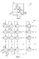
- Figure 1 illustrates a cellular communications receiver.
- Figure 2 shows a signal processing chain including a DFT channelizer.
- Figure 3 shows a block diagram of a resampling filter.
- Figure 4 shows the frequency response of a polyphase filter.
- Figure 5 shows a block diagram of a polyphase filter processing block.
- Figure 6 depicts an n/m oversampling polyphase filter constructed using the polyphase filter processing blocks.
- Figure 7 illustrates the frequency response of a raised cosine detection filter.
- Figure 8 shows a method for recovering individual communication channels from a received signal.
- the receiver may be, for example, a cellular communication base station.
- the receiver 100 includes an antenna 102, a downconverter 104, and a channelizer 106 (described in more detail below).
- the channelizer 106 provides the recovered channel outputs 108.
- the receiver 100 operates in a cellular communications system in which terminals transmit information in cellular communication channels assigned from a predetermined spectrum.
- the terminals may transmit information according to the European Global System Mobile (GSM) specification, that provides 200 KHz wide channels with 200 KHz spacing centered at 897.5 MHz and spanning 35 MHz of bandwidth.
- GSM European Global System Mobile
- the terminals may also transmit according to other types of standards, however, including the North American Interim Standard 54 or 136 standards.
- the downconverter 104 shifts a received signal to an intermediate frequency for further processing by the channelizer 106.
- the downconverter 104 may also be accompanied by additional functionality such as filtering, automatic gain control (e.g., between 0 and 36 dB), and analog to digital (A/D) conversion.
- the additional functionality may include, as examples, the equalization techniques described in TRW Docket No. 12-1214, titled “Intermediate Frequency Signal Amplitude Equalizer for Multichannel Applications", filed concurrently herewith, as serial no. , and TRW Docket No. 12-1215, titled “Amplitude Cancellation Topology for Multichannel Applications", filed concurrently herewith, as serial no. .
- the downconversion process may begin, for example, with a 15 MHz wide received signal on a 897.5 MHz center subsequently 14-bit sampled at 65 Msps.
- the downconversion process preferably provides an intermediate frequency of one-quarter of the A/D conversion sample rate, Fs, although three-quarters and one and one-quarter are also suitable.
- the intermediate frequency may be preferably offset by approximately 100 KHz.
- the processing chain includes a baseband converter 202, a resampling filter 204, and a polyphase filter 206.
- the processing chain further includes an n-point DFT circuit 208 providing the recovered channel outputs 210.
- a recovered channel output selection circuit 212 couples to the recovered channel outputs 210 and provides the selected channel outputs 214.
- n 130
- the 130-point DFT is performed as a set of 13-point DFTs followed by a set of 5-point DFTs followed by a set of 2-point DFTs. Performing the DFT using such a prime number factorization generally yields an implementation that requires less resources (e.g., gates, registers, memory, and the like).
- the processing chain 200 includes a raised cosine filter 216 coupled to a numeric format converter 214.
- a data formatter and buffer 220 and a communication interface 222 follow.
- the channelizer 224 may be regarded as the polyphase filter 206 followed by the n-point DFT circuit 208.
- the additional support circuitry 202-204 and 212-222 may be added as desired, or as required by a particular application.
- the baseband converter 202 provides digital mixers, oscillators, and other support circuitry that convert incoming digital samples of a received signal to complex baseband.
- the resultant Inphase (I) and Quadrature (Q) samples represent signal content centered around approximately DC.
- the received signal is preferably a wide slice (e.g., 15-35 MHz) of spectrum spanning multiple communication channels.
- the received signal may be 15 MHz wide, thereby spanning 75 200 KHz wide channels, with 200 KHz spacing.
- the received signal may be 15 MHz wide, thereby spanning 75 200 KHz wide channels, with 200 KHz spacing.
- only every third frequency is used.
- a 15 MHz portion of spectrum may in some instances include 25 active channels, rather than 75.
- the samples input to the baseband converter 202 are preferably 20 bit real samples.
- the baseband converter 202 may then downconvert by Fs/4 using a 35 tap low pass filter with approximately 0.0045 dB peak to peak pass band ripple and 91.8 dB stop band attenuation.
- the samples output from the baseband converter are 22 bit I and 22 bit Q samples at 65 Msps.
- a front end A/D converter provides received signal samples at a predetermined A/D converter sample rate.
- the n-point DFT 208 may be designed to accommodate a different sample rate, given the communication channel spacing, communication channel output sample rate, and number of communication channels that the DFT circuit 208 recovers simultaneously.
- the front end A/D converter sample rate is 65 Msps
- the preferred DFT circuit 208 sample rate is 26 Msps.
- the invention provides the resampling filter 204 to adapt the front end processing to the DFT processing.
- the front end processing and the DFT processing may thereby be designed with different goals in mind, and one need not be unduly limited by the other.
- the resampling filter 300 includes an interpolator 302, a low pass filter 304, and a decimator 306. An input data rate input 308 and an output data rate output 310 are also shown.
- the interpolator 302 and decimator 306 function as resampling circuitry to adapt an input data rate to an output data rate.
- additional interpolation or decimation may be used, and the interpolations and decimations may be by different amounts in order to provide a suitable output data rate given an input data rate.
- the interpolator 302 may provide an interpolation by 2
- the decimator 306 may provide a decimation by 5.
- the low pass filter may be a 16 tap finite impulse response filter with approximately 0.021 dB peak to peak pass band ripple and 96.23 dB stop band attenuation.
- the samples output from the resampling filter 204 are 22 bit I and 22 bit Q samples at 26 Msps.
- the output of the resampling filter 300 may be served by a dual port SRAM that receives samples from the resampling filter 300 and that provides samples to the polyphase filter 206.
- the dual port SRAM may be 24,992 bits in size.
- the output of the resampling filter 204 feeds the polyphase filter 206.
- a polyphase filter provides a set of filter structures in parallel, each of which may be selected at a different time to provide the different phases of the filter on incoming data.
- the DFT circuit 208 provides n outputs, each of which is a narrowband channelized communication signal with the same bandwidth but that originated a different center frequency.
- the polyphase filter 206 provides the desired frequency response for each of the n communication channels.
- the DFT circuit 208 then replicates the frequency response across all the center frequencies at the same time.
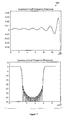
- Figure 4 presents a suitable frequency response 400 for the polyphase filter 206.
- the frequency response 400 provides peak to peak pass band ripple of approximately 0.023 dB and a minimum stop band attenuation of approximately 96.7 dB using a 520 tap digital low pass filter.
- the samples output from the polyphase filter 206 are preferably 22 bit I and 22 bit Q samples.
- the polyphase filter 206 preferably implements an oversampling ratio of n/m, where n and m are integers with m ⁇ n.
- FIG. 5 that figure illustrates a block diagram of a polyphase filter processing block 500.
- the processing block 500 includes a delay element (e.g., a memory) 502, a multiplier 504, and a summer 506.
- Each processing block 500 also stores a filter coefficient h(j).
- Signal samples enter the processing block on the sample input 508 and exit on the sample output 510.
- a partial sum input 512 connects to the summer 506, which, in turn provides the partial sum output 514.
- Each signal sample stored in the delay element 502 is multiplied against the filter coefficient h(j), and added to the sample value on the partial sum input 512.
- the resultant sum is output on the partial sum output 514.
- FIG. 6 depicts an oversampling polyphase filter 600 constructed using the polyphase filter processing blocks 500 (e.g., the processing blocks 602 and 604 shown labeled in Figure 6).
- Each processing block includes a sample input (e.g., the sample input 606), a sample output (e.g., the sample output 608), a partial sum input (e.g., the partial sum input 610), and a partial sum output (e.g., the partial sum output 612).
- Processing blocks in the first column are presented with a constant value (e.g., zero) on their partial sum inputs.
- Figure 6 also shows a filter input 614 and n filter outputs y(m).
- the polyphase filter 600 is arranged as n rows by k columns (i.e., a matrix of k*n processing blocks). Each processing block in the polyphase filter 600 stores or is otherwise associated with a filter coefficient h(j).
- the k*n filter coefficients h(j) implement the frequency response 400 illustrated in Figure 4.
- m samples shift into the polyphase filter 600 (the oldest m samples are discarded) on the filter input 614.
- the n outputs y 0 (m) through y n-1 (m) are computed.
- the polyphase filter 600 thus provides an oversampling ratio of n/m with a window length of k*n and a presum ratio of k:1.
- the polyphase filter 206 may be served by two single port SRAMs.
- the polyphase filter 206 writes to one SRAM while the DFT circuit 208 reads from the other.
- each SRAM may be 5720 bits (i.e., large enough to hold 130 22-bit I samples and 22-bit Q samples).
- the DFT circuit 208 operates on the polyphase filtered signal provided by the polyphase filter 206.
- the DFT circuit 208 implements an n-point DFT to provide n narrowband channelized communication signals individually on the recovered channel outputs 210.
- the DFT circuit 208 provides 130 individual outputs.
- the DFT circuit 208 is tailored to a particular cellular communication system, communication channel spacing, communication channel output sample rate, and number of communication channels.
- the communication channel spacing is 200 KHz
- the communication channel output sample rate may be a multiple of a symbol rate of a GSM communication signal
- the number of communication channels, N may be 75 (assuming processing of 15 MHz of spectrum).
- N/M 130/48, yielding a Fs_in of 26 MHz.
- the resampling filter 204 adapts the front end sample rate to be commensurate with the desired DFT circuit 208 sample rate.
- the DFT circuit 208 preferably outputs 28 bit I and 28 bit Q output samples, for example, at 1625/3 Ksps.
- the 130 point DFT may be performed first as a set of 13-point DFTs, followed by a set of 5-point DFTs, then a set of 2-point DFTs.
- a 6760 bit single port SRAM may be provided to store the results of the 13-point DFT.
- the recovered channel output selection circuit 212 determines which recovered channel signals to pass on for further processing. To that end, the selection circuit 212 may operate in response to a multibit control signal specifying the recovered channel signals to retain on the selected channel outputs 214. The remaining recovered channel signals are discarded.
- the control signal may, for example, control circuitry that selectively stores in memory or discards outputs of the DFT circuit 208, thereby selecting or retaining a subset of recovered channel signals.
- the output samples remain 28 bit I and 28 bit Q output samples at 1625/3 Ksps.
- the raised cosine filter 216 filters the subset of recovered channel signals that are retained. To that end, there may be multiple raised cosine filters 216 (e.g., one for each recovered channel signal).
- the raised cosine filter 216 provides, using a finite impulse response filter, a frequency response matched to the transmitter frequency response.
- An exemplary raised cosine filter frequency response 700 is shown in Figure 7.
- the raised cosine filter 216 may be implemented, for example, using a 49 tap finite impulse response filter with approximately 0.04 dB peak to peak pass band ripple.
- the output samples remain 28 bit I and 28 bit Q output samples at 1625/3 Ksps.
- the optional numeric format converter 218 provides circuitry that converts the numeric representation used by previous processing elements to a different numeric format (if any) desired for subsequent processing.
- the numeric format converter 218 is preferably implemented using discrete logic that converts the fixed point representation used in previous processing steps to a floating point representation with a mantissa and an exponent between 2 0 and 2 15 .
- the output samples are preferably 12 bit I and 12 bit Q samples with 4 bits of gain information, at 1625/3 Ksps.
- the data formatter and buffer 220 provides circuitry to arrange the samples, after numeric formatting, into a desired output format, and to buffer the samples for transmission. For example, the data formatter and buffer 220 may prepare the samples for transmission according to a predetermined communication standard. The output samples remain 12 bit I and 12 bit Q samples with 4 bits of gain information, at 1625/3 Ksps.
- the communication interface 222 provides a transport mechanism for transmitting the output samples to subsequent processing.
- the communication interface 222 may be a serial, parallel, or network interface.
- the processing chain 200 may be implemented in digital form in one or more ASICs.
- those outputs may, in fact, be blocks of memory rather than discrete signal connections.
- the output selection circuit 212 may pass or block certain recovered channel signals by writing to or clearing memory areas, rather than providing outputs on discrete signal connections.
- FIG. 8 that figure illustrates a method for recovering individual communication channels from a received signal.
- a transmitted signal is received (802).
- the transmitted signal spans multiple communication channels in bandwidth.
- the processing chain 200 digitizes (804) the transmitted signal to form a digitized input signal.
- the processing chain 200 resamples (806) the digitized received signal from an input data rate to an output data rate commensurate with a preselected communication channel spacing, communication channel output sample rate, and a number of communication channels.
- the processing chain 200 then performs (810) an n-point DFT on the polyphase filtered resampled signal to recover individual communication channels.
- the processing chain may then select (812) a subset of individual recovered channels to preserve for subsequent processing.
- the invention thereby provides a method and apparatus for recovering many communication channels simultaneously without the need to repeat, for example, individual sub-band tuners.
- the invention provides significant cost and complexity benefits that grow with the number of communications channels recovered.
- the invention further allows a channelizer to adapt, using a resampling filter, to a wide range of input sample rates.
Landscapes
- Engineering & Computer Science (AREA)
- Computer Networks & Wireless Communication (AREA)
- Signal Processing (AREA)
- Analogue/Digital Conversion (AREA)
- Transmission Systems Not Characterized By The Medium Used For Transmission (AREA)
- Circuits Of Receivers In General (AREA)
Applications Claiming Priority (2)
| Application Number | Priority Date | Filing Date | Title |
|---|---|---|---|
| US09/971,750 US20030069009A1 (en) | 2001-10-04 | 2001-10-04 | Cellular communications channelizer |
| US971750 | 2001-10-04 |
Publications (1)
| Publication Number | Publication Date |
|---|---|
| EP1300958A2 true EP1300958A2 (de) | 2003-04-09 |
Family
ID=25518758
Family Applications (1)
| Application Number | Title | Priority Date | Filing Date |
|---|---|---|---|
| EP02022463A Withdrawn EP1300958A2 (de) | 2001-10-04 | 2002-10-04 | Kanalformer für Zellular-Kommunikationen |
Country Status (3)
| Country | Link |
|---|---|
| US (1) | US20030069009A1 (de) |
| EP (1) | EP1300958A2 (de) |
| JP (1) | JP2003188840A (de) |
Cited By (3)
| Publication number | Priority date | Publication date | Assignee | Title |
|---|---|---|---|---|
| US20140269852A1 (en) * | 2013-03-13 | 2014-09-18 | Analog Devices Technology | Radio frequency transmitter noise cancellation |
| CN105227157A (zh) * | 2015-11-09 | 2016-01-06 | 天津理工大学 | 二维dft域全相位数字滤波器实现方法 |
| US9912358B2 (en) | 2015-03-20 | 2018-03-06 | Analog Devices Global | Method of and apparatus for transmit noise reduction at a receiver |
Families Citing this family (4)
| Publication number | Priority date | Publication date | Assignee | Title |
|---|---|---|---|---|
| US7158591B2 (en) * | 2001-05-09 | 2007-01-02 | Signum Concept, Inc. | Recursive resampling digital filter structure for demodulating 3G wireless signals |
| US7340024B1 (en) * | 2003-10-22 | 2008-03-04 | L3 Communications Corporation | Parallel fractional interpolator with data-rate clock synchronization |
| CA2825707A1 (en) | 2011-01-21 | 2012-07-26 | Tommy Yu | Systems and methods for selecting digital content channels using low noise block converters including digital channelizer switches |
| US10763906B1 (en) * | 2020-01-22 | 2020-09-01 | United States Of America As Represented By The Secretary Of The Navy | Cognitive radio technique for efficiently receiving multiple signals using polyphase downconverter channelizers |
Family Cites Families (8)
| Publication number | Priority date | Publication date | Assignee | Title |
|---|---|---|---|---|
| US5926455A (en) * | 1996-12-19 | 1999-07-20 | Lucent Technologies Inc. | Recursive filters for polyphase structures |
| US5999573A (en) * | 1997-08-29 | 1999-12-07 | Ericsson Inc. | Wideband channelization with variable sampling frequency |
| US6282184B1 (en) * | 1997-12-22 | 2001-08-28 | Nortel Networks Limited | Common digitizing rate for multiple air interfaces for generic cell sites in cellular radio |
| US6356569B1 (en) * | 1997-12-31 | 2002-03-12 | At&T Corp | Digital channelizer with arbitrary output sampling frequency |
| JP3805984B2 (ja) * | 1998-12-24 | 2006-08-09 | ノキア ネットワークス オサケ ユキチュア | 信号の増幅を減少させるための装置および方法 |
| US6985545B2 (en) * | 2000-12-26 | 2006-01-10 | Nortel Networks Limited | Apparatus and method to provide spectrum sharing for two or more RF signals occupying an overlapping RF bandwidth |
| US7164741B2 (en) * | 2001-05-09 | 2007-01-16 | Signum Concept, Inc. | Non-recursive resampling digital fir filter structure for demodulating 3G cellular signals |
| US7158591B2 (en) * | 2001-05-09 | 2007-01-02 | Signum Concept, Inc. | Recursive resampling digital filter structure for demodulating 3G wireless signals |
-
2001
- 2001-10-04 US US09/971,750 patent/US20030069009A1/en not_active Abandoned
-
2002
- 2002-10-04 EP EP02022463A patent/EP1300958A2/de not_active Withdrawn
- 2002-10-04 JP JP2002291901A patent/JP2003188840A/ja active Pending
Cited By (5)
| Publication number | Priority date | Publication date | Assignee | Title |
|---|---|---|---|---|
| US20140269852A1 (en) * | 2013-03-13 | 2014-09-18 | Analog Devices Technology | Radio frequency transmitter noise cancellation |
| US9831898B2 (en) * | 2013-03-13 | 2017-11-28 | Analog Devices Global | Radio frequency transmitter noise cancellation |
| US10644731B2 (en) | 2013-03-13 | 2020-05-05 | Analog Devices International Unlimited Company | Radio frequency transmitter noise cancellation |
| US9912358B2 (en) | 2015-03-20 | 2018-03-06 | Analog Devices Global | Method of and apparatus for transmit noise reduction at a receiver |
| CN105227157A (zh) * | 2015-11-09 | 2016-01-06 | 天津理工大学 | 二维dft域全相位数字滤波器实现方法 |
Also Published As
| Publication number | Publication date |
|---|---|
| US20030069009A1 (en) | 2003-04-10 |
| JP2003188840A (ja) | 2003-07-04 |
Similar Documents
| Publication | Publication Date | Title |
|---|---|---|
| EP1114516B1 (de) | Flexibilitätsverbesserung eines modifizierten schnellen faltungsalgoritmus | |
| USRE41797E1 (en) | Polyphase channelization system | |
| US8472562B2 (en) | Digital receiver and method | |
| CA2066540C (en) | Multiple user digital receiving apparatus and method with time division multiplexing | |
| US7596189B2 (en) | Quadrature receiver sampling architecture | |
| EP1086542B1 (de) | Verfahren und vorrichtung zur digitalen kanalisierung und dekanalisierung | |
| US20040152418A1 (en) | Unified digital front end for IEEE 802.11g WLAN system | |
| JP2001313545A (ja) | 広帯域通信用の重複及び加算フィルタ | |
| EP1451993B1 (de) | Digitaler multiratensender/-empfänger | |
| EP1300958A2 (de) | Kanalformer für Zellular-Kommunikationen | |
| AU692412B2 (en) | Method and apparatus for transmultiplexer a multi-channel information signal | |
| KR100432987B1 (ko) | 통신 단말기용 수신 회로 및 수신 회로에서의 신호 처리방법 | |
| JP2002271431A (ja) | 低域通過フィルタ | |
| US20030069022A1 (en) | Amplitude cancellation topology for multichannel applications | |
| KR20020034061A (ko) | 시디엠에이 시스템에서 병렬 처리 필터링 방법 및 그 장치 |
Legal Events
| Date | Code | Title | Description |
|---|---|---|---|
| PUAI | Public reference made under article 153(3) epc to a published international application that has entered the european phase |
Free format text: ORIGINAL CODE: 0009012 |
|
| AK | Designated contracting states |
Kind code of ref document: A2 Designated state(s): AT BE BG CH CY CZ DE DK EE ES FI FR GB GR IE IT LI LU MC NL PT SE SK TR Designated state(s): AT BE BG CH CY CZ DE DK EE ES FI FR GB GR IE IT LI LU MC NL PT SE SK TR |
|
| AX | Request for extension of the european patent |
Extension state: AL LT LV MK RO SI |
|
| RAP1 | Party data changed (applicant data changed or rights of an application transferred) |
Owner name: NORTHROP GRUMMAN CORPORATION |
|
| RAP1 | Party data changed (applicant data changed or rights of an application transferred) |
Owner name: NORTHROP GRUMMAN CORPORATION |
|
| STAA | Information on the status of an ep patent application or granted ep patent |
Free format text: STATUS: THE APPLICATION HAS BEEN WITHDRAWN |
|
| 18W | Application withdrawn |
Effective date: 20050629 |