EP1301823B1 - Dispositif a cristaux liquides - Google Patents
Dispositif a cristaux liquides Download PDFInfo
- Publication number
- EP1301823B1 EP1301823B1 EP01956649A EP01956649A EP1301823B1 EP 1301823 B1 EP1301823 B1 EP 1301823B1 EP 01956649 A EP01956649 A EP 01956649A EP 01956649 A EP01956649 A EP 01956649A EP 1301823 B1 EP1301823 B1 EP 1301823B1
- Authority
- EP
- European Patent Office
- Prior art keywords
- liquid crystal
- defect
- grating
- crystal device
- stable
- Prior art date
- Legal status (The legal status is an assumption and is not a legal conclusion. Google has not performed a legal analysis and makes no representation as to the accuracy of the status listed.)
- Expired - Lifetime
Links
- 0 CCC1*CCC1 Chemical compound CCC1*CCC1 0.000 description 5
Images




Classifications
-
- G—PHYSICS
- G02—OPTICS
- G02F—OPTICAL DEVICES OR ARRANGEMENTS FOR THE CONTROL OF LIGHT BY MODIFICATION OF THE OPTICAL PROPERTIES OF THE MEDIA OF THE ELEMENTS INVOLVED THEREIN; NON-LINEAR OPTICS; FREQUENCY-CHANGING OF LIGHT; OPTICAL LOGIC ELEMENTS; OPTICAL ANALOGUE/DIGITAL CONVERTERS
- G02F1/00—Devices or arrangements for the control of the intensity, colour, phase, polarisation or direction of light arriving from an independent light source, e.g. switching, gating or modulating; Non-linear optics
- G02F1/01—Devices or arrangements for the control of the intensity, colour, phase, polarisation or direction of light arriving from an independent light source, e.g. switching, gating or modulating; Non-linear optics for the control of the intensity, phase, polarisation or colour
- G02F1/13—Devices or arrangements for the control of the intensity, colour, phase, polarisation or direction of light arriving from an independent light source, e.g. switching, gating or modulating; Non-linear optics for the control of the intensity, phase, polarisation or colour based on liquid crystals, e.g. single liquid crystal display cells
- G02F1/137—Devices or arrangements for the control of the intensity, colour, phase, polarisation or direction of light arriving from an independent light source, e.g. switching, gating or modulating; Non-linear optics for the control of the intensity, phase, polarisation or colour based on liquid crystals, e.g. single liquid crystal display cells characterised by the electro-optical or magneto-optical effect, e.g. field-induced phase transition, orientation effect, guest-host interaction or dynamic scattering
- G02F1/139—Devices or arrangements for the control of the intensity, colour, phase, polarisation or direction of light arriving from an independent light source, e.g. switching, gating or modulating; Non-linear optics for the control of the intensity, phase, polarisation or colour based on liquid crystals, e.g. single liquid crystal display cells characterised by the electro-optical or magneto-optical effect, e.g. field-induced phase transition, orientation effect, guest-host interaction or dynamic scattering based on orientation effects in which the liquid crystal remains transparent
- G02F1/1391—Bistable or multi-stable liquid crystal cells
-
- G—PHYSICS
- G02—OPTICS
- G02F—OPTICAL DEVICES OR ARRANGEMENTS FOR THE CONTROL OF LIGHT BY MODIFICATION OF THE OPTICAL PROPERTIES OF THE MEDIA OF THE ELEMENTS INVOLVED THEREIN; NON-LINEAR OPTICS; FREQUENCY-CHANGING OF LIGHT; OPTICAL LOGIC ELEMENTS; OPTICAL ANALOGUE/DIGITAL CONVERTERS
- G02F1/00—Devices or arrangements for the control of the intensity, colour, phase, polarisation or direction of light arriving from an independent light source, e.g. switching, gating or modulating; Non-linear optics
- G02F1/01—Devices or arrangements for the control of the intensity, colour, phase, polarisation or direction of light arriving from an independent light source, e.g. switching, gating or modulating; Non-linear optics for the control of the intensity, phase, polarisation or colour
- G02F1/13—Devices or arrangements for the control of the intensity, colour, phase, polarisation or direction of light arriving from an independent light source, e.g. switching, gating or modulating; Non-linear optics for the control of the intensity, phase, polarisation or colour based on liquid crystals, e.g. single liquid crystal display cells
- G02F1/133—Constructional arrangements; Operation of liquid crystal cells; Circuit arrangements
- G02F1/1333—Constructional arrangements; Manufacturing methods
- G02F1/1337—Surface-induced orientation of the liquid crystal molecules, e.g. by alignment layers
-
- C—CHEMISTRY; METALLURGY
- C09—DYES; PAINTS; POLISHES; NATURAL RESINS; ADHESIVES; COMPOSITIONS NOT OTHERWISE PROVIDED FOR; APPLICATIONS OF MATERIALS NOT OTHERWISE PROVIDED FOR
- C09K—MATERIALS FOR MISCELLANEOUS APPLICATIONS, NOT PROVIDED FOR ELSEWHERE
- C09K2323/00—Functional layers of liquid crystal optical display excluding electroactive liquid crystal layer characterised by chemical composition
-
- C—CHEMISTRY; METALLURGY
- C09—DYES; PAINTS; POLISHES; NATURAL RESINS; ADHESIVES; COMPOSITIONS NOT OTHERWISE PROVIDED FOR; APPLICATIONS OF MATERIALS NOT OTHERWISE PROVIDED FOR
- C09K—MATERIALS FOR MISCELLANEOUS APPLICATIONS, NOT PROVIDED FOR ELSEWHERE
- C09K2323/00—Functional layers of liquid crystal optical display excluding electroactive liquid crystal layer characterised by chemical composition
- C09K2323/02—Alignment layer characterised by chemical composition
-
- G—PHYSICS
- G02—OPTICS
- G02F—OPTICAL DEVICES OR ARRANGEMENTS FOR THE CONTROL OF LIGHT BY MODIFICATION OF THE OPTICAL PROPERTIES OF THE MEDIA OF THE ELEMENTS INVOLVED THEREIN; NON-LINEAR OPTICS; FREQUENCY-CHANGING OF LIGHT; OPTICAL LOGIC ELEMENTS; OPTICAL ANALOGUE/DIGITAL CONVERTERS
- G02F1/00—Devices or arrangements for the control of the intensity, colour, phase, polarisation or direction of light arriving from an independent light source, e.g. switching, gating or modulating; Non-linear optics
- G02F1/01—Devices or arrangements for the control of the intensity, colour, phase, polarisation or direction of light arriving from an independent light source, e.g. switching, gating or modulating; Non-linear optics for the control of the intensity, phase, polarisation or colour
- G02F1/13—Devices or arrangements for the control of the intensity, colour, phase, polarisation or direction of light arriving from an independent light source, e.g. switching, gating or modulating; Non-linear optics for the control of the intensity, phase, polarisation or colour based on liquid crystals, e.g. single liquid crystal display cells
- G02F1/133—Constructional arrangements; Operation of liquid crystal cells; Circuit arrangements
- G02F1/1333—Constructional arrangements; Manufacturing methods
- G02F1/1337—Surface-induced orientation of the liquid crystal molecules, e.g. by alignment layers
- G02F1/133753—Surface-induced orientation of the liquid crystal molecules, e.g. by alignment layers with different alignment orientations or pretilt angles on a same surface, e.g. for grey scale or improved viewing angle
- G02F1/133761—Surface-induced orientation of the liquid crystal molecules, e.g. by alignment layers with different alignment orientations or pretilt angles on a same surface, e.g. for grey scale or improved viewing angle with different pretilt angles
-
- G—PHYSICS
- G02—OPTICS
- G02F—OPTICAL DEVICES OR ARRANGEMENTS FOR THE CONTROL OF LIGHT BY MODIFICATION OF THE OPTICAL PROPERTIES OF THE MEDIA OF THE ELEMENTS INVOLVED THEREIN; NON-LINEAR OPTICS; FREQUENCY-CHANGING OF LIGHT; OPTICAL LOGIC ELEMENTS; OPTICAL ANALOGUE/DIGITAL CONVERTERS
- G02F1/00—Devices or arrangements for the control of the intensity, colour, phase, polarisation or direction of light arriving from an independent light source, e.g. switching, gating or modulating; Non-linear optics
- G02F1/01—Devices or arrangements for the control of the intensity, colour, phase, polarisation or direction of light arriving from an independent light source, e.g. switching, gating or modulating; Non-linear optics for the control of the intensity, phase, polarisation or colour
- G02F1/13—Devices or arrangements for the control of the intensity, colour, phase, polarisation or direction of light arriving from an independent light source, e.g. switching, gating or modulating; Non-linear optics for the control of the intensity, phase, polarisation or colour based on liquid crystals, e.g. single liquid crystal display cells
- G02F1/133—Constructional arrangements; Operation of liquid crystal cells; Circuit arrangements
- G02F1/1333—Constructional arrangements; Manufacturing methods
- G02F1/1337—Surface-induced orientation of the liquid crystal molecules, e.g. by alignment layers
- G02F1/133776—Surface-induced orientation of the liquid crystal molecules, e.g. by alignment layers having structures locally influencing the alignment, e.g. unevenness
-
- G—PHYSICS
- G02—OPTICS
- G02F—OPTICAL DEVICES OR ARRANGEMENTS FOR THE CONTROL OF LIGHT BY MODIFICATION OF THE OPTICAL PROPERTIES OF THE MEDIA OF THE ELEMENTS INVOLVED THEREIN; NON-LINEAR OPTICS; FREQUENCY-CHANGING OF LIGHT; OPTICAL LOGIC ELEMENTS; OPTICAL ANALOGUE/DIGITAL CONVERTERS
- G02F2201/00—Constructional arrangements not provided for in groups G02F1/00 - G02F7/00
- G02F2201/30—Constructional arrangements not provided for in groups G02F1/00 - G02F7/00 grating
Definitions
- This invention relates to liquid crystal devices, in particular to nematic liquid crystal devices.
- Liquid crystal devices typically comprise a thin layer of a liquid crystal material contained between cell walls. Optically transparent electrode structures on the cell walls allow an electric field to be applied across the liquid crystal layer causing a re-ordering of the liquid crystal molecules.
- the liquid crystal device To produce displays with a larger number of addressable elements it is common to construct the liquid crystal device with a series of row electrodes on one wall and a series of column electrodes on the other wall. In this way a matrix of separately addressable elements or pixels is formed and a given voltage can be applied to each individual pixel in the device by applying certain voltages to given rows and columns.
- the technique of applying column and row voltage waveforms to switch each pixel of the display in turn is termed multiplexing.
- Twisted nematic (TN) liquid crystal devices are switched to an "on” state by application of a suitable voltage, and will switch back to an "off” state when the applied voltage falls below a certain level, i.e. these devices are monostable and loss of power leads to loss of the image.
- TN displays can be constructed using stripes of row and column electrodes on the upper and lower cell surfaces allowing the device to be multiplexed. The number of elements that can be addressed using rms methods is limited by the steepness of the device transmission vs voltage curve as detailed by Alt and Pleschko in IEEE Trans ED vol ED 21 1974 pages 146-155 .
- Active matrix TN devices have several advantages compared with rms addressed TN displays, including a relatively low operating voltage requirement and a wide temperature operating range. This allows construction of small and portable battery powered displays for applications such as laptop computers.
- bistable In addition to monostable liquid crystal devices of the type described above, devices are known where the liquid crystal can adopt two stable configurations, i.e. the device is bistable. In such a device it is possible to switch between the bistable states by applying a suitable electrical signal. After the suitable electrical signal has been applied, the liquid crystal switches into one of the two possible states and, until an electrical signal capable of switching the device into the alternative bistable state is applied, the device will remain in that state. If switching between bistable states occurs at a well defined voltage threshold, bistability also permits a high level of multiplexibility because, unlike monostable devices, there is no need to keep a certain rms voltage level across each switched pixel.
- CMOS complementary metal-oxide-semiconductor
- CMOS complementary metal-oxide-semiconductor
- a bistable display only needs to be updated when a new image is required.
- a bistable display might consume only 1/3600 of the power of a monostable display assuming similar operating voltages and cell spacing etc. This would allow battery size (and weight) to be significantly reduced.
- bistable liquid crystal displays include surface stabilised ferroelectric liquid crystal (SSFELC) devices as described by N A Clark and S T Lagerwall, Appl. Phys. Lett., 36, 11, 899 (1980 ). It has also been shown in Patent Applications WO 91/11747 (“Bistable electrochirally controlled liquid crystal optical device”) and WO 92/00546 (“Nematic liquid crystal display with surface bistability controlled by a flexoelectric effect”) that a nematic can be switched between two stable states via the use of chiral ions or flexoelectric coupling.
- SSFELC surface stabilised ferroelectric liquid crystal
- a zenithally bistable nematic device may be constructed using a grating of a given design such that the liquid crystal molecules can adopt two stable pretilt angles in the same azimuthal plane.
- the term "same azimuthal plane" is explained as follows: let the walls of a cell lie in the x, y plane, which means the normal to the cell walls is the z axis hence two pretilt angles in the same azimuthal plane means two different molecular positions in the same x, z plane.
- One of these states is a high pretilt state, whilst the other is a low pretilt state.
- the difference in energy between the states is minimised by altering the grating pitch and grating groove depth ratio for a grating of a given asymmetry, producing bistability over a range of grating conditions. This allows a device to be produced which can adopt either of two stable liquid crystal configurations. It is also demonstrated how a zero pretilt defect state, with an associated non-defect state, may be induced by a symmetrical sinusoidal grating surface.
- WO 99/34251 teaches another zenithally bistable device having a negative dielectric anisotropy material in a twisted nematic configuration.
- bistable displays will only exhibit two stable states.
- combinations of external polarisers for example, can be arranged so that one of the states produces a dark (or "off") state whilst the other states produces a light (or “on”) state.
- grey-scale in addition to the "dark” and “light” states. This is commonly achieved using either temporal or spatial dither, or some combination of both with bistable technologies such as surface stabilised ferroelectric devices.
- Temporal dither utilises variations of liquid crystal "dark” and "light” states for each pixel with time. Greyscale is achieved by switching each pixel "on” and “off' at a rate faster than the viewer can perceive. The average time the pixel is in the "light” state rather than the "dark” state determines the grey-level perceived. Temporal dither requires the liquid crystal to be switched at a faster rate, and therefore has disadvantages in that faster optical response times are required from the liquid crystal and the power consumption of the display is increased.
- Spatial dither is achieved by having each pixel comprising two or more sub-pixel regions. These sub-pixels can be of the same area or weighted with respect to each other and switching certain combinations of the sub-pixels to the "on” and “off” states gives the perception of an overall grey level (e.g. a level with intensity in-between that of the "on” and "off' states for the pixel).
- Spatial dither techniques require displays to be fabricated with a number of sub-pixel areas per pixel; this has the disadvantage of increased device fabrication complexity. Spatial dither also requires the use of separate electrical driving circuitry for each row and/or column of sub-pixels, adding to the overall complexity and cost of the electronics required to drive the device. In addition, spatial dither reduces the overall aperture ratio of the pixel, leading to a corresponding reduction in the maximum reflectivity or transmission associated with the device. The requirement to include separate row and/or column electrodes for the additional sub-pixels typically requires the electrode track width to be reduced, thereby increasing the electrical track resistance. This increases the power consumption of the display and can lead to nonuniformities of the display as the addressing signals change from one end of a line to the other.
- Analogue (or domain) greyscale is also known where partial, or incomplete, switching of domains within a pixel is used so that different grey-levels can be formed from varying the number and/or size of domains in the pixel. This has been used in ferroelectric liquid crystals and bistable cholesterics.
- each pixel is sub-divided into areas which respond differently to applied electric fields; for example by forming holes in the electrodes, including passive dielectric layers or inducing alignment variations etc.
- inducing multiple threshold is provided in Bryan-Brown et al, (1998) proceedings of Asia Display, p1051 - 1052 , where it is demonstrated that grey-scale may be achieved in a zenithally bistable device using a chirped grating that allows partial switching of an area of a pixel.
- US patent 4,333,708 describes how bistable nematic devices can be constructed using various surface boundary conditions.
- the bistability relies on the formation of defects at certain positions in various cell geometries and it is the cell itself that is bistable; not the individual cell surfaces.
- the different liquid crystal configurations are selected by applying certain combinations of voltages in the plane of the cell and perpendicular to the plane of the cell which causes reorientation of the bulk configurations of the liquid crystal.
- US patent 4,333,708 also describes how a plurality of bistable devices, each having a particular surface boundary conditions, can be combined in a single display to achieve grey-scale. Such a display would prove highly complex to manufacture.
- US5625477 describes how a cholesteric liquid crystal can form either a planar texture or a focal conic texture in an appropriate cell.
- the cholesteric pitch is chosen so that the planar texture reflects half the incident light, whilst the focal conic texture transmits all the light and leads to a black state if the sample back is blackened.
- Selection of the alignment state is controlled by the amplitude the applied voltage pulse, and it was shown that the relative proportions of domains adopting the planar or focal conic texture within a pixel area can be varied by applying voltage pulses of different durations. Disadvantages of this device include difficulties associated with obtaining greyscale and colour.
- a liquid crystal device capable of adopting at least two stable states comprises a layer of liquid crystal material located between two cell walls, a means of applying a voltage to the liquid crystal layer and a surface alignment grating on the internal surface of at least one cell wall wherein the surface profile of the surface alignment grating comprises three or more defect sites per grating period with at least one +1 ⁇ 2 defect site per grating period and at least one -1 ⁇ 2 defect site per grating period so that the liquid crystal molecules can adopt any one of two or more stable pretilt angles in the same azimuthal plane in the locality of the surface and wherein the arrangement is such that two or more stable liquid crystal molecular configurations can exist and wherein application of a suitable voltage causes the liquid crystal to adopt any one of two or more stable configurations.
- the liquid crystal molecules can adopt any one of three or more stable pretilt angles in the same azimuthal plane in the locality of the surface and wherein the arrangement is such that three or more stable liquid crystal molecular configurations can exist and wherein application of a suitable voltage causes the liquid crystal to adopt any one of three or more of the stable configurations.
- one pair of +1 ⁇ 2 and -1 ⁇ 2 defect sites are situated so as to impart a low surface pretilt for one defect state.
- This invention thus provides a liquid crystal device which can be switched between a plurality of different stable configurations. Therefore an inherent grey-scale capability is provided which overcomes the disadvantages associated with the spatial and temporal dither techniques described above. Furthermore, an additional advantage of this invention is that a low surface pretilt defect state can be formed which allows devices to be constructed that exhibit high optical contrast between the low surface pretilt defect state and any higher surface pretilt states. This device could also be used for phase modulation of light, for example it could be used as a Spatial Light Modulator.
- the low surface pretilt state is of a significantly lower energy than that of any of the other possible defect states, wherein only the non-defect state and the defect state of low pretilt can be readily selected on application of a voltage.
- this invention provides a bistable device with a difference in surface pretilt of substantially 90° between the low surface pretilt defect state and the high surface pretilt non-defect state, thereby providing optimum optical contrast between the two states. This has the advantage over the previous bistable device described in WO 97/14990 that a highly symmetrical grating is not required; the requirements for the grating design are that the defect sites are appropriately positioned.
- the surface alignment grating structure is treated with, or formed from, a material that induces a homeotropic alignment of the liquid crystal director with respect to the local surface direction.
- a material that induces a homeotropic alignment of the liquid crystal director with respect to the local surface direction is a material that induces a homeotropic alignment of the liquid crystal director with respect to the local surface direction.
- Various methods of inducing homeotropic alignment are well known.
- the surface alignment grating structure is treated with, or formed from, a material that induces a planar alignment of the liquid crystal director with respect to the local surface direction.
- a material that induces a planar alignment of the liquid crystal director with respect to the local surface direction is well known.
- one cell wall has a surface alignment grating structure and the other cell wall has a surface which induces homeotropic alignment of the liquid crystal or induces planar homogenous alignment of the liquid crystal.
- both cell walls may have surface alignment grating structures.
- the liquid crystal material may be a nematic liquid crystal material, in particular nematic liquid crystal material with a positive dielectric anisotropy. If the surface alignment grating structure is treated with, or formed from, a material that induces a planar alignment of the liquid crystal director with respect to the local surface direction a nematic liquid crystal material with a negative dielectric anisotropy is preferred.
- nematic liquid crystal is taken herein to include long pitch cholesteric materials.
- the pitch of the surface alignment grating structure is within the range of 0.1 ⁇ m to 10 ⁇ m. More preferably the pitch is greater than 500nm, more preferably the pitch is greater than 800nm and more preferably the pitch is greater than 1000nm. Furthermore, it is convenient for the pitch to be less than 5 ⁇ m and more convenient for the pitch to be less than 2 ⁇ m.
- the groove depth of the surface alignment grating structure is within the range of 0.05 ⁇ m to 3 ⁇ m and the two cell walls are separated by between 1 ⁇ m to 20 ⁇ m.
- a means of applying a plurality of voltages to the liquid crystal layer comprises a layer of electrically conductive, and substantially optically transparent, material applied to the internal surface of both cell walls. Furthermore the layers of electrically conductive material applied to the internal surface of both cell walls may be patterned so as to produce an array (or matrix) of addressable pixels.
- the electronics required to pass suitable electrical signals to an array of addressable pixels i.e. multiplexing a matrix device would be well known to a person skilled in the art.
- the liquid crystal device further comprising a means for optically distinguishing between at least two of the stable liquid crystal configurations adopted.
- the means for optically distinguishing between at least two of the liquid crystal configurations may comprise a pair of polarisers placed one either side of the liquid crystal device with their respective optic axes aligned with respect to the liquid crystal device such that the amount of light transmitted through the liquid crystal display will differ depending on which liquid crystal configuration is adopted, an optically reflective layer placed one side of the liquid crystal device and a polariser placed the other side of the liquid crystal device with its optic axis aligned with respect to the liquid crystal device such that the amount of light reflected by the device will differ depending on which liquid crystal configuration is adopted, or a dichroic dye, the dye being added to the liquid crystal such that the amount of light absorbed by the liquid crystal display will differ depending on which liquid crystal configuration is adopted.
- a multi-stable liquid crystal device comprises a layer of liquid crystal material located between two cell walls and a means of applying a voltage to the liquid crystal material wherein a surface alignment grating structure on the internal surface of at least one cell wall has a surface profile which is such so as to induce the liquid crystal molecules to adopt any of three or more stable pretilt angles in the same azimuthal plane and wherein the arrangement is such that three or more stable liquid crystal molecular configurations can exist and wherein application of a suitable voltage causes the liquid crystal material to adopt any one of three or more stable configurations.
- three different pretilt angles in the same azimuthal plane can be adopted.
- a bistable liquid crystal device comprises a layer of liquid crystal material located between two cell walls, a means of applying a voltage to the liquid crystal layer and a surface alignment grating on the internal surface of at least one cell wall wherein the surface profile of the surface alignment grating comprises three or more defect sites per grating period with at least one +1 ⁇ 2 defect site per grating period and at least one -1 ⁇ 2 defect site per grating period wherein one pair of +1 ⁇ 2 and -1 ⁇ 2 defect sites are situated so as to impart low surface pretilt in the azimuthal plane to one defect state wherein such low pretilt state is of a significantly lower energy than that of any of the other possible defect states wherein only the non-defect state and the defect state of low surface pretilt can be readily selected on application of a voltage.
- Low surface pretilt can be considered to be lower than 20°, preferably
- a description of the zenithal bistable device of WO 97/14990 will be given with reference to figures 1 and 2 wherein a liquid crystal layer (1) is in contact with an asymmetric surface alignment grating (1) of pitch W and groove depth h.
- the liquid crystal director is denoted by the vector n.
- the contour lines (3) are perpendicular to orientation of the liquid crystal director (n) and the grating surface has been treated, for example by coating with a homeotropic surfactant (not shown), to induce local homeotropic alignment of the liquid crystal at the interface (4) between the liquid crystal layer (2) and the surface alignment grating (1).
- homeotropic takes the meaning, well known to a person skilled in the art,' that the director (n) is oriented substantially perpendicularly to the local surface and herein a surface alignment grating is taken to mean an array of repeating elements of a unit length, as would be understood by a person skilled in the art.
- a surface alignment grating is taken to mean an array of repeating elements of a unit length, as would be understood by a person skilled in the art.
- the term “same azimuthal plane” is explained as follows: let the walls of a cell lie in the x, z plane, which means the normal to the cell walls is the y axis. Two pretilt angle in the same azimuthal plane means two different molecular positions in the same x, y plane.
- pretilt shall mean the tilt of the director away from the x-z plane at some distance away from the surface where the director is invariant in the x-z plane; hence perfectly planar alignment gives zero pretilt and perfectly homeotropic alignment gives 90° pretilt.
- a nematic liquid crystal in contact with an alignment grating surface coated with a homeotropic surfactant can adopt either a non-defect ( figure 1a ) or defect ( figure 1b ) alignment configuration.
- Liquid crystal defects can, in simple terms, be considered as a local area of discontinuity in the director field and are well known to persons skilled in the art.
- a summary of the theory relating to liquid crystal defects and disclinations can be found in P. G. deGennes, "The physics of liquid crystals" (Clarendon press, 1974).
- the nematic liquid crystal will, at the interface (4) between the surface alignment grating (1) and the liquid crystal (3), orient so as to be substantially perpendicular to the local surface of the grating (1).
- the liquid crystal will adopt a homeotropic alignment configuration of ⁇ p ⁇ 90°.
- defects of strength of approximately -1 ⁇ 2 (within a range of -1 to 0) and +1 ⁇ 2 (within a range of 0 to 1) are termed the "-1 ⁇ 2 defect” and the "+1 ⁇ 2 defect” respectively.
- the positions on a grating surface where +1 ⁇ 2 and -1 ⁇ 2 defects form are associated with regions of convex and concave minimum radii of curvature of the grating surface.
- the terms "-1 ⁇ 2 defect site” and "+1 ⁇ 2 defect site”, are taken to mean the region on a grating surface where a person skilled in the art would reasonably expect either a -1 ⁇ 2 or +1 ⁇ 2 defect to form using common general knowledge, documents such as P. G.
- defect site means either a -1 ⁇ 2 defect site or a +1 ⁇ 2 defect site and "defect sites” is simply more than one such defect site.
- FIG. 2 A suitable cell configuration to exploit the existence of the bistable surface described with respect to figure 1 , is shown in cross section in a stylised form in figure 2 .
- the cell configuration of figure 2 comprises a layer of nematic liquid crystal material with a positive dielectric anisotropy (2) sandwiched between a first glass wall (9) and a second glass wall (10).
- the first glass cell wall (10) is treated, for example by coating with lecithin (not shown), to induce homeotropic alignment of the nematic liquid crystal at the glass cell wall and liquid crystal interface (11).
- the second glass cell wall (10) is coated with a bistable surface alignment grating (1), the profile of which is as described with respect to figure 1 .
- the device of figure 2 allows the liquid crystal molecules to adopt either of two stable configurations, as shown in figures 2a and 2b .
- FIG 2a homeotropic alignment of the liquid crystal is induced at the first substantially flat cell wall surface (9) because of the homeotropic treatment (not shown).
- the liquid crystal (2) adopts a non-defect state (as described with respect to figure 1a ) and induces homeotropic alignment of the liquid crystal (2) within a short distance, with respect to the overall thickness of the liquid crystal cell (d), of the grating-liquid crystal interface (4).
- a uniform homeotropic (high tilt) alignment of the liquid crystal is obtained throughout the bulk of the cell.
- the pretilt associated with a particular pair of +1 ⁇ 2 and -1 ⁇ 2 defects has been found to depend on the relative positions of the +1 ⁇ 2 and -1 ⁇ 2 defects per grating period.
- a model of the pretilt induced at a surface by a grating structure will now be described with reference to figures 1 to 3 .
- the static director field is governed by a torque balance equation obtained from minimising the Frank-Oseen free energy of a nematic liquid crystal.
- a torque balance equation obtained from minimising the Frank-Oseen free energy of a nematic liquid crystal.
- G the Frank-Oseen free energy per unit length
- K is the bend or splay elastic constant.
- the torque balance equation 2 is simply the Laplace equation.
- any analytic function is a solution to the Laplace equation.
- the problem is directly analogous to the potential flow fluid mechanics or two dimensional electrostatics; see for example M. R. Speigel, “theory and problems of complex variables” (Schaum, New York, 1964 ) and P. M. Morse and H. Feshbach, “Methods of theoretical physics” (McGraw-Hill, New York, 1953 ).
- the equivalents of the disclination lines are the line sources or sinks in potential flow fluid mechanics and line charges in two dimensional electrostatics.
- Equation 3 is a generalisation of the case of a pair of disclination lines as described in, for example, P. G. deGennes & J Prost, "The physics of liquid crystals” (Academic, New York, 1993 ).
- the integral in equation 10 is obtained by an integration by parts technique. The integral is performed along a cut from (a n ,b n ) in the direction of (a n ,b n ) - (a n ',b n '). Along the cut, ⁇ n goes through a discontinuous change of 2 ⁇ M n as one traverses across the cut in the anti-clockwise direction. Evaluated the integral 10 yields equation 11 for the free energy. As noted in P. M. Chaikin & T. C. Lubensky, “Principles of condensed matter physics” (Cambridge University Press, 1995 ), the InR divergence in part of equation 11 can be eliminated if the sum of the strengths of all disclination lines in the system is zero
- Equation 15 was obtained from equation 14 by using the infinite products expansion of the sine function as in, for example, P. M. Morse and H. Feshbach, "Methods of theoretical physics" (McGraw-Hill, New York, 1953 ).
- the alignment grating will induce a finite surface tilt.
- +1 ⁇ 2 defects will form at the +1 ⁇ 2 defect sites (21) and -1 ⁇ 2 defects will form at the -1 ⁇ 2 defect sites (22) and the surface alignment grating will impart a pretilt to the liquid crystal, within a short distance of the surface compared to the overall cell thickness, according to equation 17.
- ⁇ is the harmonic conjugate of ⁇ and a is the radius of the defect line core measured in w .
- the first square bracket term of equation 19 is the nematic deformation energy without any defect.
- the middle square bracket term of equation 19 is due to the coupling of the defect and non-defect deformation.
- the last term of equation 19 depends only on the defects. With g , the energetic stability of the defect can be analysed with respect to the variation of ⁇ ⁇ and m .
- g K 2 ⁇ L ⁇ ⁇ ⁇ g 0 + g od + g dd
- ⁇ is the electrostatic potential.
- ⁇ and ⁇ can be understood as the analogues of the electric field intensity and potential in electrostatics.
- the lines of constants ⁇ and ⁇ are orthogonal as electric lines and equipotentials are normal to one another.
- the mathematical meaning of ⁇ is the natural logarithm of the Jacobian for the conformal transformation w ⁇ z , as described by M. R Speigal, "Complex Variables", Schaum's outline series, McGraw Hill, 1974 .
- ⁇ measures in the logarithmic scale, the magnitude of the rate of change of z with respect to the rate of change of w .
- ⁇ 0 measures, in logarithmic scale, the ratio of an elemental area, ⁇ z, at z to its corresponding area, ⁇ w , at w ( z ) under a conformal transformation z ⁇ w .
- ⁇ 0 evaluated at the concave parts of a surface is bigger than ⁇ 0 at the convex parts of the surface.
- Figure 4 shows the conformal co-ordinates graphically; the bold lines (24) are the constant v 's and the normal lines (25) are the constant u 's; points a (26), b (28) and c (30) represent the flat, convex and concave curvatures; ⁇ 0 associate with these points are ordered as ⁇ 0 ( c ) > ⁇ 0 ( a ) > ⁇ 0 ( b )
- Equation 38 The second summation in equation 38 is always positive.
- the condition for the possibilities of multi-stable states is given by: ⁇ ⁇ N m ⁇ ⁇ ⁇ ⁇ ⁇ + ⁇ ⁇ , ⁇ N m ⁇ ⁇ m ⁇ ln ⁇ sin 2 ⁇ ⁇ ⁇ - ⁇ ⁇ 2 ⁇ 0 for some configuration disclination lines on the grating position at ⁇ ⁇ 's.
- Figure 5 shows a series of gratings and a representation of a cross-section through the energy profile.
- the energy profile is obtained as a function of both -1 ⁇ 2 defect position and +1 ⁇ 2 defect position on the grating, producing a three dimensional energy profile.
- Figures 5b, 5d, and 5f show a cross section of this profile (in each case the same profile).
- Figure 5a represents a symmetrical sinusoidal grating. It can be seen that two energy minima occur (30, 31).
- the first energy minimum (30) is associated with coincident - 1 ⁇ 2 and +1 ⁇ 2 defect positions (i.e. the non-defect state) has a calculated pretilt of 90°.
- the second energy minimum (31) is associated with the +1 ⁇ 2 defect being at the convex defect site and the -1 ⁇ 2 defect being at the concave defect site; this gives a pretilt of 0°.
- Figure 5c represents an asymmetric sinusoidal grating. It can be seen that two energy minima occur (33, 34).
- the first energy minimum (33) is associated with coincident - 1 ⁇ 2 and +1 ⁇ 2 defect positions (i.e. the non-defect state) has a calculated pretilt of 90°.
- the second energy minimum (34) is associated with the +1 ⁇ 2 defect being at the convex defect site and the -1 ⁇ 2 defect being at the concave defect site; this gives a pretilt of 36°.
- Figure 5e represents an asymmetric square grating with four defect sites. It can be seen that five energy minima occur (35, 36, 37, 38, 39).
- the energy minimum (37) is associated with coincident -1 ⁇ 2 and +1 ⁇ 2 defect positions (i.e. the non-defect state) has a calculated pretilt of 90°.
- the other four energy minima (35, 36, 38, 39) are associated with the various combinations of +1 ⁇ 2 defect and -1 ⁇ 2 defect positions as described with reference to 7.
- the energy minimum (39) gives a pretilt of 0°.
- a computer implementation of the above model allows the surface pretilt induced by a surface alignment grating, and the energy associated with that particular configuration, to be calculated from a particular defect pair position on a given surface alignment grating profile.
- the model described above with reference to figures 4 and 5 demonstrates that for a given surface profile it is possible to obtain a plurality of stable surface states, and allows the pretilt associated with such states to be calculated. Such multi-stability is found within one period of the grating when there are three or more defect sites and at least one defect site has a maximum curvature which is convex and at least one defect site has a maximum radius of curvature which is concave.
- a plurality of defect sites per unit length of grating allows the formation of defect pairs at a plurality of positions within a single grating period. It is only possible for -1 ⁇ 2 and -1 ⁇ 2 defects to form in pairs; a single defect, or two -1 ⁇ 2 defects, can not form alone. Each +1 ⁇ 2 and -1 ⁇ 2 defect pair position induces a liquid crystal pretilt that could be calculated rigorously using the model described with reference to figures 4 and 5 above, or less rigorously using the simple model described with reference to figures 1 to 3 above.
- a plurality of defect sites per grating period, the formation of defect pair combinations and the pretilt associated with the various defect site configurations will now be described with reference to figures 6 to 9 .
- Figure 6 depicts a surface alignment grating (40) with a single +1 ⁇ 2 defect site (42) per grating period, L.
- the surface alignment grating has two possible -1 ⁇ 2 defect sites per grating period; a first -1 ⁇ 2 defect site (44) and a second -1 ⁇ 2 defect site (46).
- Two possible defect states could then be formed with a +1 ⁇ 2 defect at the +1 ⁇ 2 defect site (42) and a -1 ⁇ 2 defect at either the first -1 ⁇ 2 defect site (44) or the second -1 ⁇ 2 defect site (46).
- FIG. 6b depicts a surface alignment grating (40) with a single +1 ⁇ 2 defect site (42) per grating period, L.
- the surface alignment grating has two possible -1 ⁇ 2 defect sites per grating period; a first -1 ⁇ 2 defect site (44) and a second -1 ⁇ 2 defect site (46).
- Two possible defect states could then be formed with a +1 ⁇ 2 defect at the +1 ⁇ 2 defect site (42)
- a non-defect configuration can also be adopted by the nematic liquid crystal at the grating surface.
- the surface alignment grating of figure 6 thus provides three (two defect and a non-defect) stable surface pretilt configurations.
- Liquid crystal (2) in contact with the surface alignment grating (52) could adopt any one of four possible defect configurations, as shown in figures 7a, 7b, 7c and 7d .
- the defect pair configurations shown in figures 7a, 7b, 7c and 7d will induce surface pretilts of ⁇ 1 , ⁇ 2 , ⁇ 3 and ⁇ 4 respectively.
- the surface pretilt angles ⁇ 1 , ⁇ 2, ⁇ 3 and ⁇ 4 can be estimated using equation 17 from the ratios of distances d 1 , d 2 , d 3 , d 4 to L.
- the surface pretilt angles ⁇ 1 and ⁇ 2 occupy angles which are complimentary, and are therefore symmetric about the substrate normal. The same is true for ⁇ 3 and ⁇ 4 .
- the ⁇ 1 and ⁇ 2 states have the lower energy configuration since the high average surface tilt possessed by ⁇ 3 and ⁇ 4 can be more readily attained by adopting the non-defect high tilt configuration.
- Equivalent but opposite pretilts may also have advantages, such as wider viewing angle (similar to dual domain TN).
- zero pretilt is imparted to the liquid crystal (2) by the surface alignment grating (62) if a -1 ⁇ 2 defect forms at the second -1 ⁇ 2 defect site (66) and a +1 ⁇ 2 defect forms at the second +1 ⁇ 2 defect site (70).
- the two other possible combinations of the -1 ⁇ 2 and +1 ⁇ 2 defect position will impart a non-zero surface pretilt to the liquid crystal layer (2) according to equation 17.
- Each of the five possible states that may form on the symmetric alignment grating of figure 8a , or the asymmetric grating of figure 8b , will induce a certain liquid crystal surface pretilt angle and will have correspondingly different energies.
- the lower energy configurations will be those which induce the lower pretilt angles. If an asymmetric grating was so profiled, with an appropriate groove depth and pitch, the energy of one or more of the defect states could be made such that those defect states are less energetically favourable than the non-defect state and some or all of the other defect states.
- Surface grating structures can be designed, using the models and examples described above, where the defect sites are positioned so as to induce a plurality of states of various different energies, and/or where the surface pretilt of one or more of the defect states is to be controlled (for example to get defect states which induces substantially zero pretilt).
- FIG. 9 shows an alignment grating (82) with four -1 ⁇ 2 defect sites (84, 86, 88, 90) per unit length and four +1 ⁇ 2 defect sites (92, 94, 96, 98) per unit length.
- the alignment grating structure (82) would enable sixteen defect state configurations to be formed. No more than one pair of defect can form a defect state on this surface; to do so requires alternating +1 ⁇ 2 and -1 ⁇ 2 defect sites.
- the surface pretilt imparted to the liquid crystal by each of the defect states is defined by equation 17, and could also be calculated using the more rigorous model described above with reference to figures 4 and 5 . ,
- Surface alignment gratings may be profiled so as to favour the formation of more than one pair of +1 ⁇ 2 and -1 ⁇ 2 defects per unit length of grating, by producing structures with alternating +1 ⁇ 2 and -1 ⁇ 2 defect sites.
- FIG. 10 An example of a surface alignment grating, profiled so as to favour the formation of more than one pair of +1 ⁇ 2 and -1 ⁇ 2 defects per unit length of grating, will now be described with reference to figure 10 .
- the alignment imparted to a nematic liquid crystal layer by the type of grating structures described with reference to figure 10 will then be described with reference to figures 11 to 12 .
- p 2 >p 1 .
- Figure 10c shows a surface alignment grating (103) profiled such that one period p of the grooved surface is made up of one sub-period of the function fn1 (x) with pitch p/2 and amplitude A 1 plus one sub-period of the function fn1 (x) with pitch p/2 and amplitude A 2 .
- Figure 10d shows a surface alignment grating (120) profiled such that one period p of the grooved surface is, made up of one period of the function fn1 (x) with pitch p 1 and amplitude A 1 plus one period of the function fn1 (x) with pitch p 2 and amplitude A 2 .
- the surface alignment grating structure (102) given in figure 10b when in contact with a nematic liquid crystal (2) is depicted in figure 11 .
- the nematic liquid crystal director, n is perpendicular to the iso-contour lines (101). From figure 11 , it can be seen that the surface alignment grating structure (102) has a first (104) and second (106) +1 ⁇ 2 defect site and a first (108) and second (110) -1 ⁇ 2 defect site.
- a non-defect, homeotropic, state is depicted in figure 11a .
- a +1 ⁇ 2 defect (112) forms at the first +1 ⁇ 2 defect site (104) and a -1 ⁇ 2 defect (114) forms at the first -1 ⁇ 2 defect site (108), giving an intermediate pretilt state governed by the relative position of the defect pair according to equation 17 as described above.
- a +1 ⁇ 2 defect (112) forms at the first +1 ⁇ 2 defect site (104) and a -1 ⁇ 2 defect (114) forms at the first -1 ⁇ 2 defect site (108) and in addition a second +1 ⁇ 2 defect (116) forms at the second +1 ⁇ 2 defect site (106) and a second -1 ⁇ 2 defect (118) forms at second -1 ⁇ 2 defect site (110).
- the formation of the two defect pairs per unit length of grating will produce a low surface pretilt state wherein the pretilt adopted by the liquid crystal a short distance, compared with the cell gap, from the grating surface (102) will be the average of that expected (from equation 17 above) for the defect states of a grating of pitch p 1 and a grating of pitch p 2 .
- the different grating profiles of the portion of the grating of pitch p 1 and the portion of the grating of pitch p 2 causes the first and second defect pairs to have different energies associated with their formation.
- the energy associated with a defect pair on a grating surface can be calculated using the detailed model of grating induced surface pretilt described above with reference to figures 4 and 5 .
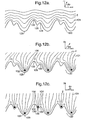
- the surface alignment grating structure (120) given in figure 10d when in contact with a nematic liquid crystal (2) is depicted in figure 12 .
- the surface alignment grating (120) has a first (122) and second (124) +1 ⁇ 2 defect site and a first (126) and second (128) -1 ⁇ 2 defect site.
- a non-defect, homeotropic, state is depicted in figure 12a .
- a defect state is shown where a first +1 ⁇ 2 defect (130) forms at the first +1 ⁇ 2 defect site (122) and a first -1 ⁇ 2 defect (132) forms at the first -1 ⁇ 2 defect site (126), giving an intermediate pretilt state governed by the relative position of the defect pair according to equation 17 as described above.
- Figure 12c depicts a defect state wherein two defect pairs have formed; a first +1 ⁇ 2 defect (130) at the first +1 ⁇ 2 defect site (122), a first -1 ⁇ 2 defect (132) at the first -1 ⁇ 2 defect site (126), a second +1 ⁇ 2 defect (134) at the second +1 ⁇ 2 defect site (124) and a second -1 ⁇ 2 defect (136) at the second -1 ⁇ 2 defect site (128).
- the pretilt associated with the defect state of figure 12b is governed by equation 17 whereas the pretilt associated with the defect pair state of figure 12c can be calculated by determining the average pretilt of two gratings of pitches p 1 and p 2 .
- the energy associated with each defect pair can, as described with reference to figure 11 above, be determined using the model described herein with reference to figure 4 and 5 .
- the surface alignment grating of period P described with reference to figure 12 above contains two distinct sub-period regions.
- the difference in defect energy associated with each of the sub-periods means that it is possible for stable states to form with no defects, one defect pair or two defect pairs. Each of these states will produce a different surface pretilt, allowing a tri-stable device to be readily constructed from such a surface alignment grating
- a grating consist of a number of sub-periods. It is also possible for each sub-period to possess more than two defects sites, thereby combining the structures described in figures 6 to 9 in the manner described with respect to figures 10 to 12 .
- a surface alignment grating which imparts three or more stable pretilt angles in the same azimuthal plane to the liquid crystal in the vicinity of the surface
- the overall grating period p to be less that half of the gap between the upper and lower cell walls. If the overall pitch p is more than approximately half the cell gap, defect pairs associated with adjacent sub-unit grating periods contained within the overall grating period will induce a surface pretilt that does not, in the vicinity of the surface, combine so as to form a plurality of stable pretilt angles in the same azimuthal plane.
- the surface pretilt associated with each defect pair would not merge within a short distance of the surface but would produce two distinct and adjacent regions of different bulk liquid crystal configuration (i.e. a striped texture when observed optically).
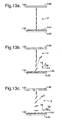
- the cell is constructed from two cell walls (140,142), where the first cell wall (142) has a multi-stable surface alignment grating (144) formed on its internal surface, in this example a tri-stable surface alignment grating in accordance with the teaching described above, whilst the second cell wall (142) has is treated so as to induce hometropic alignment to the nematic liquid crystal (2).
- the first (142) and second (140) cell walls are maintained typically 1-10 ⁇ m apart by a spacer ring (not shown), numerous beads of the same dimension dispersed within the liquid crystal (not shown) or numerous beads of the same dimension dispersed within any glue used to bond the cell walls together (not shown). Many other techniques of maintaining a gap between the cell walls are readily known to a person skilled in the art.
- a nematic liquid crystal (2) sandwiched between the first (142) and second (140) cell walls of can exist in any of three stable configurations; the non-defect configuration shown in figure 13(a) , the defect configuration shown in figure 13(b) or the defect configuration shown in figure 13(c) .
- the two defect state configurations of figures 13(a) and 13(b) arising from two possible positions which the bend defect can adopt on a the tri-stable surface alignment grating (144).
- a splay or bend deformation will lead to a macroscopic flexoelectric polarisation which is represented by the vector P in figure 13(b) and P' in figure 13(c) .
- a dc pulse applied to the electrodes (146) can couple to this flexoelectric polarisation, which is predominantly close to the alignment surface, and depending on its sign and magnitude any one of the three configurations can be selected.
- the cell configuration used to exploit the existence of a tri-stable surface alignment grating will also allow multi-stable surface alignment gratings to be exploited as multi-stable devices.
- the cell configurations described above can be combined with external polariser(s) and/or a reflector and the device may be operated in either transmissive or reflective mode.
- a dichroic dye may be mixed with the liquid crystal to get different absorption of light in the various multi-stable configurations. All these techniques of producing optical contrast from liquid crystal cell configuration are well known to a person skilled in the art.
- Optical compensation techniques may also be employed to enhance the optical contrast and viewing angle characteristics of any of the plurality of defect states.
- nematic material with positive, negative or zero dielectric anisotropy may be used in the cell configuration.
- Dual frequency nematic materials where the sign of dielectric anisotropy changes with the frequency of applied voltage, may also be used.
- a high positive dielectric anisotropy, and associated high flexoelectric coefficient may be used.
- Super-twist nematic and active matrix nematic materials would be suitable, although there is no requirement for the high ionic purity of liquid crystal required for the operation of active matrix devices.
- the cell walls may be formed of a relatively thick non flexible material such as a glass, or one or both walls may be formed of a flexible material such as a thin layer of glass or a plastic flexible material e.g. polyolefin or polypropylene.
- a plastic cell wall may be embossed on its inner surface to provide a grating. Additionally, the embossing may provide small pillars (e.g. of 1-10 ⁇ m height and 5-50 ⁇ m or more width) for assisting in correct spacing apart of the cell walls and also for a barrier to liquid crystal material flow when the cell is flexed. Alternatively the pillars may be formed by the material of the alignment layers.
- the grating may be a profiled layer of a photopolymer formed by a photolithographic process e.g. M C Huntly, Diffraction Gratings (Academic Press, London, 1982) p 95-125 ; and F Horn, Physics World, 33 (March 1993 ).
- the grating may be formed by embossing; M T Gale, J Kane and K Knop, J App. Photo Eng, 4, 2, 41 (1978 ), or ruling; E G Loewen and R S Wiley, Proc SPIE, 88 (1987 ), or by transfer from a carrier layer.
- a grating of 0.2 ⁇ m to 5 ⁇ m pitch, with a groove depth of between 0.1 ⁇ m to 3 ⁇ m is preferred.
- a solution comprising 4 parts 1813 Shipley photoresist to one part PGMEA thinners was spun onto an Indium Tin Oxide (ITO) coated substrate producing a photoresist film thickness of approximately 0.8 ⁇ m.
- ITO Indium Tin Oxide
- Holographic interference of two beams was used to create a grating of 500nm pitch with a profile very close to being sinusoidal.
- the substrate was then developed to reveal the grating structure which was then hardened by exposure to light from a high intensity 254nm light source, followed by a hard-bake at 180°C which rendered the grating insoluble in liquid crystal material.
- the grating used for the experiment above was analysed, after performing the above experiments, using cross-sectional SEM and the grating profile is shown in figure 14 .
- the grating was treated with a homeotropic surfactant and assembled into a 10 ⁇ m cell opposite a planar anchoring grating which had been made by photolithography. After filling with liquid crystal and cooling into the nematic phase, only one state was observed. No degeneracy was present in this cell which immediately suggests a pretilt of zero. The pretilt of the bistable grating surface was measured, using the rotating crystal method to be 0.2°.
- a solution comprising 4 parts 1813 Shipley photoresist to one part PGMEA thinners was spun onto an ITO coated substrate producing a photoresist film thickness of approximately 0.8 ⁇ m.
- a 1 ⁇ m pitch chrome-on-glass master-grating was bolted down so that it sat in intimate contact with the photoresist coated substrate.
- the assembly was exposed at normal incidence to a well-collimated beam of light from a high power mercury lamp.
- a variable neutral density filter was put between the light source and the master grating so that a variable exposure was made in the direction of the grating grooves.
- the substrate was then unclamped and developed to reveal a grating structure which was then hardened by exposure to light from an high intensity 254nm source, followed by a hard-bake at 180°C which rendered the grating insoluble in liquid crystal material.
- a homeotropic surface treatment was applied.
- a grating made in this way which exhibited similar tilt angles in the low tilt configuration was snapped along the direction perpendicular to the grating grooves and characterised using SEM.
- the resulting photograph shown in figure 15 is a cross section of the grating profile.
- This symmetrical grating with normal boundary conditions was assembled opposite a second symmetrical grating which had been made using an identical method, but which was not given the homeotropic anchoring treatment or the variable exposure.
- the grating grooves were assembled perpendicular to each other with a cell spacing of approximately 10 ⁇ m.
- the cell was capillary-filled with liquid crystal and on cooling from the isotropic phase adopted an alignment configuration along the grating grooves of the planar anchored grating.
- the configuration at the surface alignment grating surface was determined by the depth of the grating which resulted from the variable exposure.
- the cell was heated to the isotropic phase and then cooled under a magnetic field which allowed a monodomain possessing only one sign of tilt to form.
- the average bulk tilt was measured in the cell using the rotating crystal method, and the results obtained were doubled to give the surface tilt on the surface alignment grating.
- the measured tilt angle as a function of grating exposure intensity (and hence groove depth), are given in figure 16 .
- a pretilt substantially greater than zero is observed for this symmetric grating, as would be predicted from the models described above.
- the grating surface was fabricated as follows. Photoresist (Shipley 1805) was spun onto a glass substrate which already contained an Indium Tin Oxide overlayer. Spinning was carried out for 30 seconds at 3000 rpm followed by a 10 minute softbake at 100°C. Next the sample was exposed to UV radiation (250mJ/cm 2 , 360-440nm, incident 60° from the sample normal) with the mask in hard contact with the sample. The resist image was developed using Shipley MF319 for 10 seconds following by a water rinse. Next the grating pattern was hardened by exposing to deep UV (7.5 J/cm 2 , 254nm) and then baking at 180°C for 2 hours.
- FIG. 17 shows an SEM image of a grating made by this method. A high degree of asymmetry is observed due to the off-axis UV illumination.
- ND ND
- D1 D2
- Figure 18 shows the schematic bulk liquid crystal (2) configuration of each of these states.
- a bipolar pulse (0.98ms duration) with a negative trailing part was found to select the ND state when the amplitude was above 8.8 V (polarity defined with respect to the grating surface).
- Bipolar pulses with a positive trailing part selected the D1 state above 11.9 V and the D2 state above 22.0 V.
- the relative optical transmission of the three states was also measured with the cell between crossed polarisers oriented at ⁇ 45° to the grating grooves. It was found that the ND state transmission (Arb. Units) was 0.008, the D1 transmission was 0.103 (Arb. Units) and the D2 transmission was 0.497 (Arb. Units). In this example the intermediate D1 state has a brightness of about 20% of the D2 state.
- the relative brightnesses of the states can be adjusted by using different grating fabrication parameters (exposure time, exposure angle, development time) to vary the profile of the grating surface.
- a method of manufacturing such gratings, which allow a multi-stable device to be constructed, will now be described with reference to figures 19 to 22
- a grating mask which has alternating chrome lines (or gaps) can be used to produce a surface alignment grating with alternating groove spacing; as shown in figure 19 .
- Figure 19a depicts a chrome mask with constant clear gaps of 0.5 ⁇ m (154) and alternate chrome lines of 0.5 ⁇ m (150) and 0.6 ⁇ m (152); termed an alternating chrome mask (148).
- Figure 19b depicts a chrome mask with constant chrome lines of 0.5 ⁇ m (150) and alternate clear gaps of 0.5 ⁇ m (154) and 0.6 ⁇ m (156); termed an alternating gap mask (149).
- a surface alignment grating has been fabricated using the alternating gap mask (149) of figure 19b .
- the following method was used to fabricate this device.
- Photoresist (Shipley 1813) was spun onto a glass substrate which already contained an Indium Tin Oxide overlayer. Spinning was carried out for 30 seconds at 4000 rpm followed by a 10 minute softbake at 100°C. Next the sample was exposed to UV radiation (150mJ/cm 2 , 360-440nm, incident 8° from the sample normal) with the alternating gap mask (149) in hard contact with the sample.
- the resist image was developed using Shipley MF319 for 10 seconds following by a water rinse.
- the grating pattern was hardened by exposing to deep UV (6 J/cm 2 , 254nm) and then baking at 180°C for 2 hours.
- the grating surface was post processed in order to induce homeotropic alignment of the liquid crystal and a 4 ⁇ m thick cell was constructed which consisted of one grating surface and one flat surface designed to give homeotropic alignment of the liquid crystal.
- Figure 20 shows an SEM profile of a grating produced by this method. Examination of this image shows that the distance between the groove peaks alternates between 1.0 ⁇ m and 1.1 ⁇ m as defined by the photolithographic mask
- the entire grating surface in the non-defect (ND) state a single pair of defects forming per grating unit length (the D1 state) and two pairs of defects forming per unit length (the D2 state)
- the D1 state was obtained uniformly across the entire sample.
- the ND state is selected by a bipolar waveform with a negative trailing pulse (applied to the grating surface) while the D1 and D2 states are selected by a bipolar waveform with a positive trailing pulse.
- Figure 21 shows the transmission of this cell after bipolar pulses of various voltages.
- the bipolar pulse width was 0.98ms.
- the curve clearly shows an intermediate level which is stabilised across a voltage range of about 1.5 V.
- the transmission of the D1 state is 31% of the full D2 state but this level can be controlled by careful adjustment of grating design or the cell geometry.
- the D1 state actually consisted of two regions of distinct bulk liquid crystal alignment.
- the two distinct alignment regions correspond to variations in liquid crystal alignment (because of the formation of the first defect pair at one pair of defect sites and the existence of no defect pair at the second pair of defect sites) between the two sub-gratings of 1.1 ⁇ m and 1.0 ⁇ m pitch.
- Increasing the cell gap, or reducing the grating pitch would cause the variation of liquid crystal accross the grating surface to merge within a shorter distance from the grating surface reducing the variations in bulk liquid crystal alignment that were observed in this case.
- the existence of a striped texture on a microscopic scale is irrelevant when considering display applications because such variations can not be perceived by the display observer; only multiple grey-levels are observed.
- Figure 22 shows the switching thresholds of the three states (ND, D1 and D2) as a function of pulse width.
- the three curves show the no switch (first speckle) voltage, the voltage for the full D1 state and finally the voltage for full switching.
- the curves remain parallel across a wide frequency range. In this case the partial switch width from ND to D1 is 7.6% while from D1 to D2 it is 8.8%.
- Figure 23a shows the typical optical transmission versus applied electrical energy characteristics of a bistable device; hereinafter the term electrical energy means the duration of the switching pulse multiplied by its voltage.
- the first curve (200) represents the energy versus optical transmission characteristics for switching condition 1 and the second curve (202) represents the energy versus transmission characteristics for switching condition 2.
- the switching conditions 1 and 2 are representative of the different switching conditions, or properties, that are typically found at different points across a device. The existence of different switching conditions across a device is known in the prior art and may arise for many reasons; for example variations in temperature, cell gap, alignment or driver circuitry.
- Analogue (or domain) grey-scale techniques are known in the prior art and are described in the introduction above.
- Known domain grey-scale techniques involve partially switching some domains, so that different grey-levels can be formed by varying the number and/or size of the domains in that pixel. If the desired grey-level is, say, 50% transmission then a pulse of ⁇ V 1 will produce the desired transmission level (i.e. level T1 in figure 23a ) for switching condition 1.
- the use of an energy pulse ⁇ V 1 for areas with the switching condition 2 will produce a significantly difference transmission (level T2 in figure 23a ).
- the variation of transmission i.e. ⁇ T
- is significant for small changes of the relative conditions because the partial switching width is usually rather narrow whilst the transmission versus applied electric energy characteristic is steep. This makes domain grey-scale very difficult to implement practically.
- each pixel of a multiple threshold device is sub-divided into two or more areas, for example an area A and an area B.
- the bistable liquid crystal will respond differently applied electrical energy in each of the sub-divided pixels area because of some appropriate treatment; such as holes in electrodes, passive dielectric layers etc.
- condition 1 is represented by the first curve (204)
- condition 2 is represented by the second curve (206).
- areas A and B of each pixel would be of equal area so that when the electrical energy is sufficient to switch one area (e.g. ⁇ V 1 is applied) the resultant transmission of the pixel is 50%.
- the transmission is insensitive to whether switching condition 1 or switching condition 2 is present in areas A and B.
- Multiple threshold techniques overcome the sensitivity to switching condition present with analogue grey-scale techniques of the type described with reference to figure 23a above, but dividing each pixel into areas with different switching characteristics adds substantial extra cost and complexity to the device. Moreover, it lowers the effective resolution of the device and can lead to unwanted image artefacts for certain image patterns.
- the liquid crystal may adopt a first stable configuration and provide a dark state transmission level (213), it may adopt a second stable configuration and provide an intermediate state transmission level (214) or it may adopt a third stable configuration and provide a light state transmission level (215).
- different switching conditions may be present in the device; for example switching condition 1 is represented by the first curve (210) and switching condition 2 is represented by the second curve (212).
- switching condition 1 is represented by the first curve (210)
- switching condition 2 is represented by the second curve (212).
- the second stable configuration of the tri-stable device described with reference to figure 23c is adapted such that it provides a 50% transmission level.
- the 50% transmission level can be selected by the application of suitable electrical energy such as ⁇ V 1 .
- the transmission selection is insensitive to whether switching condition 1 or switching condition 2 is present in the particular pixel.
- the use of three or more stable liquid crystal configuration removes greyscale errors associated with variations across the panel.
- using a device having three or more stable liquid crystal configuration avoids the cost associated with sub-pixellation and does not suffer from reduced resolution or the presence of spatial artefacts inherent in multiple threshold devices.
Landscapes
- Physics & Mathematics (AREA)
- Nonlinear Science (AREA)
- Chemical & Material Sciences (AREA)
- Crystallography & Structural Chemistry (AREA)
- General Physics & Mathematics (AREA)
- Optics & Photonics (AREA)
- Spectroscopy & Molecular Physics (AREA)
- Mathematical Physics (AREA)
- Liquid Crystal (AREA)
- Liquid Crystal Substances (AREA)
Claims (28)
- Dispositif à cristaux liquides capable d'adopter au moins deux états stables comprenant une couche de cristal liquide (2) située entre deux parois de cellule (9, 10 ; 140, 142), des moyens d'application d'une tension à la couche de cristal liquide et à un réseau à alignement de surface (1 ; 40 ; 52 ; 62 ; 72 ; 82 ; 102 ; 103 ; 120 ; 144) sur la surface interne d'au moins une paroi de cellule (10), dans lequel le profil de surface du réseau à alignement de surface comprend trois sites de défaut ou plus par période de réseau avec au moins un site de défaut +1/2 (42 ; 54, 56 ; 68, 70 ; 78, 80 ; 92, 94, 96, 98 ; 104, 106 ; 122, 124) par période de réseau et au moins un site de défaut -1/2 (44, 46 ; 58, 60 ; 64, 66 ; 74, 76 ; 84, 86, 88, 90 ; 108, 110 ; 126, 128) par période de réseau de sorte que les molécules de cristaux liquides peuvent adopter l'un quelconque de deux angles de préinclinaison stables ou plus dans le même plan d'azimut dans le voisinage de la surface, et dans lequel le dispositif à cristaux liquides est agencé de sorte que deux configurations moléculaires stables de cristaux liquides ou plus peuvent exister, et dans lequel l'application d'une tension appropriée amène le cristal liquide à adopter l'une quelconque de deux configurations stables ou plus.
- Dispositif à cristaux liquides selon la revendication 1, dans lequel les molécules de cristaux liquides peuvent adopter l'un quelconque de trois angles de préinclinaison stables ou plus dans le même plan d'azimut au voisinage de la surface, et dans lequel l'agencement est tel que trois configurations moléculaires stables de cristaux liquides ou plus peuvent exister, et dans lequel l'application d'une tension appropriée amène le cristal liquide à adopter l'une quelconque de trois configurations stables ou plus.
- Dispositif à cristaux liquides selon la revendication 1 ou la revendication 2, dans lequel une paire de sites de défauts +1/2 et -1/2 (64, 68 ; 66, 70) sont situés de manière à communiquer une faible préinclinaison de surface pour un état de défaut.
- Dispositif à cristaux liquides selon la revendication 3, dans lequel l'état de faible préinclinaison de surface a une énergie sensiblement inférieure à celle de l'un quelconque d'autres états de défaut possibles, dans lequel seul l'état de non défaut et l'état de défaut de faible préinclinaison peuvent être facilement sélectionnés lors de l'application d'une tension.
- Dispositif à cristaux liquides selon l'une quelconque des revendications précédentes, dans lequel la structure de réseau à alignement de surface est traitée avec un matériau qui induit un alignement homéotrope du directeur de cristal liquide par rapport à la direction de surface locale.
- Dispositif à cristaux liquides selon l'une quelconque des revendications précédentes, dans lequel la structure de réseau à alignement de surface est formée à partir d'un matériau qui induit un alignement homéotrope du directeur de cristal liquide par rapport à la direction de surface locale.
- Dispositif à cristaux liquides selon l'une quelconque des revendications 1 à 4, dans lequel la structure de réseau à alignement de surface est traitée avec un matériau qui induit un alignement plan du directeur de cristal liquide par rapport à la direction de surface locale.
- Dispositif à cristaux liquides selon l'une quelconque des revendications 1 à 4, dans lequel la structure de réseau à alignement de surface est formée à partir d'un matériau qui induit un alignement plan du directeur de cristal liquide par rapport à la direction de surface locale.
- Dispositif à cristaux liquides selon l'une quelconque des revendications 1 à 6, dans lequel le matériau de cristal liquide est un matériau de cristal liquide nématique.
- Dispositif à cristaux liquides selon la revendication 9, dans lequel le matériau de cristal liquide nématique a une anisotropie diélectrique positive.
- Dispositif à cristaux liquides selon la revendication 7 ou 8, dans lequel le matériau de cristal liquide est un matériau de cristal liquide nématique.
- Dispositif à cristaux liquides selon la revendication 11, dans lequel le matériau de cristal liquide nématique a une anisotropie diélectrique négative.
- Dispositif à cristaux liquides selon l'une quelconque des revendications précédentes, dans lequel une paroi de cellule (142) a une structure de réseau à alignement de surface (144) et l'autre paroi de cellule a une surface (140) qui induit un alignement homéotrope du cristal liquide.
- Dispositif à cristaux liquides selon l'une quelconque des revendications 1 à 12, dans lequel une paroi de cellule a une structure de réseau à alignement de surface et l'autre paroi de cellule a une surface qui induit un alignement homogène plan du cristal liquide.
- Dispositif à cristaux liquides selon l'une quelconque des revendications 1 à 12, dans lequel les deux parois de cellule ont des structures de réseau à alignement de surface.
- Dispositif à cristaux liquides selon l'une quelconque des revendications précédentes, dans lequel le pas de la structure de réseau à alignement de surface est supérieur à 500 nm.
- Dispositif à cristaux liquides selon l'une quelconque des revendications précédentes, dans lequel le pas de la structure de réseau à alignement de surface est supérieur à 800 nm.
- Dispositif à cristaux liquides selon l'une quelconque des revendications précédentes, dans lequel le pas de la structure de réseau à alignement de surface est supérieur à 1 µm.
- Dispositif à cristaux liquides selon l'une quelconque des revendications précédentes, dans lequel le pas de la structure de réseau à alignement de surface est inférieur à 5 µm.
- Dispositif à cristaux liquides selon l'une quelconque des revendications précédentes, dans lequel le pas de la structure de réseau à alignement de surface est inférieur à 2 µm.
- Dispositif à cristaux liquides selon l'une quelconque des revendications précédentes, dans lequel la profondeur de rainure de la structure de réseau à alignement de surface est dans la plage de 0,1 µm à 3 µm.
- Dispositif à cristaux liquides selon l'une quelconque des revendications précédentes, dans lequel les deux parois de cellule sont séparées d'une distance entre 1 et 20 µm.
- Dispositif à cristaux liquides selon l'une quelconque des revendications précédentes, dans lequel les moyens d'application d'une pluralité de tensions à la couche de cristal liquide comprennent une couche d'un matériau électriquement conducteur et sensiblement optiquement transparent, appliquée à la surface interne des deux parois de cellule.
- Dispositif à cristaux liquides selon la revendication 15, dans lequel les couches d'un matériau électriquement conducteur sont appliquées à la surface interne des deux parois de cellule et sont dessinées de manière à produire un réseau de pixels adressables.
- Afficheur à cristaux liquides comprenant le dispositif à cristaux liquides selon l'une quelconque des revendications précédentes et comprenant en outre des moyens pour établir une distinction optique entre au moins deux des configurations stables de cristaux liquides adoptées.
- Afficheur à cristaux liquides selon la revendication 25, dans lequel les moyens pour établir une distinction optique entre au moins deux des configurations de cristaux liquides adoptées comprennent une paire de polariseurs placés de chaque côté du dispositif à cristaux liquides, leurs axes optiques respectifs étant alignés par rapport au dispositif à cristaux liquides de sorte que la quantité de lumière transmise à travers l'afficheur à cristaux liquides diffèrera en fonction de la configuration de cristaux liquides adoptée.
- Afficheur à cristaux liquides selon la revendication 25, dans lequel les moyens pour établir une distinction optique entre au moins deux des configurations de cristaux liquides adoptées comprennent une couche optiquement réfléchissante placée d'un côté du dispositif à cristaux liquides et un polariseur placé de l'autre côté du dispositif à cristaux liquides, son axe optique étant aligné par rapport au dispositif à cristaux liquides de sorte que la quantité de lumière réfléchie par le dispositif diffèrera en fonction de la configuration de cristaux liquides adoptée.
- Afficheur à cristaux liquides selon la revendication 25, dans lequel les moyens pour établir une distinction optique entre au moins deux des configurations de cristaux liquides adoptées comprennent un colorant dichroïque, le colorant étant ajouté au cristal liquide de sorte que la quantité de lumière absorbée par l'afficheur à cristaux liquides diffèrera en fonction de la configuration de cristaux liquides adoptée.
Applications Claiming Priority (3)
| Application Number | Priority Date | Filing Date | Title |
|---|---|---|---|
| GBGB0017953.1A GB0017953D0 (en) | 2000-07-21 | 2000-07-21 | Liquid crystal device |
| GB0017953 | 2000-07-21 | ||
| PCT/GB2001/003168 WO2002008825A1 (fr) | 2000-07-21 | 2001-07-18 | Dispositif a cristaux liquides |
Publications (2)
| Publication Number | Publication Date |
|---|---|
| EP1301823A1 EP1301823A1 (fr) | 2003-04-16 |
| EP1301823B1 true EP1301823B1 (fr) | 2009-11-11 |
Family
ID=9896104
Family Applications (1)
| Application Number | Title | Priority Date | Filing Date |
|---|---|---|---|
| EP01956649A Expired - Lifetime EP1301823B1 (fr) | 2000-07-21 | 2001-07-18 | Dispositif a cristaux liquides |
Country Status (9)
| Country | Link |
|---|---|
| US (1) | US7053975B2 (fr) |
| EP (1) | EP1301823B1 (fr) |
| JP (1) | JP2004505297A (fr) |
| AT (1) | ATE448504T1 (fr) |
| AU (1) | AU2001278573A1 (fr) |
| DE (1) | DE60140449D1 (fr) |
| GB (1) | GB0017953D0 (fr) |
| MY (1) | MY134139A (fr) |
| WO (1) | WO2002008825A1 (fr) |
Families Citing this family (22)
| Publication number | Priority date | Publication date | Assignee | Title |
|---|---|---|---|---|
| GB9521106D0 (en) * | 1995-10-16 | 1995-12-20 | Secr Defence | Bistable nematic liquid crystal device |
| US7460200B2 (en) * | 2000-03-27 | 2008-12-02 | Helwett-Packard Development Company, L.P. | Liquid crystal alignment |
| US7463228B2 (en) * | 2002-01-18 | 2008-12-09 | Kent State University | Fast switching dual-frequency liquid crystal cells and method for driving the same |
| EP1736960A3 (fr) * | 2002-05-29 | 2007-05-23 | ZBD Displays Limited | Dispositif d'affichage ayant un materiau avec au moins deux configurations stables et procedés pour sa commande |
| DE60307101T2 (de) * | 2002-05-29 | 2007-01-04 | Zbd Displays Ltd., Malvern | Anzeigevorrichtung mit einem material mit mindestens zwei stabilen zuständen und ansteuerverfahren dafür |
| US7551258B2 (en) * | 2002-07-04 | 2009-06-23 | Zbd Displays Limited | Patterned light modulating device |
| AU2003278314A1 (en) * | 2002-10-17 | 2004-05-04 | Zbd Displays Ltd. | Liquid crystal alignment layer |
| GB0226784D0 (en) * | 2002-11-18 | 2002-12-24 | Qinetiq Ltd | Liquid crystal devices with reduced surface anchoring energy |
| FR2847704B1 (fr) * | 2002-11-26 | 2005-01-28 | Nemoptic | Procede et dispositif perfectionnes d'affichage a cristal liquide nematique bistable |
| US7294368B2 (en) | 2002-12-11 | 2007-11-13 | Merck Patent Gmbh | Liquid crystal composition for use in bistable liquid crystal devices |
| ATE368716T1 (de) * | 2002-12-11 | 2007-08-15 | Merck Patent Gmbh | Schnell schaltende flüssigkristallzusammensetzungen zur verwendung in bistabilen flüssigkristallanzeigen |
| EP1445645A1 (fr) | 2003-02-07 | 2004-08-11 | ZBD Displays Ltd, | Dispositif à cristaux liquides |
| CN100540631C (zh) * | 2003-05-08 | 2009-09-16 | 默克专利股份有限公司 | 用于双稳态液晶器件的液晶组合物 |
| US8330932B2 (en) * | 2004-12-10 | 2012-12-11 | Industrial Technology Research Institute | Bistable watermark |
| WO2007030717A2 (fr) * | 2005-09-09 | 2007-03-15 | Wms Gaming Inc. | Systeme de jeu de pari a afficheur lcd bistable |
| US8804092B2 (en) * | 2007-05-16 | 2014-08-12 | Merck Patent Gmbh | Modulation element comprising a mesogenic modulation medium having a cybotactic nematic phase that shows two distinct electro-optical transitions at one single temperature |
| DE102007035969A1 (de) | 2007-07-30 | 2009-02-05 | Hidde, Axel R., Dr. | Ventilbaukasten mit Keramikventil |
| US8913215B2 (en) | 2008-03-24 | 2014-12-16 | Kent State University | Bistable switchable liquid crystal window |
| WO2019013284A1 (fr) * | 2017-07-12 | 2019-01-17 | 富士フイルム株式会社 | Composition de cristaux liquides, procédé de production de couche réfléchissante, couche réfléchissante, produit durci et corps optiquement anisotrope |
| US10996518B1 (en) * | 2019-12-26 | 2021-05-04 | Industrial Technology Research Institute | Light switchable device |
| US12123255B2 (en) | 2020-10-30 | 2024-10-22 | Kent State University | Dual-mode smart switchable liquid crystal window |
| FR3127826B1 (fr) * | 2021-10-06 | 2023-09-08 | Saint Gobain | SYSTEME OPTIQUE A cristaux liquides |
Family Cites Families (8)
| Publication number | Priority date | Publication date | Assignee | Title |
|---|---|---|---|---|
| US4333708A (en) * | 1979-11-30 | 1982-06-08 | Bell Telephone Laboratories, Incorporated | Mechanically multistable liquid crystal cell |
| US4472026A (en) * | 1982-05-06 | 1984-09-18 | At&T Bell Laboratories | Electrothermal matrix addressable liquid crystal display |
| US5438421A (en) | 1991-04-24 | 1995-08-01 | Alps Electric Co., Ltd. | Orientation film of liquid crystal having bilaterally asymmetric ridges separated by grooves |
| JPH0588177A (ja) * | 1991-09-30 | 1993-04-09 | Toshiba Corp | 液晶表示素子 |
| FR2740894B1 (fr) * | 1995-11-08 | 1998-01-23 | Centre Nat Rech Scient | Dispositif d'affichage perfectionne a base de cristaux liquides et a effet bistable |
| FR2763145B1 (fr) * | 1997-05-07 | 1999-07-30 | Centre Nat Rech Scient | Dispositif a cristaux liquides comprenant des moyens d'ancrage perfectionnes sur au moins une plaque de confinement donnant une orientation degeneree sans memoire |
| GB9727142D0 (en) | 1997-12-24 | 1998-02-25 | Secr Defence | Bistable nematic liquid crystal device |
| EP1139152A1 (fr) * | 2000-03-27 | 2001-10-04 | Hewlett-Packard Company, A Delaware Corporation | Structure pour l'alignement de cristaux liquides |
-
2000
- 2000-07-21 GB GBGB0017953.1A patent/GB0017953D0/en not_active Ceased
-
2001
- 2001-07-18 AU AU2001278573A patent/AU2001278573A1/en not_active Abandoned
- 2001-07-18 DE DE60140449T patent/DE60140449D1/de not_active Expired - Lifetime
- 2001-07-18 US US10/333,472 patent/US7053975B2/en not_active Expired - Fee Related
- 2001-07-18 EP EP01956649A patent/EP1301823B1/fr not_active Expired - Lifetime
- 2001-07-18 WO PCT/GB2001/003168 patent/WO2002008825A1/fr not_active Ceased
- 2001-07-18 JP JP2002514463A patent/JP2004505297A/ja active Pending
- 2001-07-18 AT AT01956649T patent/ATE448504T1/de not_active IP Right Cessation
- 2001-07-20 MY MYPI20013449 patent/MY134139A/en unknown
Also Published As
| Publication number | Publication date |
|---|---|
| US7053975B2 (en) | 2006-05-30 |
| US20040191427A1 (en) | 2004-09-30 |
| AU2001278573A1 (en) | 2002-02-05 |
| MY134139A (en) | 2007-11-30 |
| ATE448504T1 (de) | 2009-11-15 |
| EP1301823A1 (fr) | 2003-04-16 |
| WO2002008825A1 (fr) | 2002-01-31 |
| DE60140449D1 (de) | 2009-12-24 |
| JP2004505297A (ja) | 2004-02-19 |
| GB0017953D0 (en) | 2000-09-13 |
Similar Documents
| Publication | Publication Date | Title |
|---|---|---|
| EP1301823B1 (fr) | Dispositif a cristaux liquides | |
| EP0744041B1 (fr) | Dispositif bistable a cristaux liquides nematiques | |
| US6456348B2 (en) | Bistable nematic liquid crystal device | |
| EP0808476B1 (fr) | Systeme d'alignement de cristaux liquides | |
| EP1234207B1 (fr) | Dispositif a cristaux liquides nematiques bi-stables | |
| EP0744040B1 (fr) | Orientation dans les dispositifs a cristaux liquides ferroelectriques | |
| KR20020084064A (ko) | 액정 셀용 전극 패턴 | |
| CN1041241C (zh) | 扭曲向列相液晶装置 | |
| US6992741B2 (en) | Bistable nematic liquid crystal device | |
| CN100401168C (zh) | 液晶装置 | |
| EP1271226B1 (fr) | Dispositif bistable à cristaux liquides nematiques | |
| JP2004347686A (ja) | 双安定型ネマティック液晶表示装置 | |
| WO2004107029A1 (fr) | Dispositif a cristaux liquides |
Legal Events
| Date | Code | Title | Description |
|---|---|---|---|
| PUAI | Public reference made under article 153(3) epc to a published international application that has entered the european phase |
Free format text: ORIGINAL CODE: 0009012 |
|
| 17P | Request for examination filed |
Effective date: 20030203 |
|
| AK | Designated contracting states |
Designated state(s): AT BE CH CY DE DK ES FI FR GB GR IE IT LI LU MC NL PT SE TR |
|
| AX | Request for extension of the european patent |
Extension state: AL LT LV MK RO SI |
|
| RIN1 | Information on inventor provided before grant (corrected) |
Inventor name: HUI, VICTOR Inventor name: BRYAN-BROWN, GUY PETER Inventor name: WOOD, EMMA LOUISE Inventor name: JONES, JOHN CLIFFORD Inventor name: BROWN, CARL VERNONSENIOR LECTURER |
|
| RAP1 | Party data changed (applicant data changed or rights of an application transferred) |
Owner name: ZBD DISPLAYS LIMITED |
|
| GRAP | Despatch of communication of intention to grant a patent |
Free format text: ORIGINAL CODE: EPIDOSNIGR1 |
|
| GRAS | Grant fee paid |
Free format text: ORIGINAL CODE: EPIDOSNIGR3 |
|
| GRAA | (expected) grant |
Free format text: ORIGINAL CODE: 0009210 |
|
| AK | Designated contracting states |
Kind code of ref document: B1 Designated state(s): AT BE CH CY DE DK ES FI FR GB GR IE IT LI LU MC NL PT SE TR |
|
| REG | Reference to a national code |
Ref country code: GB Ref legal event code: FG4D |
|
| REG | Reference to a national code |
Ref country code: CH Ref legal event code: EP |
|
| REG | Reference to a national code |
Ref country code: IE Ref legal event code: FG4D |
|
| REF | Corresponds to: |
Ref document number: 60140449 Country of ref document: DE Date of ref document: 20091224 Kind code of ref document: P |
|
| PG25 | Lapsed in a contracting state [announced via postgrant information from national office to epo] |
Ref country code: PT Free format text: LAPSE BECAUSE OF FAILURE TO SUBMIT A TRANSLATION OF THE DESCRIPTION OR TO PAY THE FEE WITHIN THE PRESCRIBED TIME-LIMIT Effective date: 20100311 Ref country code: FI Free format text: LAPSE BECAUSE OF FAILURE TO SUBMIT A TRANSLATION OF THE DESCRIPTION OR TO PAY THE FEE WITHIN THE PRESCRIBED TIME-LIMIT Effective date: 20091111 Ref country code: SE Free format text: LAPSE BECAUSE OF FAILURE TO SUBMIT A TRANSLATION OF THE DESCRIPTION OR TO PAY THE FEE WITHIN THE PRESCRIBED TIME-LIMIT Effective date: 20091111 Ref country code: ES Free format text: LAPSE BECAUSE OF FAILURE TO SUBMIT A TRANSLATION OF THE DESCRIPTION OR TO PAY THE FEE WITHIN THE PRESCRIBED TIME-LIMIT Effective date: 20100222 |
|
| PG25 | Lapsed in a contracting state [announced via postgrant information from national office to epo] |
Ref country code: CY Free format text: LAPSE BECAUSE OF FAILURE TO SUBMIT A TRANSLATION OF THE DESCRIPTION OR TO PAY THE FEE WITHIN THE PRESCRIBED TIME-LIMIT Effective date: 20091111 |
|
| PG25 | Lapsed in a contracting state [announced via postgrant information from national office to epo] |
Ref country code: BE Free format text: LAPSE BECAUSE OF FAILURE TO SUBMIT A TRANSLATION OF THE DESCRIPTION OR TO PAY THE FEE WITHIN THE PRESCRIBED TIME-LIMIT Effective date: 20091111 Ref country code: AT Free format text: LAPSE BECAUSE OF FAILURE TO SUBMIT A TRANSLATION OF THE DESCRIPTION OR TO PAY THE FEE WITHIN THE PRESCRIBED TIME-LIMIT Effective date: 20091111 |
|
| PG25 | Lapsed in a contracting state [announced via postgrant information from national office to epo] |
Ref country code: DK Free format text: LAPSE BECAUSE OF FAILURE TO SUBMIT A TRANSLATION OF THE DESCRIPTION OR TO PAY THE FEE WITHIN THE PRESCRIBED TIME-LIMIT Effective date: 20091111 |
|
| PLBE | No opposition filed within time limit |
Free format text: ORIGINAL CODE: 0009261 |
|
| STAA | Information on the status of an ep patent application or granted ep patent |
Free format text: STATUS: NO OPPOSITION FILED WITHIN TIME LIMIT |
|
| 26N | No opposition filed |
Effective date: 20100812 |
|
| PG25 | Lapsed in a contracting state [announced via postgrant information from national office to epo] |
Ref country code: GR Free format text: LAPSE BECAUSE OF FAILURE TO SUBMIT A TRANSLATION OF THE DESCRIPTION OR TO PAY THE FEE WITHIN THE PRESCRIBED TIME-LIMIT Effective date: 20100212 |
|
| PG25 | Lapsed in a contracting state [announced via postgrant information from national office to epo] |
Ref country code: MC Free format text: LAPSE BECAUSE OF NON-PAYMENT OF DUE FEES Effective date: 20100731 |
|
| REG | Reference to a national code |
Ref country code: CH Ref legal event code: PL |
|
| PG25 | Lapsed in a contracting state [announced via postgrant information from national office to epo] |
Ref country code: IT Free format text: LAPSE BECAUSE OF FAILURE TO SUBMIT A TRANSLATION OF THE DESCRIPTION OR TO PAY THE FEE WITHIN THE PRESCRIBED TIME-LIMIT Effective date: 20091111 |
|
| PG25 | Lapsed in a contracting state [announced via postgrant information from national office to epo] |
Ref country code: LI Free format text: LAPSE BECAUSE OF NON-PAYMENT OF DUE FEES Effective date: 20100731 Ref country code: CH Free format text: LAPSE BECAUSE OF NON-PAYMENT OF DUE FEES Effective date: 20100731 |
|
| PG25 | Lapsed in a contracting state [announced via postgrant information from national office to epo] |
Ref country code: IE Free format text: LAPSE BECAUSE OF NON-PAYMENT OF DUE FEES Effective date: 20100718 |
|
| PG25 | Lapsed in a contracting state [announced via postgrant information from national office to epo] |
Ref country code: LU Free format text: LAPSE BECAUSE OF NON-PAYMENT OF DUE FEES Effective date: 20100718 |
|
| PG25 | Lapsed in a contracting state [announced via postgrant information from national office to epo] |
Ref country code: TR Free format text: LAPSE BECAUSE OF FAILURE TO SUBMIT A TRANSLATION OF THE DESCRIPTION OR TO PAY THE FEE WITHIN THE PRESCRIBED TIME-LIMIT Effective date: 20091111 |
|
| PGFP | Annual fee paid to national office [announced via postgrant information from national office to epo] |
Ref country code: DE Payment date: 20120730 Year of fee payment: 12 |
|
| PGFP | Annual fee paid to national office [announced via postgrant information from national office to epo] |
Ref country code: NL Payment date: 20130724 Year of fee payment: 13 |
|
| PGFP | Annual fee paid to national office [announced via postgrant information from national office to epo] |
Ref country code: FR Payment date: 20130731 Year of fee payment: 13 Ref country code: GB Payment date: 20130724 Year of fee payment: 13 |
|
| PG25 | Lapsed in a contracting state [announced via postgrant information from national office to epo] |
Ref country code: DE Free format text: LAPSE BECAUSE OF NON-PAYMENT OF DUE FEES Effective date: 20140201 |
|
| REG | Reference to a national code |
Ref country code: DE Ref legal event code: R119 Ref document number: 60140449 Country of ref document: DE Effective date: 20140201 |
|
| REG | Reference to a national code |
Ref country code: NL Ref legal event code: V1 Effective date: 20150201 |
|
| GBPC | Gb: european patent ceased through non-payment of renewal fee |
Effective date: 20140718 |
|
| PG25 | Lapsed in a contracting state [announced via postgrant information from national office to epo] |
Ref country code: NL Free format text: LAPSE BECAUSE OF NON-PAYMENT OF DUE FEES Effective date: 20150201 |
|
| REG | Reference to a national code |
Ref country code: FR Ref legal event code: ST Effective date: 20150331 |
|
| PG25 | Lapsed in a contracting state [announced via postgrant information from national office to epo] |
Ref country code: GB Free format text: LAPSE BECAUSE OF NON-PAYMENT OF DUE FEES Effective date: 20140718 Ref country code: FR Free format text: LAPSE BECAUSE OF NON-PAYMENT OF DUE FEES Effective date: 20140731 |