EP1304780B1 - Breitverstimmbarer Halbleiterlaser mit Gitterstruktur - Google Patents
Breitverstimmbarer Halbleiterlaser mit Gitterstruktur Download PDFInfo
- Publication number
- EP1304780B1 EP1304780B1 EP01124821.8A EP01124821A EP1304780B1 EP 1304780 B1 EP1304780 B1 EP 1304780B1 EP 01124821 A EP01124821 A EP 01124821A EP 1304780 B1 EP1304780 B1 EP 1304780B1
- Authority
- EP
- European Patent Office
- Prior art keywords
- laser
- grating structure
- semiconductor laser
- layer
- grating
- Prior art date
- Legal status (The legal status is an assumption and is not a legal conclusion. Google has not performed a legal analysis and makes no representation as to the accuracy of the status listed.)
- Expired - Lifetime
Links
- 239000004065 semiconductor Substances 0.000 title claims description 46
- 238000000034 method Methods 0.000 claims description 32
- 230000008569 process Effects 0.000 claims description 32
- 238000004519 manufacturing process Methods 0.000 claims description 22
- 239000000463 material Substances 0.000 claims description 16
- 239000000758 substrate Substances 0.000 claims description 14
- 238000010521 absorption reaction Methods 0.000 claims description 8
- 229910052751 metal Inorganic materials 0.000 claims description 7
- 239000002184 metal Substances 0.000 claims description 7
- 230000005855 radiation Effects 0.000 claims description 7
- 239000000203 mixture Substances 0.000 claims description 5
- 230000004888 barrier function Effects 0.000 claims description 4
- 239000002131 composite material Substances 0.000 claims description 3
- 238000001465 metallisation Methods 0.000 claims description 3
- 239000002096 quantum dot Substances 0.000 claims description 3
- VYZAMTAEIAYCRO-UHFFFAOYSA-N Chromium Chemical compound [Cr] VYZAMTAEIAYCRO-UHFFFAOYSA-N 0.000 claims description 2
- 229910052804 chromium Inorganic materials 0.000 claims description 2
- 239000011651 chromium Substances 0.000 claims description 2
- 230000002093 peripheral effect Effects 0.000 claims description 2
- 229910000599 Cr alloy Inorganic materials 0.000 claims 1
- 239000000788 chromium alloy Substances 0.000 claims 1
- 230000015572 biosynthetic process Effects 0.000 description 8
- 238000002347 injection Methods 0.000 description 6
- 239000007924 injection Substances 0.000 description 6
- 230000003595 spectral effect Effects 0.000 description 6
- 230000003321 amplification Effects 0.000 description 5
- 238000003199 nucleic acid amplification method Methods 0.000 description 5
- 230000003287 optical effect Effects 0.000 description 5
- 238000001228 spectrum Methods 0.000 description 5
- 230000008878 coupling Effects 0.000 description 4
- 238000010168 coupling process Methods 0.000 description 4
- 238000005859 coupling reaction Methods 0.000 description 4
- 230000008859 change Effects 0.000 description 3
- 238000001000 micrograph Methods 0.000 description 3
- GPXJNWSHGFTCBW-UHFFFAOYSA-N Indium phosphide Chemical compound [In]#P GPXJNWSHGFTCBW-UHFFFAOYSA-N 0.000 description 2
- 239000000470 constituent Substances 0.000 description 2
- 238000010276 construction Methods 0.000 description 2
- 230000007547 defect Effects 0.000 description 2
- 230000000694 effects Effects 0.000 description 2
- 238000000295 emission spectrum Methods 0.000 description 2
- 238000000407 epitaxy Methods 0.000 description 2
- 238000002513 implantation Methods 0.000 description 2
- 208000012868 Overgrowth Diseases 0.000 description 1
- 239000006096 absorbing agent Substances 0.000 description 1
- 230000005540 biological transmission Effects 0.000 description 1
- 210000001520 comb Anatomy 0.000 description 1
- 230000006735 deficit Effects 0.000 description 1
- 238000009826 distribution Methods 0.000 description 1
- 238000001312 dry etching Methods 0.000 description 1
- 238000010292 electrical insulation Methods 0.000 description 1
- 238000010894 electron beam technology Methods 0.000 description 1
- 238000000609 electron-beam lithography Methods 0.000 description 1
- 238000005530 etching Methods 0.000 description 1
- 230000006872 improvement Effects 0.000 description 1
- 238000009413 insulation Methods 0.000 description 1
- 239000012212 insulator Substances 0.000 description 1
- 239000013307 optical fiber Substances 0.000 description 1
- 238000005457 optimization Methods 0.000 description 1
- 230000035515 penetration Effects 0.000 description 1
- 230000000737 periodic effect Effects 0.000 description 1
- 230000001902 propagating effect Effects 0.000 description 1
Images



Classifications
-
- H—ELECTRICITY
- H01—ELECTRIC ELEMENTS
- H01S—DEVICES USING THE PROCESS OF LIGHT AMPLIFICATION BY STIMULATED EMISSION OF RADIATION [LASER] TO AMPLIFY OR GENERATE LIGHT; DEVICES USING STIMULATED EMISSION OF ELECTROMAGNETIC RADIATION IN WAVE RANGES OTHER THAN OPTICAL
- H01S5/00—Semiconductor lasers
- H01S5/06—Arrangements for controlling the laser output parameters, e.g. by operating on the active medium
- H01S5/062—Arrangements for controlling the laser output parameters, e.g. by operating on the active medium by varying the potential of the electrodes
- H01S5/0625—Arrangements for controlling the laser output parameters, e.g. by operating on the active medium by varying the potential of the electrodes in multi-section lasers
- H01S5/06255—Controlling the frequency of the radiation
- H01S5/06258—Controlling the frequency of the radiation with DFB-structure
-
- H—ELECTRICITY
- H01—ELECTRIC ELEMENTS
- H01S—DEVICES USING THE PROCESS OF LIGHT AMPLIFICATION BY STIMULATED EMISSION OF RADIATION [LASER] TO AMPLIFY OR GENERATE LIGHT; DEVICES USING STIMULATED EMISSION OF ELECTROMAGNETIC RADIATION IN WAVE RANGES OTHER THAN OPTICAL
- H01S5/00—Semiconductor lasers
- H01S5/10—Construction or shape of the optical resonator, e.g. extended or external cavity, coupled cavities, bent-guide, varying width, thickness or composition of the active region
- H01S5/12—Construction or shape of the optical resonator, e.g. extended or external cavity, coupled cavities, bent-guide, varying width, thickness or composition of the active region the resonator having a periodic structure, e.g. in distributed feedback [DFB] lasers
- H01S5/1228—DFB lasers with a complex coupled grating, e.g. gain or loss coupling
-
- H—ELECTRICITY
- H01—ELECTRIC ELEMENTS
- H01S—DEVICES USING THE PROCESS OF LIGHT AMPLIFICATION BY STIMULATED EMISSION OF RADIATION [LASER] TO AMPLIFY OR GENERATE LIGHT; DEVICES USING STIMULATED EMISSION OF ELECTROMAGNETIC RADIATION IN WAVE RANGES OTHER THAN OPTICAL
- H01S5/00—Semiconductor lasers
- H01S5/10—Construction or shape of the optical resonator, e.g. extended or external cavity, coupled cavities, bent-guide, varying width, thickness or composition of the active region
- H01S5/12—Construction or shape of the optical resonator, e.g. extended or external cavity, coupled cavities, bent-guide, varying width, thickness or composition of the active region the resonator having a periodic structure, e.g. in distributed feedback [DFB] lasers
- H01S5/1206—Construction or shape of the optical resonator, e.g. extended or external cavity, coupled cavities, bent-guide, varying width, thickness or composition of the active region the resonator having a periodic structure, e.g. in distributed feedback [DFB] lasers having a non constant or multiplicity of periods
- H01S5/1209—Sampled grating
-
- H—ELECTRICITY
- H01—ELECTRIC ELEMENTS
- H01S—DEVICES USING THE PROCESS OF LIGHT AMPLIFICATION BY STIMULATED EMISSION OF RADIATION [LASER] TO AMPLIFY OR GENERATE LIGHT; DEVICES USING STIMULATED EMISSION OF ELECTROMAGNETIC RADIATION IN WAVE RANGES OTHER THAN OPTICAL
- H01S5/00—Semiconductor lasers
- H01S5/10—Construction or shape of the optical resonator, e.g. extended or external cavity, coupled cavities, bent-guide, varying width, thickness or composition of the active region
- H01S5/12—Construction or shape of the optical resonator, e.g. extended or external cavity, coupled cavities, bent-guide, varying width, thickness or composition of the active region the resonator having a periodic structure, e.g. in distributed feedback [DFB] lasers
- H01S5/1206—Construction or shape of the optical resonator, e.g. extended or external cavity, coupled cavities, bent-guide, varying width, thickness or composition of the active region the resonator having a periodic structure, e.g. in distributed feedback [DFB] lasers having a non constant or multiplicity of periods
- H01S5/1215—Multiplicity of periods
-
- H—ELECTRICITY
- H01—ELECTRIC ELEMENTS
- H01S—DEVICES USING THE PROCESS OF LIGHT AMPLIFICATION BY STIMULATED EMISSION OF RADIATION [LASER] TO AMPLIFY OR GENERATE LIGHT; DEVICES USING STIMULATED EMISSION OF ELECTROMAGNETIC RADIATION IN WAVE RANGES OTHER THAN OPTICAL
- H01S5/00—Semiconductor lasers
- H01S5/10—Construction or shape of the optical resonator, e.g. extended or external cavity, coupled cavities, bent-guide, varying width, thickness or composition of the active region
- H01S5/12—Construction or shape of the optical resonator, e.g. extended or external cavity, coupled cavities, bent-guide, varying width, thickness or composition of the active region the resonator having a periodic structure, e.g. in distributed feedback [DFB] lasers
- H01S5/1231—Grating growth or overgrowth details
-
- H—ELECTRICITY
- H01—ELECTRIC ELEMENTS
- H01S—DEVICES USING THE PROCESS OF LIGHT AMPLIFICATION BY STIMULATED EMISSION OF RADIATION [LASER] TO AMPLIFY OR GENERATE LIGHT; DEVICES USING STIMULATED EMISSION OF ELECTROMAGNETIC RADIATION IN WAVE RANGES OTHER THAN OPTICAL
- H01S5/00—Semiconductor lasers
- H01S5/10—Construction or shape of the optical resonator, e.g. extended or external cavity, coupled cavities, bent-guide, varying width, thickness or composition of the active region
- H01S5/12—Construction or shape of the optical resonator, e.g. extended or external cavity, coupled cavities, bent-guide, varying width, thickness or composition of the active region the resonator having a periodic structure, e.g. in distributed feedback [DFB] lasers
- H01S5/1237—Lateral grating, i.e. grating only adjacent ridge or mesa
-
- H—ELECTRICITY
- H01—ELECTRIC ELEMENTS
- H01S—DEVICES USING THE PROCESS OF LIGHT AMPLIFICATION BY STIMULATED EMISSION OF RADIATION [LASER] TO AMPLIFY OR GENERATE LIGHT; DEVICES USING STIMULATED EMISSION OF ELECTROMAGNETIC RADIATION IN WAVE RANGES OTHER THAN OPTICAL
- H01S5/00—Semiconductor lasers
- H01S5/20—Structure or shape of the semiconductor body to guide the optical wave ; Confining structures perpendicular to the optical axis, e.g. index or gain guiding, stripe geometry, broad area lasers, gain tailoring, transverse or lateral reflectors, special cladding structures, MQW barrier reflection layers
- H01S5/22—Structure or shape of the semiconductor body to guide the optical wave ; Confining structures perpendicular to the optical axis, e.g. index or gain guiding, stripe geometry, broad area lasers, gain tailoring, transverse or lateral reflectors, special cladding structures, MQW barrier reflection layers having a ridge or stripe structure
Definitions
- the present invention relates to a semiconductor laser with a semiconductor substrate, a laser layer arranged on the semiconductor substrate, a waveguide ridge divided in segments and arranged at a distance from the laser layer, separate contacts to each of the segments and a strip-shaped grating structure arranged lateral to each segment of the ridge and parallel to the laser layer.
- the present invention further relates to a process for the production of such a semiconductor laser.
- tuneable DFB distributed feedback
- the standard DFB laser uses a single grating with a certain period in order to achieve laser emission at a fixed wavelength. Tuning of the emission is possible by a variation of the injection current or the temperature of the laser diode, but only over a very limited spectral range.
- a much wider tuning range can be achieved by using lasers composed of several segments, each one with a specially designed grating structure. Each segment is provided with a contact, which allows to control the drive current of each segment individually. Tuning of the device is accomplished by changing the ratio of the currents through the segments of the laser diode.Such lasers are disclosed in EP0926787 A1 and in G.P. Li et al in Journal of Applied Physics , vol 77, no.9, pages 4810-4812 1995 For the production of tuneable DFB laser diodes with multiple grating structures on the basis of a wafer on a semiconductor substrate base, epitaxy is used to form the structure of the semiconductor wafer on the semiconductor substrate.
- the epitaxial growth is interrupted, when approximately half the layer height of the epitaxial structure has been reached and the grating structure is introduced in a lithographic- and removal process. Then the epitaxial growth is continued.
- the interruption of the epitaxy in the formation of the laser layer and the following overgrowth of the grating structure introduced into the half-layer induces defects in the laser layer which disadvantageously affect the properties of the laser layers and possibly manifest in a higher current consumption or a reduced life of the laser diodes.
- a semiconductor laser is provided with a semiconductor substrate. A laser layer is arranged on the semiconductor substrate. An increased tuning range of the laser diode can be achieved by using a laser layer which comprises an active region with a wide range of gain.
- quantum dots which have a broadened gain caused by the size and composition distribution of the individual dots.
- Another possibility is to use an active region with several quantum wells with different thickness or composition. By this means, an improvement of the tuning range compared to lasers with a single quantum well or several identical quantum wells can be obtained.
- a waveguide ridge which is divided in a number of individual segments, is arranged at a distance from the laser layer.
- a strip - shaped grating (e.g. by a metal) is formed lateral to at least two of the segments.
- the grating structures includes two structural regions which are arranged on both sides of the segments of the waveguide ridge and are formed at a distance from the laser layer above the laser layer. If the grating acts as a periodic absorber for the laser radiation, laser emission will occur at a wavelength where the absorption is minimal. If the grating provides amplification, laser emission will occur at a wavelength were to amplification is maximum.
- the absorption shows a single minimum at a wavelength determined by the grating period and the effective refractive index of the ridge waveguide.
- the gratings formed along different sections of the ridge waveguide are composed of several gratings with different grating periods, thereby providing multiple minima of the absorption.
- the pixel is exposed on the lithographic step of the grating definition, otherwise it is left blank.
- the distance between the absorption minima is designed to be different in each grating, so that the minima of the different gratings align only in one particular position. This is where the laser emission will take place.
- the relative position of the absorption minima can be shifted and brought into alignment at a different wavelength. In this manner, a discrete tuning between a set of wavelengths defined by the gratings is possible. If the spacing between the addressable wavelengths is sufficiently small, any intermediate wavelength can be accessed by a simultaneous change of the drive currents in the segments or by a combined variation of the device temperature and of the drive currents.
- An embodiment of the invention provides a tuneable DFB laser diode with a grating structure produced following the conclusion of the epitaxial growth of the laser layer for the completion of the semiconductor laser wafer and following the formation of the waveguide ridge.
- the structural design according to the invention also facilitates an undisturbed, continuous formation of the laser layer in the epitaxial process so that unnecessary defects, which can impair the power output characteristic of the laser layer or the DFB laser diode, do not arise at all.
- the arrangement of the grating structure at a distance from the active laser layer also prevents the subsequent impairment of the laser layer. As the laser layer is grown without interruption the manufacturing cost of tuneable lasers can be strongly reduced.
- the grating structure modulates periodically the losses or the gain and the refractive power for light propagating through the laser.
- the tuneable DFB laser diode according to the invention facilitates a complex coupling of the laser radiation with the grating structure with lateral modulation of the real- and imaginary parts of the refractive index.
- Laser diodes according to the invention therefore have a high degree of insensitivity to backreflections, which enables them to be used without an optical isolator, for example in applications for optical fiber transmission.
- the grating structure can be arranged on a barrier layer arranged in parallel to the laser layer. This upper section of this barrier layer is advantageously realized in a manner suitable to provide electrical insulation between the grating and the laser layer.
- the advantageous effects described in the foregoing can be achieved to a particularly comprehensive extend.
- the grating structure can also be formed by material removal, thus not only by material application.
- a conductive (e.g. metallic) grating structure is placed on a thin insulation layer (e.g. native or artificial oxide).
- the thickness of the insulator layer should be small (typically a few nanometers) in order to maintain an effective coupling between the laser radiation and the metal grating.
- This layer is also used to suppress a potential penetration of the grating material into the semiconductor material of the laser layers and therefore serves as a barrier layer too.
- the sides of the waveguide ridge are arranged substantially at right angles to the plane in which the grating structure extends, within the accuracy attainable by the manufacturing process.
- a complete semiconductor laser structure is produced in an epitaxial process with the subsequent formation of a waveguide ridge by subjecting the semiconductor laser structure to a material removal process to form carrier surfaces arranged on both sides of the waveguide ridge and subsequent application of a grating structure on the carries surfaces.
- the grating structure can also be produces by material removal, thus not only by material application.
- the use of a lithographic process in particular the use of an electron beam process with subsequent metallization of the lithographic structure, proves particularly advantageous.
- a variant of the production process which is particularly advantageous from the economic standpoint is possible if, for the production of a plurality of DFB laser diodes with different properties, a semiconductor laser wafer is firstly produced by applying an epitaxial structure to a semiconductor substrate, whereupon the waveguide ridges associated with the individual laser diodes are produced in the composite wafer by forming a strip-shaped waveguide structure which is arranged on the surface of the semiconductor laser wafer and which comprises waveguide ridges extending in parallel to one another. Only thereafter is the semiconductor laser wafer divided up into separate semiconductor laser chip units, whereby the properties associated with the individual laser diodes are then precisely defined by the application or implantation of a grating structure with corresponding structural parameters on the surface of a selected number of the laser diodes.
- the laser diodes which have been produced in the composite wafer and are already provided with the waveguide ridge to be used as basic laser diodes or "unfinished” laser diodes with defined electrical and optical properties whereupon, from this reservoir of identically formed basic laser diodes, the required number of laser diodes can then be selected and, by the application or implantation of defined grating structures, the desired number of tuneable DFB laser diodes with precisely defined optical and electrical properties can be produced substantially without rejects.
- Figure 1a is a simplified perspective view of a semiconductor laser or basic laser diode 10 comprising a semiconductor substrate 11 and an expitaxial structure 12 grown thereon.
- Part of the epitaxial structure 12 is formed by a laser layer 13 based on a buffer and contact layer 31 and covered at the top by a covering layer 14.
- the active region in the laser layer can for example consist of a single quantum well or several identical quantum wells.
- an active region formed by one or several layers of quantum dots or several quantum wells with different composition or thickness is preferable.
- the basic laser diode 10 shown in Figure 1a is of cuboid formation with a flat diode surface 16.
- the embodiment of a tuneable DFB laser diode 22 according to the invention shown in Figure 1c and 1 d is produced in two essential process phases; as a translational stage following the implementation of a first process phase, Fig. 1b shows a waveguide diode 17 in which the diode surface 16 has been subjected to a material removal process, such as for example a dry etching process, in order to obtain the illustrated stepped surface formation with a waveguide ridge 15 extending in the longitudinal direction of the waveguide diode 17.
- the aforementioned material removal process gives rise to surfaces which are formed on both sides 18, 19 of the waveguide ridge 15 and which will be referred to in the following as carrier surfaces 20 and 21, the carrier surfaces being covered by a thin insulating layer 26.
- the embodiment of a tuneable DFB laser diode 22 shown in figure 1c and 1d is produced by forming e.g. a metallic grating structure 23 with two structural regions 24 and 25 in each case arranged in the carrier surfaces 20 and 21 respectively by subjecting the carrier surfaces 20 and 21 to a lithographic process (e.g. by electron beam lithography) and a following metallization process not described in detail here.
- This second process phase results in the tuneable DFB laser diode 22 illustrated in Figure 1c and 1d with the metallic grating structure 23 arranged in the carrier surfaces 20 and 21 above the laser layer 13.
- the insulating layer 26 for example in the form of an etch stop layer or an additionally deposited layer, is provided in the expitaxial structure 12, of a lithographic structure produced using an etching propcess and thereby defines the position of the metallic grating structure 23 relative to the laser layer 13.
- the structural regions 24 and 25 constructed from grating ridges 27, here arranged equidistantly from one another, extend up to the sides 18 and 19 of the waveguide.
- the characteristic of the metallic grating structure 23 is determined by the distance between the grating ridges 27 of the grating constant D, the geometric configuration of the grating ridges 27, and the metal used for the metallic grating structure 23.
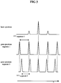
- Figure 3 is a qualitative illustration of the selection of the laser wavelength.
- Two gratings in different segments of the laser have a different spacing of their gain peaks, so their overlap only at one spectral position.
- the resulting laser spectrum is displayed at the top of figure 3 .
- Tuning can be achieved by displacing the two mode combs of the segments relative to each other by a change of the injection currents.
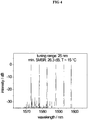
- Figure 4 shows a superposition of spectra recorded from a tuneable DFB. Each spectrum was measured for a specific setting of the injection currents in the segments. The spacing of the emission lines corresponds to the spacing of the gain peaks in the segments.
- Figure 5 shows the additional possibility of tuning the DFB laser to an emission wavelength between the discrete spectral positions determined by the gratings.
- fine tuning is achieved by a simultaneous variation of the injections currents in all segments and/or a change of the temperature of the laser diode.
Landscapes
- Physics & Mathematics (AREA)
- Condensed Matter Physics & Semiconductors (AREA)
- General Physics & Mathematics (AREA)
- Electromagnetism (AREA)
- Optics & Photonics (AREA)
- Semiconductor Lasers (AREA)
Claims (10)
- Mehrsegment-Halbleiter-Laser, umfassend:ein Halbleitersubstrat (11);eine Laserschicht (13), die auf dem Halbleitersubstrat (11) angeordnet ist;ein Wellenleitersteg (15), der in mehrere Segmente geteilt ist und mit Abstand zur Laserschicht (13) angeordnet ist,eine streifenförmige Gitterstruktur (23), die seitlich zu zumindest zwei der Segmente angeordnet ist, wobei die Gitterstruktur (23) zwei strukturelle Bereiche umfasst, die an beiden Seiten des Wellenleiterstegs (15) angeordnet sind und mit Abstand zur Laserschicht (13) über der Laserschicht (13) gebildet sind, undwobei die Gitterstruktur (23) aus zumindest zwei der Segmente aus mehreren Gittern mit verschiedenen Gitterperioden innerhalb des Segments zusammengesetzt sind, mehrere Absorptionsminima bei unterschiedlichen Wellenlängen bereitstellend.
- Mehrsegment-Halbleiter-Laser nach Anspruch 1, wobei der aktive Bereich der Laserschicht (13) aus einer Schicht von Quantenpunkten oder mehreren Quantentöpfen mit unterschiedlicher Zusammensetzung oder Dicke besteht.
- Mehrsegment-Halbleiter-Laser nach Anspruch 1, wobei die Gitterstruktur (23) auf einer Sperr- oder Isolierschicht angeordnet ist, die eine Position der Gitterstruktur (23) relativ zur Laserschicht definiert.
- Mehrsegment-Halbleiter-Laser nach Anspruch 1, wobei die Gitterstruktur (23) aus Metall erzeugt ist.
- Mehrsegment-Halbleiter-Laser nach Anspruch 4, wobei das Metall Chrom oder eine Chromlegierung ist.
- Mehrsegment-Halbleiter-Laser nach Anspruch 1, wobei strukturelle Bereiche der Gitterstruktur (23) angrenzend an Seiten des Wellenleiterstegs angeordnet sind und die Breite des Wellenleiterstegs (15) so dimensioniert ist, dass die Basispunkte von Seiten des Wellenleiterstegs (15) in einem peripheren Strahlungsbereich von einer aktiven Zone der Laserschicht (13) gelegen sind.
- Verfahren zur Herstellung eines Mehrsegment-Halbleiter-Lasers, basierend auf einem Halbleitersubstrat (11) mit einer Laserschicht (12), die auf dem Halbleitersubstrat angeordnet ist, und einer streifenförmigen Gitterstruktur (23), wobei der Verfahren die Schritte umfasst:Erzeugen einer vollständigen Halbleiter-Laser-Struktur in einem epitaktischen Verfahren;Bilden eines Wellenleiterstegs (15), der durch Unterziehen der Halbleiter-Laser-Struktur einem Materialentfernungsverfahren, um Trägerflächen (24, 25) an beiden Seiten eines Wellenleiterstegs (15) zu bilden, in einige Segmente geteilt ist; undAnbringen der Gitterstruktur (23), die aus einer Zusammensetzung mehrerer Gitter mit verschiedenen Gitterperioden innerhalb eines einzelnen Segments besteht, mehrere Absorptionsminima bei verschiedenen Wellenlängen bereitstellend, an den Trägerflächen (24, 25).
- Verfahren nach Anspruch 7, wobei vor dem Anwenden der Gitterstruktur (23) an die Trägerflächen eine Isolierschicht (26) auf den Trägerflächen (24, 25) gebildet ist.
- Verfahren nach Anspruch 8, wobei der Schritt zum Anbringen der Gitterstruktur (23) ein Anbringen einer metallischen Gitterstruktur (23) mit einem Lithografieverfahren enthält, wobei das Lithografieverfahren gefolgt von einer Metallisierung der Lithografiestruktur angewendet wird.
- Verfahren nach Anspruch 9, wobei mehrere Mehrsegment-Halbleiter-Laser in einem Kompositwafer gemäß den Schritten erzeugt werden, umfassend:Erzeugen eines Halbleiter-Laser-Wafers durch Anbringen einer epitaktischen Struktur an einem Halbleitersubstrat;Bilden der stegartigen Wellenleiterstruktur, die Wellenleiterstege umfasst, die aus mehreren Segmenten bestehen und sich parallel zueinander auf der Fläche des Halbleiter-Laser-Wafers erstrecken;Teilen des Halbleiter-Laser-Wafers in einzelne Halbleiter-Laser-Chipeinheiten;Bilden einer oder mehrerer Gitterstrukturen auf den Halbleiter-Laser-Chipeinheiten.
Priority Applications (1)
| Application Number | Priority Date | Filing Date | Title |
|---|---|---|---|
| EP01124821.8A EP1304780B1 (de) | 2001-10-18 | 2001-10-18 | Breitverstimmbarer Halbleiterlaser mit Gitterstruktur |
Applications Claiming Priority (1)
| Application Number | Priority Date | Filing Date | Title |
|---|---|---|---|
| EP01124821.8A EP1304780B1 (de) | 2001-10-18 | 2001-10-18 | Breitverstimmbarer Halbleiterlaser mit Gitterstruktur |
Publications (2)
| Publication Number | Publication Date |
|---|---|
| EP1304780A1 EP1304780A1 (de) | 2003-04-23 |
| EP1304780B1 true EP1304780B1 (de) | 2017-05-10 |
Family
ID=8178997
Family Applications (1)
| Application Number | Title | Priority Date | Filing Date |
|---|---|---|---|
| EP01124821.8A Expired - Lifetime EP1304780B1 (de) | 2001-10-18 | 2001-10-18 | Breitverstimmbarer Halbleiterlaser mit Gitterstruktur |
Country Status (1)
| Country | Link |
|---|---|
| EP (1) | EP1304780B1 (de) |
Families Citing this family (2)
| Publication number | Priority date | Publication date | Assignee | Title |
|---|---|---|---|---|
| DE102007013173A1 (de) | 2007-03-20 | 2008-09-25 | Rottenkolber, Matthias, Dr. | Durchstimmbarer Halbleiterlaser |
| DE102007013470A1 (de) | 2007-03-21 | 2008-09-25 | Rottenkolber, Matthias, Dr. | Direkt durchstimmbarer Halbleiterlaser mit Piezotranslator |
Citations (2)
| Publication number | Priority date | Publication date | Assignee | Title |
|---|---|---|---|---|
| EP0267667A2 (de) * | 1986-11-08 | 1988-05-18 | Stc Plc | Laser mit verteilter Rückkopplung |
| US6208793B1 (en) * | 1997-03-01 | 2001-03-27 | Deutsche Telekom Ag | Wavelength-tunable optoelectronic apparatus |
Family Cites Families (1)
| Publication number | Priority date | Publication date | Assignee | Title |
|---|---|---|---|---|
| US6104739A (en) * | 1997-12-24 | 2000-08-15 | Nortel Networks Corporation | Series of strongly complex coupled DFB lasers |
-
2001
- 2001-10-18 EP EP01124821.8A patent/EP1304780B1/de not_active Expired - Lifetime
Patent Citations (2)
| Publication number | Priority date | Publication date | Assignee | Title |
|---|---|---|---|---|
| EP0267667A2 (de) * | 1986-11-08 | 1988-05-18 | Stc Plc | Laser mit verteilter Rückkopplung |
| US6208793B1 (en) * | 1997-03-01 | 2001-03-27 | Deutsche Telekom Ag | Wavelength-tunable optoelectronic apparatus |
Non-Patent Citations (3)
| Title |
|---|
| DATABASE INSPEC [online] THE INSTITUTION OF ELECTRICAL ENGINEERS, STEVENAGE, GB; 1998, PING ZHOU ET AL: "A binary correlation matrix memory k-NN classifier with hardware implementation", Database accession no. 6208793 * |
| PROCEEDINGS OF BRITISH MACHINE VISION CONFERENCE 14-17 SEPT. 1998 SOUTHAMPTON, UK, vol. 1, BMVC 98. PROCEEDINGS OF THE NINTH BRITISH MACHINE VISION CONFERENCE UNIV. SOUTHAMPTON SOUTHAMPTON, UK, pages 214 - 223 VOL.1, ISBN: 1-901725-04-9 * |
| TOHMORI Y ED - INSTITUTE OF ELECTRICAL AND ELECTRONICS ENGINEERS: "Broadly tunable lasers with a super structure grating", PROCEEDINGS OF THE INTERNATIONAL CONFERENCE ON INDIUM PHOSPHIDE AND RELATED MATERIALS. SANTA BARBARA, MAR. 27 - 31, 1994; [PROCEEDINGS OF THE INTERNATIONAL CONFERENCE ON INDIUM PHOSPHIDE AND RELATED MATERIALS], NEW YORK, IEEE, US, vol. CONF. 6, 27 March 1994 (1994-03-27), pages 29 - 32, XP010118948, ISBN: 978-0-7803-1476-4, DOI: 10.1109/ICIPRM.1994.328152 * |
Also Published As
| Publication number | Publication date |
|---|---|
| EP1304780A1 (de) | 2003-04-23 |
Similar Documents
| Publication | Publication Date | Title |
|---|---|---|
| US7696098B2 (en) | Tuneable unipolar lasers | |
| EP1343232B1 (de) | Ein Halbleiterlaserarray mit seitlicher Gratingstruktur | |
| CN111916997B (zh) | 基于空气孔的分布式反馈激光器及制备方法 | |
| US6594298B2 (en) | Multi-wavelength semiconductor laser array and method for fabricating the same | |
| JP2008113041A (ja) | 導波管 | |
| US5394429A (en) | Distributed-feedback laser with improved analog modulation distortion characteristics and method for fabricating the same | |
| CN107565381B (zh) | 分布反馈式半导体激光器装置及光子集成发射芯片模块 | |
| US7981707B2 (en) | Method for enhancing optical characteristics of multilayer optoelectronic components | |
| CN112670823B (zh) | 电吸收调制激光器的制作方法 | |
| US6671306B1 (en) | Semiconductor laser with a lattice structure | |
| US6846689B2 (en) | Semiconductor laser with a lattice structure | |
| EP1304780B1 (de) | Breitverstimmbarer Halbleiterlaser mit Gitterstruktur | |
| CN120749532A (zh) | 一种新型电吸收调制激光器的制备方法及结构 | |
| TW406441B (en) | Semiconductor laser and method for manufacturing the same | |
| CN106099639A (zh) | 一种多波长阵列激光器及其制造方法和使用方法 | |
| JPH0961652A (ja) | 半導体光導波路およびその作製方法 | |
| CN113224638A (zh) | 一种利用电极来实现取样的sbg半导体激光器装置 | |
| US20060120428A1 (en) | Distributed feedback (DFB) semiconductor laser and fabrication method thereof | |
| KR20030069879A (ko) | 반도체레이저 및 이를 포함하는 광집적반도체소자의제조방법 | |
| CN115085010B (zh) | 可调谐面发射激光器阵列及制作方法 | |
| JPH0724324B2 (ja) | 半導体レーザ・チップおよびその製造方法 | |
| KR100587712B1 (ko) | 자기정렬 릿지 도파로의 반도체 레이저 다이오드 구조 | |
| JP2924041B2 (ja) | モノリシック集積型半導体光素子 | |
| KR100368323B1 (ko) | 이득 결합형 단일모드 반도체 레이저의 제조 방법 | |
| US20080279243A1 (en) | Distributed Feedback (Dfb) Quantum Dot Laser Structure |
Legal Events
| Date | Code | Title | Description |
|---|---|---|---|
| PUAI | Public reference made under article 153(3) epc to a published international application that has entered the european phase |
Free format text: ORIGINAL CODE: 0009012 |
|
| AK | Designated contracting states |
Designated state(s): AT BE CH CY DE DK ES FI FR GB GR IE IT LI LU MC NL PT SE TR |
|
| AX | Request for extension of the european patent |
Extension state: AL LT LV MK RO SI |
|
| 17P | Request for examination filed |
Effective date: 20031015 |
|
| AKX | Designation fees paid |
Designated state(s): AT BE CH CY DE DK ES FI FR GB GR IE IT LI LU MC NL PT SE TR |
|
| 17Q | First examination report despatched |
Effective date: 20061023 |
|
| RAP1 | Party data changed (applicant data changed or rights of an application transferred) |
Owner name: NANOPLUS NANOSYSTEMS AND TECHNOLOGIES GMBH |
|
| GRAP | Despatch of communication of intention to grant a patent |
Free format text: ORIGINAL CODE: EPIDOSNIGR1 |
|
| INTG | Intention to grant announced |
Effective date: 20161207 |
|
| GRAJ | Information related to disapproval of communication of intention to grant by the applicant or resumption of examination proceedings by the epo deleted |
Free format text: ORIGINAL CODE: EPIDOSDIGR1 |
|
| GRAS | Grant fee paid |
Free format text: ORIGINAL CODE: EPIDOSNIGR3 |
|
| GRAP | Despatch of communication of intention to grant a patent |
Free format text: ORIGINAL CODE: EPIDOSNIGR1 |
|
| INTC | Intention to grant announced (deleted) | ||
| RIN1 | Information on inventor provided before grant (corrected) |
Inventor name: KAMP, MARTIN Inventor name: MUELLER, MARTIN |
|
| INTG | Intention to grant announced |
Effective date: 20170221 |
|
| GRAA | (expected) grant |
Free format text: ORIGINAL CODE: 0009210 |
|
| AK | Designated contracting states |
Kind code of ref document: B1 Designated state(s): AT BE CH CY DE DK ES FI FR GB GR IE IT LI LU MC NL PT SE TR |
|
| REG | Reference to a national code |
Ref country code: GB Ref legal event code: FG4D |
|
| REG | Reference to a national code |
Ref country code: AT Ref legal event code: REF Ref document number: 893239 Country of ref document: AT Kind code of ref document: T Effective date: 20170515 Ref country code: CH Ref legal event code: EP |
|
| REG | Reference to a national code |
Ref country code: IE Ref legal event code: FG4D |
|
| REG | Reference to a national code |
Ref country code: DE Ref legal event code: R096 Ref document number: 60150437 Country of ref document: DE |
|
| REG | Reference to a national code |
Ref country code: NL Ref legal event code: MP Effective date: 20170510 |
|
| REG | Reference to a national code |
Ref country code: AT Ref legal event code: MK05 Ref document number: 893239 Country of ref document: AT Kind code of ref document: T Effective date: 20170510 |
|
| PG25 | Lapsed in a contracting state [announced via postgrant information from national office to epo] |
Ref country code: AT Free format text: LAPSE BECAUSE OF FAILURE TO SUBMIT A TRANSLATION OF THE DESCRIPTION OR TO PAY THE FEE WITHIN THE PRESCRIBED TIME-LIMIT Effective date: 20170510 Ref country code: GR Free format text: LAPSE BECAUSE OF FAILURE TO SUBMIT A TRANSLATION OF THE DESCRIPTION OR TO PAY THE FEE WITHIN THE PRESCRIBED TIME-LIMIT Effective date: 20170811 Ref country code: FI Free format text: LAPSE BECAUSE OF FAILURE TO SUBMIT A TRANSLATION OF THE DESCRIPTION OR TO PAY THE FEE WITHIN THE PRESCRIBED TIME-LIMIT Effective date: 20170510 Ref country code: ES Free format text: LAPSE BECAUSE OF FAILURE TO SUBMIT A TRANSLATION OF THE DESCRIPTION OR TO PAY THE FEE WITHIN THE PRESCRIBED TIME-LIMIT Effective date: 20170510 |
|
| PG25 | Lapsed in a contracting state [announced via postgrant information from national office to epo] |
Ref country code: NL Free format text: LAPSE BECAUSE OF FAILURE TO SUBMIT A TRANSLATION OF THE DESCRIPTION OR TO PAY THE FEE WITHIN THE PRESCRIBED TIME-LIMIT Effective date: 20170510 Ref country code: SE Free format text: LAPSE BECAUSE OF FAILURE TO SUBMIT A TRANSLATION OF THE DESCRIPTION OR TO PAY THE FEE WITHIN THE PRESCRIBED TIME-LIMIT Effective date: 20170510 |
|
| PG25 | Lapsed in a contracting state [announced via postgrant information from national office to epo] |
Ref country code: DK Free format text: LAPSE BECAUSE OF FAILURE TO SUBMIT A TRANSLATION OF THE DESCRIPTION OR TO PAY THE FEE WITHIN THE PRESCRIBED TIME-LIMIT Effective date: 20170510 |
|
| REG | Reference to a national code |
Ref country code: DE Ref legal event code: R097 Ref document number: 60150437 Country of ref document: DE |
|
| PG25 | Lapsed in a contracting state [announced via postgrant information from national office to epo] |
Ref country code: IT Free format text: LAPSE BECAUSE OF FAILURE TO SUBMIT A TRANSLATION OF THE DESCRIPTION OR TO PAY THE FEE WITHIN THE PRESCRIBED TIME-LIMIT Effective date: 20170510 |
|
| PLBE | No opposition filed within time limit |
Free format text: ORIGINAL CODE: 0009261 |
|
| STAA | Information on the status of an ep patent application or granted ep patent |
Free format text: STATUS: NO OPPOSITION FILED WITHIN TIME LIMIT |
|
| 26N | No opposition filed |
Effective date: 20180213 |
|
| PG25 | Lapsed in a contracting state [announced via postgrant information from national office to epo] |
Ref country code: MC Free format text: LAPSE BECAUSE OF FAILURE TO SUBMIT A TRANSLATION OF THE DESCRIPTION OR TO PAY THE FEE WITHIN THE PRESCRIBED TIME-LIMIT Effective date: 20170510 |
|
| REG | Reference to a national code |
Ref country code: CH Ref legal event code: PL |
|
| GBPC | Gb: european patent ceased through non-payment of renewal fee |
Effective date: 20171018 |
|
| REG | Reference to a national code |
Ref country code: IE Ref legal event code: MM4A |
|
| REG | Reference to a national code |
Ref country code: FR Ref legal event code: ST Effective date: 20180629 |
|
| PG25 | Lapsed in a contracting state [announced via postgrant information from national office to epo] |
Ref country code: GB Free format text: LAPSE BECAUSE OF NON-PAYMENT OF DUE FEES Effective date: 20171018 Ref country code: LI Free format text: LAPSE BECAUSE OF NON-PAYMENT OF DUE FEES Effective date: 20171031 Ref country code: LU Free format text: LAPSE BECAUSE OF NON-PAYMENT OF DUE FEES Effective date: 20171018 Ref country code: CH Free format text: LAPSE BECAUSE OF NON-PAYMENT OF DUE FEES Effective date: 20171031 |
|
| REG | Reference to a national code |
Ref country code: BE Ref legal event code: MM Effective date: 20171031 |
|
| PG25 | Lapsed in a contracting state [announced via postgrant information from national office to epo] |
Ref country code: FR Free format text: LAPSE BECAUSE OF NON-PAYMENT OF DUE FEES Effective date: 20171031 Ref country code: BE Free format text: LAPSE BECAUSE OF NON-PAYMENT OF DUE FEES Effective date: 20171031 |
|
| PG25 | Lapsed in a contracting state [announced via postgrant information from national office to epo] |
Ref country code: IE Free format text: LAPSE BECAUSE OF NON-PAYMENT OF DUE FEES Effective date: 20171018 |
|
| PG25 | Lapsed in a contracting state [announced via postgrant information from national office to epo] |
Ref country code: CY Free format text: LAPSE BECAUSE OF NON-PAYMENT OF DUE FEES Effective date: 20170510 |
|
| PG25 | Lapsed in a contracting state [announced via postgrant information from national office to epo] |
Ref country code: TR Free format text: LAPSE BECAUSE OF FAILURE TO SUBMIT A TRANSLATION OF THE DESCRIPTION OR TO PAY THE FEE WITHIN THE PRESCRIBED TIME-LIMIT Effective date: 20170510 |
|
| PG25 | Lapsed in a contracting state [announced via postgrant information from national office to epo] |
Ref country code: PT Free format text: LAPSE BECAUSE OF FAILURE TO SUBMIT A TRANSLATION OF THE DESCRIPTION OR TO PAY THE FEE WITHIN THE PRESCRIBED TIME-LIMIT Effective date: 20170510 |
|
| PGFP | Annual fee paid to national office [announced via postgrant information from national office to epo] |
Ref country code: DE Payment date: 20210318 Year of fee payment: 20 |
|
| REG | Reference to a national code |
Ref country code: DE Ref legal event code: R071 Ref document number: 60150437 Country of ref document: DE |