EP1304807A1 - Procédé et dispositif de conversion analogique/numérique fléxible - Google Patents
Procédé et dispositif de conversion analogique/numérique fléxible Download PDFInfo
- Publication number
- EP1304807A1 EP1304807A1 EP02023418A EP02023418A EP1304807A1 EP 1304807 A1 EP1304807 A1 EP 1304807A1 EP 02023418 A EP02023418 A EP 02023418A EP 02023418 A EP02023418 A EP 02023418A EP 1304807 A1 EP1304807 A1 EP 1304807A1
- Authority
- EP
- European Patent Office
- Prior art keywords
- analog
- adc
- configuration parameter
- digital conversion
- control logic
- Prior art date
- Legal status (The legal status is an assumption and is not a legal conclusion. Google has not performed a legal analysis and makes no representation as to the accuracy of the status listed.)
- Withdrawn
Links
- 238000006243 chemical reaction Methods 0.000 title claims abstract description 140
- 238000000034 method Methods 0.000 title claims description 45
- 230000007246 mechanism Effects 0.000 claims abstract description 59
- 230000001351 cycling effect Effects 0.000 claims description 6
- 238000012544 monitoring process Methods 0.000 abstract description 10
- 230000008859 change Effects 0.000 abstract description 7
- 230000008569 process Effects 0.000 description 24
- 238000005259 measurement Methods 0.000 description 22
- 238000010586 diagram Methods 0.000 description 8
- 238000004891 communication Methods 0.000 description 6
- 230000004048 modification Effects 0.000 description 6
- 238000012986 modification Methods 0.000 description 6
- 102100034004 Gamma-adducin Human genes 0.000 description 5
- 101000799011 Homo sapiens Gamma-adducin Proteins 0.000 description 5
- 238000013459 approach Methods 0.000 description 3
- 230000008901 benefit Effects 0.000 description 3
- 238000005516 engineering process Methods 0.000 description 3
- 230000006870 function Effects 0.000 description 3
- 230000003287 optical effect Effects 0.000 description 3
- 238000005070 sampling Methods 0.000 description 3
- HBBGRARXTFLTSG-UHFFFAOYSA-N Lithium ion Chemical compound [Li+] HBBGRARXTFLTSG-UHFFFAOYSA-N 0.000 description 2
- 230000005540 biological transmission Effects 0.000 description 2
- 238000009529 body temperature measurement Methods 0.000 description 2
- 230000000694 effects Effects 0.000 description 2
- 239000000446 fuel Substances 0.000 description 2
- 229910001416 lithium ion Inorganic materials 0.000 description 2
- 230000004075 alteration Effects 0.000 description 1
- 238000004590 computer program Methods 0.000 description 1
- 230000007613 environmental effect Effects 0.000 description 1
- 238000009434 installation Methods 0.000 description 1
- 230000008520 organization Effects 0.000 description 1
- 230000004044 response Effects 0.000 description 1
- 239000004065 semiconductor Substances 0.000 description 1
- 238000012546 transfer Methods 0.000 description 1
Images



Classifications
-
- H—ELECTRICITY
- H03—ELECTRONIC CIRCUITRY
- H03M—CODING; DECODING; CODE CONVERSION IN GENERAL
- H03M1/00—Analogue/digital conversion; Digital/analogue conversion
- H03M1/004—Reconfigurable analogue/digital or digital/analogue converters
-
- H—ELECTRICITY
- H03—ELECTRONIC CIRCUITRY
- H03M—CODING; DECODING; CODE CONVERSION IN GENERAL
- H03M1/00—Analogue/digital conversion; Digital/analogue conversion
- H03M1/004—Reconfigurable analogue/digital or digital/analogue converters
- H03M1/007—Reconfigurable analogue/digital or digital/analogue converters among different resolutions
-
- H—ELECTRICITY
- H03—ELECTRONIC CIRCUITRY
- H03M—CODING; DECODING; CODE CONVERSION IN GENERAL
- H03M1/00—Analogue/digital conversion; Digital/analogue conversion
- H03M1/12—Analogue/digital converters
Definitions
- the invention relates to analog-to-digital conversion and, more particularly, to flexible control of analog-to-digital converters.
- analog-to-digital converters may be configured to convert analog input signals to digital representations of the analog input signals in a substantially continuous fashion; without adjusting the ADC configuration.
- an ADC may operate at top speed on a continuous analog input stream from a single signal.
- the ADC converts a sample of the input stream.
- the ADC may provide an indication that the conversion is complete.
- the digital information may be read out of the ADC by an interface circuit that may include a microprocessor, for example. Subsequent conversions may be initiated by the microprocessor without any modification of the ADC's configuration.
- an analog-to-digital converter (ADC) system may be employed in an application where a number of analog signals must be converted to digital signals.
- the various signals may be multiplexed into the ADC for conversion sequentially.
- Each change in the multiplexor that is, each change in the selection of analog signals for conversion, is a change in the ADC configuration.
- other configuration changes may be used in a given ADC application. For example, one signal may require greater resolution than another, another require a different reference voltage.
- Such configuration changes are typically incorporated in the firmware used to direct the operation of a microprocessor that controls and ADC.
- An ADC that provides configuration flexibility, permitting the use of various resolutions, input channels, voltage references, and conversion sequences, for example, would be highly desirable.
- An analog-to-digital converter in accordance with the principles of the present invention includes read/write storage for at least one configuration parameter value.
- the one or more configuration parameter read/write storage locations are configured to accept configuration information that may be used by control logic to configure the ADC's conversion mechanism. Different configuration information may be downloaded to the read/write storage locations to configure the ADC in a manner that is suited to different applications or circumstances.
- the read/write storage locations may be organized as lists through which the ADC may cycle to reconfigure itself for the conversion of various signals of interest.
- an ADC in accordance with the principles of the present invention includes, a conversion mechanism, an input/output (I/O) interface, control logic, read/write storage, at least one analog input channel, and at least one voltage reference input.
- the conversion mechanism may be any sort of ADC conversion mechanism known in the art, such as a "flash", sigma-delta, integrating, charge-balancing, or successive approximation, for example.
- the control logic may take the form of combinatorial/sequential logic, a state machine, or a microprocessor such as the core microprocessor of an application specific integrated circuit, for example.
- the read/write storage may be implemented as non-volatile memory, such as electrically erasable programmable read only memory (EEPROM), flash memory, or battery-backed random access memory, for example.
- EEPROM electrically erasable programmable read only memory
- flash memory or battery-backed random access memory
- the read/write storage may be used to store configuration parameter values employed by the control logic to control the conversion mechanism.
- the parameter values may be organized within the storage as one or more lists, with each list containing configuration parameter values directed to a particular set of conditions.
- Various list combinations may be employed for different applications. In this way, a standard ADC may be readily "customized" to operate in different applications simply by downloading corresponding sets of parameter lists.
- the control logic may select among the lists in order to accommodate changing conditions. For example, different lists may be associated with operation within different ranges of environmental parameter values and, given the values, the control logic might switch among the lists to operate the ADC with the appropriate set of configuration parameters.
- the new ADC is particularly well suited for operation in battery monitoring and charging applications.
- an ADC may convert a number of cell voltages, operating current, temperature, and other parameters using a variety of reference voltages.
- the converted data may be used to determine remaining battery capacity, for example.
- the battery monitor itself may alter its operation.
- the battery-monitor may measure current (via the ADC) more frequently as the battery is discharged near the end of its useful capacity.
- control logic may load parameters to the ADC from a list that dictates more frequent current measurement.
- analog signals are converted to digital signals at different resolutions and frequencies of conversion, depending on a parameter that may be measured or computed.
- a battery monitor employs an ADC to measure the temperature, voltage and current drain of a battery. Based upon these measurements, the battery monitor determines the battery's state-of-charge. In turn, the state-of-charge determines the frequency, sequence, and resolution of the various analog-to-digital conversions.
- the controller employs various configuration lists that determine the frequency and resolution of the parameter measurements. Additionally, the lists may include a selection among various reference voltages. Greater resolution and frequency of measurement may be employed, for example, in the measurement of battery voltage as the remaining battery capacity reaches a critical point, such as fully charged or fully discharged.
- Loading a value from a configuration list into the ADC may effect a change in conversion resolution.
- the frequency of conversion may be implemented within the list or by varying the lists. That is, within each list each parameter to be measured may be converted a different number of times and "read out" at different speeds. So that, for example, the battery voltage may be converted twenty times in a row at the highest conversion speed provided by the ADC, followed by a single temperature conversion, followed by a twenty more voltage readings, followed by a single current reading. By varying the number of times the readings are made within each "configuration list", the frequency of the readings may be varied within the list. The conversion frequency of all parameters may be varied in this manner.
- the conversion frequency of the various parameters may be varied by shuffling through a variety of lists, each of which may include different sequences of conversion.
- Various combinations of "within-list" conversion frequencies, external-to-list conversion frequencies and modifications of ADC readout speed may be employed to alter the frequency of conversion.
- the battery monitor may also employ such configuration lists to select among a variety of available voltage references for different analog-to-digital conversions.
- An embodiment of the present invention is an analog to digital converter (ADC) comprising:
- the storage can be a read/write storage.
- the plurality of configuration parameters can be stored as one or more lists and the control logic is configured to cycle through at least one list, thereby altering the configuration of the analog-to-digital conversion mechanism.
- the stored configuration parameter value may controls the selection of an analog input channel from which an analog signal is to be converted to a digital signal.
- the stored configuration parameter value may control the resolution of an analog-to-digital conversion.
- the stored configuration parameter value may also control the selection of a reference voltage input from which a reference voltage is obtained for use in an analog-to-digital conversion by the analog-to-digital conversion mechanism.
- the input port can be adapted for receiving said one or more configuration parameter values for storage in said storage.
- a method of converting analog signals to digital signals may comprise the steps of:
- the step of the storing (A) can includes the step of: (A1) storing said one or more configuration parameter values by downloading them to read/write storage included in the ADC that includes the analog-to-digital conversion mechanism. Furthermore, the step of (A2) organizing the stored configuration parameter values as one or more lists can be included.
- the step of configuring (B) may include the step of : (B1) the control logic cycling through at least one list, thereby altering the configuration of the analog-to-digital conversion mechanism. Furthermore, it may include the step of : (B2) the control logic configuring the analog-to-digital conversion mechanism to select an input channel from which an associated analog signal is to be converted to a digital signal.
- the step of configuring (B1) may further include the step of: (B3) the control logic selecting the conversion resolution of the analog-to-digital conversion mechanism and/or the step of: (B4) the control logic selecting a reference voltage input from which a reference voltage is obtained for use in an analog-to-digital conversion by the analog-to-digital conversion mechanism.
- the method may further comprise the step of: the ADC receiving said one or more configuration parameter values through an input port.
- the one or more sensors can include a voltage sensor adapted to sense the voltage across one or more cells of a battery being monitored.
- the one or more sensors can also include a temperature sensor adapted to sense the temperature of a battery being monitored.
- the one or more sensors may also include a current sensor adapted to sense the discharge current of a battery being monitored.
- the configuration parameter values can be arranged in a plurality of configuration lists and the control logic can be adapted to configure the analog-to-digital conversion mechanism from different lists, depending upon the value of one or more of the sensed battery characteristics.
- the configuration parameter values can also be arranged in a plurality of configuration lists and the control logic can be adapted to configure the analog-to-digital conversion mechanism from different lists, depending upon the state of charge of the monitored battery.
- a method of monitoring a battery may comprise the steps of:
- the step of storing may include the step of: (A1) storing said one or more configuration parameter values by downloading them to read/write storage included in the ADC that includes the analog-to-digital conversion mechanism; and/or the step of: (A2) organizing the stored configuration parameter values as one or more lists.
- the step of configuring may include the step of: (B1) the control logic cycling through at least one list, thereby altering the configuration of the analog-to-digital conversion mechanism; and/or the step of: (B2) the control logic configuring the analog-to-digital conversion mechanism to select an input channel from which an associated analog signal is to be converted to a digital signal.
- the step of configuring (B1) may further include the step of: (B3) the control logic selecting the conversion resolution of the analog-to-digital conversion mechanism; and/or the step of: (B4) the control logic selecting a reference voltage input from which a reference voltage is obtained for use in an analog-to-digital conversion by the analog-to-digital conversion mechanism.
- the method may further comprise the step of: the ADC receiving said one or more configuration parameter values through an input port.
- the one or more sensors can include a voltage sensor adapted to sense the voltage across one or more cells of a battery being monitored.
- the one or more sensors can further include a temperature sensor adapted to sense the temperature of a battery being monitored.
- the one or more sensors can also include a current sensor adapted to sense the discharge current of a battery being monitored.
- the configuration parameter values can be arranged in a plurality of configuration lists and the control logic can be adapted to configure the analog-to-digital conversion mechanism from different lists, depending upon the value of one or more of the sensed battery characteristics.
- the configuration parameter values can also be arranged in a plurality of configuration lists and the control logic can be adapted to configure the analog-to-digital conversion mechanism from different lists, depending upon the state of charge of the monitored battery.
- a method of operating an electronics system may comprise the steps of:
- the step of storing (D) can include the step of: (D1) storing said one or more configuration parameter values by downloading them to read/write storage included in the ADC that includes the analog-to-digital conversion mechanism; and/or the step of: (D2) organizing the stored configuration parameter values as one or more lists.
- the step of configuring (F) can include the step of: (F1) the control logic cycling through at least one list, thereby altering the configuration of the analog-to-digital conversion mechanism.
- the step of configuring (F1) can include the step of: (F2) the control logic configuring the analog-to-digital conversion mechanism to select an input channel from which an associated analog signal is to be converted to a digital signal; and or the step of: (F3) the control logic selecting the conversion resolution of the analog-to-digital conversion mechanism.
- the step of configuring (R) can include the step of: (F4) the control logic selecting a reference voltage input from which a reference voltage is obtained for use in an analog-to-digital conversion by the analog-to-digital conversion mechanism.
- the method may further comprise the step of: (H) the ADC receiving said one or more configuration parameter values through an input port.
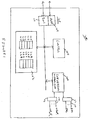
- the ADC 100 includes read/write storage 102 for at least one configuration parameter value.
- the storage 102 may be in the form of non-volatile memory, such as flash, battery-backed, or EEPROM memory, for example.
- ten storage locations are organized as two lists of five locations each, having respective addresses of L1A-L1E and L2A-L2E. Each storage location may be any number of bits wide. For convenience, the storage locations may be organized in byte-wide, or byte-wide multiples.
- the configuration parameter read/write storage locations L1A-L1E and L2A-L2E are configured to accept configuration information that may be used by control logic 104 to configure the ADC's conversion mechanism 106.
- the conversion mechanism 106 may be any sort of ADC conversion mechanism known in the art, such as a "flash”, sigma-delta, integrating, charge-balancing, or successive approximation, for example.
- the control logic 104 may take the form of combinatorial/sequential logic, a state machine, or a microprocessor such as the core microprocessor of an application specific integrated circuit, for example.
- An input/output (I/O) interface 108 may be employed to interact with other, system-level, components, for example, and may include a communications port 109 through which configuration parameter values may be downloaded for storage in the storage locations L1A-L1E and L2A-L2E.
- the port 109 may also include a parallel digital output 111, which may be used to transfer results from the ADC 100.
- One or more input channels 110 may route analog signals 1N1-1Nn to the conversion mechanism 106 for conversion to digital signals.
- a multiplexor 112 may be included in the signal path to select among the analog input channels for conversion.
- One or more voltage reference inputs 114 may also be connected through a path that includes a multiplexor 116 that may be employed to select among a plurality of voltage references Vrefl - Vrefn.
- One or more voltage references, Vrefl - Vrefn may be integral to the ADC 100 or may be separately packaged and accessed through the voltage reference inputs 114.
- Each list of parameter values, located in storage locations L1A-L1E and L2A-L2E, may contain configuration parameter values directed to a different set of conditions.
- One or more ADCs may be "customized" by downloading one or more lists, such as lists L1A-L1E and L2A-L2E, directed toward a specific application. Different list combinations may be employed for different applications.
- the term, "Different list combinations,” includes lists having the same organization and storage locations, but loaded with different parameter values. It also includes lists having different locations and/or organizations.
- the control logic 104 may select among the lists L1A-L1E and L2A-L2E in order to accommodate changing conditions.
- list L1A-L1E may contain ADC configuration data associated with ambient temperatures from 0° to 20°
- list L2A-L2E associated with ambient temperatures from 20° to 30°.
- the control logic 104 could switch from one corresponding list to another in order to configure the ADC conversion mechanism appropriately for the circumstances.
- the block diagram of Figure 2 provides a more detailed view of the illustrative configuration lists L1A-L1E and L2A-L2E.
- the illustrated lists are byte-wide, with three parameter definition fields. Each field is dedicated to a separate configuration parameter related to the ADC conversion mechanism 106.
- bits 0-4 determine the ADC input channel 1N1-1Nn (by controlling the multiplexor 112, for example), bits 5 and 6 determine the conversion speed, by setting the hold time of a sample/hold, for example.
- Bit 7 determines which of two available reference voltage inputs is used (by controlling the multiplexor 116, for example).
- the contents of each location, L1A-L1E and L2A-L2E define the configuration parameters for an ADC conversion.
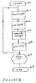
- the flow chart of Figure 3 depicts the operation of an ADC in accordance with the principles of the present invention.
- the process begins in step 300 and proceeds to step 302 where configuration parameter values are stored in the lists, L1 and L2. These values may be downloaded through an input/output interface 108, for example.
- step 302 the process proceeds to step 304, where the control logic 104 retrieves configuration parameter values from one of the lists. Initially, the parameter values are obtained from the "top" location in the list, location L1A in this example. This retrieval process may be initiated, for example, by a power-on-reset routine in an embodiment in which the control logic includes a microprocessor.
- control logic 104 configures the ADC conversion mechanism 106 in conformity with the parameter values retrieved from the storage location L1A.
- the control logic 104 may effect the configuration, for example, by loading a register that controls the multiplexors, 112, 116, and other configurable elements of the ADC.
- Other configurable elements may include conversion speed, sample-and-hold configuration, or conversion resolution, for example. Some of the elements may be inter-related, as in the case of a sigma-delta converter in which resolution and conversion speed are inversely related ( i . e ., greater resolution implies lower conversion speed).
- step 308 the conversion process is initiated.
- the conversion process may include any of various forms of "hand-shaking", so that, for example, once the conversion process has been initiated, the conversion mechanism 106 alerts the control logic, through an interrupt, for example, that a conversion is complete.
- step 310 the control logic 104 determines which is the appropriate location from which to obtain the next set of configuration parameter values.
- the completion of a conversion may be determined through a variety of techniques known in the art, such as an interrupt generated by the conversion mechanism or a control logic timer, for example.
- the results of the conversion may be employed by the control logic, to determine whether conversion parameter values should be obtained from the other list, for example. Additionally, the conversion results may be made available to another functional block or entity and/or stored.
- step 310 If the control logic 104 determines in step 310 that conditions have not changed in a manner that would require alteration of the normal sequence of conversions, the process returns to step 304 and from there, as previously described, to cycle through the configuration changes associated with analog-to-digital conversions.
- the determination of step 310 may include input from elements outside the ADC itself, by means of an interrupt, or message received at the I/O interface, for example.
- the control logic need not return to a configuration parameter list between each ADC conversion; the same configuration data may be employed for more than one conversion.
- step 310 the control logic 104 determines that a different configuration parameter value list should be employed, the control logic goes to the location of the top of the appropriate list (L2A in this example) to obtain the next set of configuration parameters in step 304 and proceeds from there as previously described. As indicated by the "continue" block of step 312 the process proceeds in this manner indefinitely until, due to a shutdown, for example, it proceeds to end in step 314. Other operations, such as the downloading of additional configuration parameter lists or the modification of existing lists may occur, for example, during the "continue" phase of step 312.
- FIG. 4 provides a more detailed view of an ADC 100 in accordance with the principles of the present invention.
- the ADC is employed as a battery monitor and the conversion mechanism 106 is a fourteen bit sigma-delta integrating A/D.
- the I/O port 108 includes a bus interface 400 and a programmable digital input/output 402.
- Storage 102 includes EEPROM 404 and a one time programmable (OTP) EPROM 406.
- the control logic 104 includes a microcontroller core 408.
- the ADC 100 includes a voltage regulator 410 and an oscillator and bias circuitry 412. At least one voltage reference and temperature sensor 414 are included.
- An input multiplexor 416 operates under control of the microcontroller 408 to select an analog signal of interest for conversion.
- the analog input signals include four cell voltages Vcell1 Vcell2, Vcell3, and Vcell4.
- the analog inputs also include shunt resistor inputs VSHN and VSHP, which may be used to sense the current drawn from a battery being monitored, and external thermistor inputs VNTC and VREFT, which may be used to measure the temperature of a battery pack.
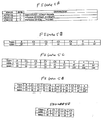
- the table of Figure 5A provides an illustrative bit-field definition for configuration parameter values storage in accordance with the principles of the present invention.
- bits 0-2 Analog Digital Definition - ADD
- bits 0-2 Analog Digital Definition - ADD
- Selections range from a binary value of "0”, which provides 8-bit resolution, to a binary value of "7" ( i.e. , 111), which provides 15-bit resolution.
- Bits 4 through 7 (ADD4 - ADD7) determine which one of sixteen input channels is selected for the analog-to-digital conversion of its associated signal.
- the table of Figure 5B illustrates a list of configuration parameter values in accordance with the principles of the present invention.
- the actual list entries are presented in hexadecimal format (e . g ., the contents of the last list location are "6F", which corresponds to a binary value of "0110 1111").
- the entry types, P, C1, C2, C3, C4, T, and I provide a "shorthand" indication of the function associated with the corresponding contents.
- a "P" entry indicates that the analog signal to be converted represents the voltage across an entire battery "pack", that is, from one pole of a cell at one extreme of the pack to the opposite pole of the cell at the other extreme of the pack.
- Entries C1, C2, C3, and C4 indicate that the analog signals to be converted respectively correspond to the first, second, third, and fourth cells of a multi-cell stack.
- a current measurement is indicated by an "I” entry
- a temperature measurement is indicated by a "T” entry.
- a temperature measurement, indicated by a "T” type entry employs 15-bit resolution, whereas other conversions employ 11-bit resolution.
- the microcontroller 408 would cycle through such a list, reconfiguring the ADC conversion mechanism 106 before each conversion according to the list entry. That is, the first conversion associated with the list of Figure 5B would be a "P"-configured conversion, which would provide a digitized indication of the pack voltage. The following conversion would be a "C1" (cell 1) type of conversion, followed by a "C2" conversion, and so on.
- a basic conversion parameter list, such as that of Figure 5B could be cycled through repeatedly, with the substantially equal time devoted to the conversion of all analog inputs of interest. In a sigma-delta converter embodiment such as this illustrative example, the conversion speed is inversely related to the conversion resolution.
- the frequency of sampling may be varied by changing the list, by adding another P-type entry, for example, or through other list adjustments. Additionally, a plurality of lists, each having a different set of entries, may be cycled through in order to vary the frequency of measurement.
- current measurements are typically made more frequently than in the example of Figure 5B. Because the list of Figure 5C includes three current measurements, such a list may be better suited to a battery fuel gauge application than the list of Figure 5B.
- the third row of Figure 5C includes illustrative conversion times for the various configurations.
- cell voltage is used as the criteria for determining "full” or “empty” status in a Lithium Ion battery pack and cell voltages change more rapidly as the battery approaches either the full or empty state. Consequently, the importance of measuring cell voltages in a Lithium Ion battery pack increases as the battery approaches either the "full” or "empty” state-of-charge.
- a configuration list such as that of Figure 5D, may be employed in such circumstances. Such a list yields cell voltage measurements twice every 520 msec, in contrast to once every 1080 msec using the list of Figure 5C.
- the configuration list of Figure 5E may be employed to calibrate pack and cell voltages, for example. Each voltage of interest is measured once every 100 msec in this example and no time is devoted to the measurement of parameters, such as current or temperature, that are not of interest at the time voltages are being calibrated.
- the flow chart of Figure 6 illustrates the operation of a battery monitor/controller in accordance with the principles of the present invention, particularly in relation to the operation of a list-configured ADC, as previously described.
- the process begins in step 600 then proceeds to step 602 where configuration lists for the ADC are downloaded.
- the downloaded lists may include configuration lists directed to specific operations, to specific battery chemistries, or to the number of cells in a the battery, for example.
- the lists may include calibration lists, which emphasize the measurement of cell or battery-pack voltage, and there may be "normal operation", "battery full” and "battery low” lists, for example.
- the process proceeds to step 604 where the battery monitor/charger is calibrated. Lists downloaded in step 602 may be employed in this calibration process. A system-level calibration, including that of whatever electronic system may be using the battery pack for system power, may be effected in this step too.
- step 606 the monitor/charger undertakes the monitoring and charging of an associated battery.
- the battery, monitor, and charger may all be incorporated in an electronic device, such as a handheld or laptop computer, for example.
- the monitor and charging control process may employ any of a variety of techniques known in the art. For example, charging techniques set forth in U.S. Patent No. , issued to , in , or in U.S. Patent No. , issued to , in , which are hereby incorporated by reference in their entirety, may be employed during the monitoring/charging stage of this process.
- This process may include the use of various ADC configuration lists, as previously described, to alter the ADC configuration parameters and to thereby accommodate charging processes that vary the types of measurement, frequency, resolution, reference voltage, quantity of interest, e.g., depending upon the state-of-charge.
- the state-of-charge factors may include current, temperature, voltage, and charge/discharge history.
- the frequency of measurement (measurement entails A/D conversion in this context) may be controlled within a list, by including such measurements more or less frequently within a given list, or by switching from list to list, with some lists including more frequent measurements of a given parameter than others.
- the ADC operation during this phase is related to gathering information related to a battery's state-of-charge, issuing alarms, as appropriate, and controlling current flow, when charging current is available.
- Different ADC configuration lists may be associated with different phases of this operation.
- the monitoring/charging phase could last indefinitely and proceed to end in step 610 only with the end of the battery or the equipment using it.
- decision block 612 given the right set of circumstances, the process could return to step 602, where another set of ADC configuration lists is downloaded.
- Such a downloading may occur, for example, diagnostics are run on the battery, the battery monitor, or the electronic equipment using the battery.
- the battery monitor could be "swapped out" for use with a different battery pack and that pack may include a different number of cells or different cell chemistry, for example. In that case, the new ADC configuration lists downloaded in step 602 would accommodate the new battery pack.
- FIG. 7 depicts an electronic system 700, which employs a battery monitor/charger in accordance with the principles of the present invention.
- a battery monitor 702 employs one or more configuration lists as previously described in conjunction with an ADC to measure various parameters associated with a battery-pack 704. The measured parameters might include one or more temperatures, discharge current, or cell and/or pack voltages, for example. Additionally, a plurality of voltage references may be employed in the ADC conversion process, with the selection of voltage reference determined by the contents of the configuration lists.
- the battery-pack 704 supplies "primary" or “backup” energy to system electronics 706.
- a battery monitor/charger in accordance with the principles of the present invention may be applied to a wide range of electronic systems 700.
- the system 700 may range in size and battery capacity from a handheld electronic device to transportation device such as a battery- or hybrid-powered car or bus, to an industrial installation. Monitoring information obtained by the monitor is supplied to a charge controller 708 which controls the amount of charging current supplied to the battery-pack 704 from an external source 710 when that source is available.
- the monitor 702 may include communications links 712, 714, 716, and 718 to the charger, battery pack, system electronics and external electronics.
- the link 712 with the charger may be used to convey battery-pack status information and may also permit the charger 708 to query the monitor 702.
- the link 714 with the battery-pack includes various analog signal lines, which permit the monitor to measure cell voltages, and other parameters as previously described.
- the link 716 may permit system electronics 706 to download configuration lists to the monitor 702, for example and the link 718 may permit the downloading of configuration lists from external electronics to the monitor.
- a software implementation of the above described embodiment(s) may comprise a series of computer instructions either fixed on a tangible medium, such as a computer readable media, e.g. diskette, CD-ROM, ROM, or fixed disc, or transmittable to a computer system, via a modem or other interface device, such as communications adapter connected to the network over a medium.
- Medium can be either a tangible medium, including but not limited to, optical or analog communications lines, or may be implemented with wireless techniques, including but not limited to microwave, infrared or other transmission techniques.
- the series of computer instructions embodies all or part of the functionality previously described herein with respect to the invention. Those skilled in the art will appreciate that such computer instructions can be written in a number of programming languages for use with many computer architectures or operating systems.
- Such instructions may be stored using any memory technology, present or future, including, but not limited to, semiconductor, magnetic, optical or other memory devices, or transmitted using any communications technology, present or future, including but not limited to optical, infrared, microwave, or other transmission technologies.
- a computer program product may be distributed as a removable media with accompanying printed or electronic documentation, e.g. , shrink wrapped software, preloaded with a computer system, e.g. , on system ROM or fixed disc, or distributed from a server or electronic bulletin board over a network, e.g., the Internet or World Wide Web.
- the methods of the invention may be achieved in either all software implementations, using the appropriate object or processor instructions, or in hybrid implementations that utilize a combination of hardware logic, software logic and/or firmware to achieve the same results.
- Processes illustrated through the use of flow charts may not be strictly linear processes and alternative flows may be implemented within the scope of the invention.
- the specific configuration of logic and/or inst ructions utilized to achieve a particular function, as well as other modifications to the inventive concept are intended to be covered by the appended claims.
Landscapes
- Engineering & Computer Science (AREA)
- Theoretical Computer Science (AREA)
- Secondary Cells (AREA)
- Analogue/Digital Conversion (AREA)
Applications Claiming Priority (4)
| Application Number | Priority Date | Filing Date | Title |
|---|---|---|---|
| US33513701P | 2001-10-19 | 2001-10-19 | |
| US335137P | 2001-10-19 | ||
| US147250 | 2002-05-16 | ||
| US10/147,250 US20030076250A1 (en) | 2001-10-19 | 2002-05-16 | Method and apparatus for flexible analog-to-digital conversion |
Publications (1)
| Publication Number | Publication Date |
|---|---|
| EP1304807A1 true EP1304807A1 (fr) | 2003-04-23 |
Family
ID=26844744
Family Applications (1)
| Application Number | Title | Priority Date | Filing Date |
|---|---|---|---|
| EP02023418A Withdrawn EP1304807A1 (fr) | 2001-10-19 | 2002-10-19 | Procédé et dispositif de conversion analogique/numérique fléxible |
Country Status (2)
| Country | Link |
|---|---|
| US (1) | US20030076250A1 (fr) |
| EP (1) | EP1304807A1 (fr) |
Cited By (1)
| Publication number | Priority date | Publication date | Assignee | Title |
|---|---|---|---|---|
| WO2020081443A1 (fr) * | 2018-10-16 | 2020-04-23 | Microchip Technology Incorporated | Contrôleurs de convertisseur analogique-numérique comprenant des contextes configurables |
Families Citing this family (10)
| Publication number | Priority date | Publication date | Assignee | Title |
|---|---|---|---|---|
| US7970560B2 (en) * | 2005-10-11 | 2011-06-28 | Phoenix Broadband Technologies, Llc | Method and apparatus for measuring and monitoring a power source |
| DE102006003566B4 (de) * | 2006-01-25 | 2020-10-01 | Infineon Technologies Ag | Signal-Wandel-Vorrichtung, insbesondere Analog-Digital-Wandel-Vorrichtung, und Verfahren zum Betreiben einer Signal-Wandel-Vorrichtung |
| DE102006009033B4 (de) * | 2006-02-27 | 2013-10-24 | Infineon Technologies Ag | Signal-Wandel-Vorrichtung, insbesondere Analog-Digital-Wandel-Vorrichtung, und Verfahren zum Betreiben einer Signal-Wandel-Vorrichtung |
| US11218003B2 (en) * | 2009-09-22 | 2022-01-04 | Phoenix Broadband Technologies, Llc | Method and apparatus for intelligent battery charge equalization and monitoring |
| US10365332B2 (en) | 2012-11-02 | 2019-07-30 | Analog Devices Global Unlimited Company | System and method to reduce data handling on lithium ion battery monitors |
| US9712178B2 (en) * | 2013-05-03 | 2017-07-18 | Texas Instruments Incorporated | Dynamic resolution adjustment for digital converters |
| US10295608B2 (en) | 2014-07-18 | 2019-05-21 | Phoenix Broadband Technologies, Llc | Non-intrusive correlating battery monitoring system and method |
| US10305312B2 (en) * | 2016-11-08 | 2019-05-28 | Lenovo (Singapore) Pte. Ltd. | Supplemental power system for battery powered device |
| JP6869884B2 (ja) * | 2017-12-26 | 2021-05-12 | 株式会社日立製作所 | センサ端末およびセンサシステム |
| JP7573236B2 (ja) * | 2020-09-28 | 2024-10-25 | パナソニックIpマネジメント株式会社 | Ad変換器、及びそれを備えるセンサシステム |
Citations (5)
| Publication number | Priority date | Publication date | Assignee | Title |
|---|---|---|---|---|
| US5363031A (en) * | 1989-12-05 | 1994-11-08 | Norand Corporation | Fast battery charger |
| WO1997012310A2 (fr) * | 1995-09-11 | 1997-04-03 | Microchip Technology Incorporated | Extraction numerique pour composants analogiques de micro-circuits |
| US6047380A (en) * | 1995-09-19 | 2000-04-04 | Microchip Technology Incorporated | Microcontroller wake-up function having an interleaving priority scheme for sampling a plurality of analog input signals |
| WO2001010031A2 (fr) * | 1999-08-02 | 2001-02-08 | Infineon Technologies Ag | Procede de conversion de signaux analogiques en signaux numeriques et dispositif convertisseur analogique/numerique correspondant |
| WO2001063770A1 (fr) * | 2000-02-22 | 2001-08-30 | Burr-Brown Corporation | Convertisseur analogique numerique comprenant un circuit d'interface a deux fils |
Family Cites Families (4)
| Publication number | Priority date | Publication date | Assignee | Title |
|---|---|---|---|---|
| US5168276A (en) * | 1990-09-04 | 1992-12-01 | Motorola, Inc. | Automatic A/D converter operation using a programmable control table |
| US5617090A (en) * | 1995-05-10 | 1997-04-01 | Harris Corporation | Multi-channel sigma-delta A/D converters with improved throughput |
| US5774733A (en) * | 1995-10-03 | 1998-06-30 | Microchip Technology Incorporated | Microcontroller with analog front-end for providing intelligent battery management |
| US6522274B1 (en) * | 1999-05-28 | 2003-02-18 | Cirrus Logic, Inc. | Use of pointers to enhance flexibility of serial port interface for an integrated circuit with programmable components |
-
2002
- 2002-05-16 US US10/147,250 patent/US20030076250A1/en not_active Abandoned
- 2002-10-19 EP EP02023418A patent/EP1304807A1/fr not_active Withdrawn
Patent Citations (5)
| Publication number | Priority date | Publication date | Assignee | Title |
|---|---|---|---|---|
| US5363031A (en) * | 1989-12-05 | 1994-11-08 | Norand Corporation | Fast battery charger |
| WO1997012310A2 (fr) * | 1995-09-11 | 1997-04-03 | Microchip Technology Incorporated | Extraction numerique pour composants analogiques de micro-circuits |
| US6047380A (en) * | 1995-09-19 | 2000-04-04 | Microchip Technology Incorporated | Microcontroller wake-up function having an interleaving priority scheme for sampling a plurality of analog input signals |
| WO2001010031A2 (fr) * | 1999-08-02 | 2001-02-08 | Infineon Technologies Ag | Procede de conversion de signaux analogiques en signaux numeriques et dispositif convertisseur analogique/numerique correspondant |
| WO2001063770A1 (fr) * | 2000-02-22 | 2001-08-30 | Burr-Brown Corporation | Convertisseur analogique numerique comprenant un circuit d'interface a deux fils |
Non-Patent Citations (1)
| Title |
|---|
| TREZEGUET H: "LES CAN DELTA-SIGMA DEVIENNENT PROGRAMMABLES", ELECTRONIQUE, CEP COMMUNICATION, PARIS, FR, no. 24, 1993, pages 42 - 44, XP000334922, ISSN: 1157-1152 * |
Cited By (4)
| Publication number | Priority date | Publication date | Assignee | Title |
|---|---|---|---|---|
| WO2020081443A1 (fr) * | 2018-10-16 | 2020-04-23 | Microchip Technology Incorporated | Contrôleurs de convertisseur analogique-numérique comprenant des contextes configurables |
| CN112913143A (zh) * | 2018-10-16 | 2021-06-04 | 微芯片技术股份有限公司 | 包括可配置上下文的模数转换器控制器 |
| US11101812B2 (en) * | 2018-10-16 | 2021-08-24 | Microchip Technology Incorporated | Analog-to-digital converter controllers including configurable contexts |
| CN112913143B (zh) * | 2018-10-16 | 2024-06-21 | 微芯片技术股份有限公司 | 包括可配置上下文的模数转换器控制器 |
Also Published As
| Publication number | Publication date |
|---|---|
| US20030076250A1 (en) | 2003-04-24 |
Similar Documents
| Publication | Publication Date | Title |
|---|---|---|
| US12467981B2 (en) | Methods and systems for managing multi-cell batteries | |
| US5677077A (en) | Sensor circuit for providing maximum and minimum cell voltages of a battery | |
| US6897635B2 (en) | Method for predicting remaining charge of portable electronics battery | |
| US7081737B2 (en) | Battery cell monitoring and balancing circuit | |
| EP1806592B1 (fr) | Procédé et système destiné à surveiller des blocs de batteries | |
| EP1686389B1 (fr) | Appareil et procédé de surveillance de la capacité de charge/décharge de blocs de piles | |
| KR102426428B1 (ko) | 직렬 연결된 배터리 셀들을 위한 모니터링 시스템 | |
| EP1681740B1 (fr) | Batterie du type à plusieurs cellules couplées en série | |
| US20030076250A1 (en) | Method and apparatus for flexible analog-to-digital conversion | |
| CN108107367B (zh) | 用于确定电池的剩余容量的方法和装置 | |
| KR100247184B1 (ko) | 온칩 아날로그 소자의 디지탈 조정 | |
| US10184987B2 (en) | Methods and apparatus for reporting a relative state of charge of a battery | |
| US9261567B2 (en) | Method for determining a power level of a battery and circuit therefor | |
| US8829854B2 (en) | Secondary battery | |
| US11543457B2 (en) | Methods and apparatus for reporting a relative state of charge of a battery | |
| US5736835A (en) | Battery pack, a charger, and a method of detecting the remaining capacity of secondary cells | |
| KR101877564B1 (ko) | 배터리 팩 | |
| US6661204B2 (en) | Battery charge monitor | |
| JP4569460B2 (ja) | 組電池の容量調整装置 | |
| GB2261735A (en) | Battery monitoring and management system | |
| KR102375843B1 (ko) | 배터리 관리 장치 및 방법 | |
| KR102953063B1 (ko) | 배터리 팩에 대한 정보를 설정하는 방법 및 이를 적용한 배터리 시스템 | |
| KR20240066956A (ko) | 배터리 시스템 및 이를 이용한 병렬 팩 제어 방법 | |
| Pandiammal et al. | Microprocessor based life cycle tester for batteries |
Legal Events
| Date | Code | Title | Description |
|---|---|---|---|
| PUAI | Public reference made under article 153(3) epc to a published international application that has entered the european phase |
Free format text: ORIGINAL CODE: 0009012 |
|
| 17P | Request for examination filed |
Effective date: 20021019 |
|
| AK | Designated contracting states |
Designated state(s): AT BE BG CH CY CZ DE DK EE ES FI FR GB GR IE IT LI LU MC NL PT SE SK TR |
|
| AX | Request for extension of the european patent |
Extension state: AL LT LV MK RO SI |
|
| AKX | Designation fees paid |
Designated state(s): AT BE BG CH CY CZ DE DK EE ES FI FR GB GR IE IT LI LU MC NL PT SE SK TR |
|
| STAA | Information on the status of an ep patent application or granted ep patent |
Free format text: STATUS: THE APPLICATION IS DEEMED TO BE WITHDRAWN |
|
| 18D | Application deemed to be withdrawn |
Effective date: 20050503 |