EP1304886A1 - Unterdrückung von Sättigung im Signalverstärker einer Kathodenstrahlröhre - Google Patents
Unterdrückung von Sättigung im Signalverstärker einer Kathodenstrahlröhre Download PDFInfo
- Publication number
- EP1304886A1 EP1304886A1 EP01124111A EP01124111A EP1304886A1 EP 1304886 A1 EP1304886 A1 EP 1304886A1 EP 01124111 A EP01124111 A EP 01124111A EP 01124111 A EP01124111 A EP 01124111A EP 1304886 A1 EP1304886 A1 EP 1304886A1
- Authority
- EP
- European Patent Office
- Prior art keywords
- voltage
- colour
- diode
- circuit
- cathode ray
- Prior art date
- Legal status (The legal status is an assumption and is not a legal conclusion. Google has not performed a legal analysis and makes no representation as to the accuracy of the status listed.)
- Withdrawn
Links
- 230000001629 suppression Effects 0.000 title 1
- 239000003086 colorant Substances 0.000 claims abstract description 7
- 230000000694 effects Effects 0.000 description 7
- 238000010586 diagram Methods 0.000 description 4
- 230000003321 amplification Effects 0.000 description 2
- 238000003199 nucleic acid amplification method Methods 0.000 description 2
- OAICVXFJPJFONN-UHFFFAOYSA-N Phosphorus Chemical compound [P] OAICVXFJPJFONN-UHFFFAOYSA-N 0.000 description 1
- 230000032683 aging Effects 0.000 description 1
- 239000011521 glass Substances 0.000 description 1
Images


Classifications
-
- H—ELECTRICITY
- H04—ELECTRIC COMMUNICATION TECHNIQUE
- H04N—PICTORIAL COMMUNICATION, e.g. TELEVISION
- H04N9/00—Details of colour television systems
- H04N9/12—Picture reproducers
- H04N9/16—Picture reproducers using cathode ray tubes
-
- H—ELECTRICITY
- H04—ELECTRIC COMMUNICATION TECHNIQUE
- H04N—PICTORIAL COMMUNICATION, e.g. TELEVISION
- H04N9/00—Details of colour television systems
- H04N9/64—Circuits for processing colour signals
- H04N9/648—Video amplifiers
Definitions
- the invention relates to a circuit for controlling a cathode ray tube (CRT) and a television receiver equipped with such a circuit.
- a further aspect of the invention is related to control the driving signals for a CRT.
- the maximum brightness which can be represented on the viewing screen of the CRT or picture tube
- the so-called light at peak white is an important quality characteristic of the image reproduction.
- the light at peak white is essentially limited firstly, by the control range or the saturation limit of the RGB output stages controlling the picture tube and, secondly, by the maximum permissible drive of the picture tube.
- smears appear on the viewing screen in the corresponding colour in the form of an extension of a pixel or of an image area in the line direction. These smears occur primarily for the colour red, because the electron gun for the colour red of the picture tube requires the highest drive because the red phosphor is least sensitive.
- the invention provides a circuit for controlling a cathode ray tube comprising a source of input colour signals (U in (R), U in (G), U in (B)) for the primary colours of the cathode ray tube.
- Output amplifiers are coupled to the source of colour input signals and to electron guns of the cathode ray tube.
- limiting means are provided to limit the colour input signals to a predetermined threshold value.
- the limiting means comprise a diode biased in reverse direction.
- a voltage source provides the bias voltage of the diode.
- the voltage source may be realized by a voltage divider stabilized with a Zener diode.
- the same voltage source utilized to provide a reference voltage (U ref ) for the output amplifier is also utilized to provide the biasing voltage for the diode.
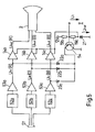
- Fig. 1 shows a circuit for controlling a CRT as it is known from US 6,057,883.
- the known circuit which is designated as a whole with the reference symbol 1 has three outputs connected to the electron guns of a CRT 2.
- Each output of the control circuit 1 is associated with a video amplifier 3, 4, 5 for each of the primary colours red, green and blue.
- the amplifiers 3, 4, 5 receive colour input signals U in (R), U in (G), U in (B) to generate colour output signals U out (R), U out (G), U out (B).
- the outputs of the amplifiers are each connected to the cathode of a diode 6, 7, 8, respectively.
- the diodes are biased in forward direction by an external voltage U 1 .
- the colour output signals U out (R), U out (G), U out (B) are prevented from falling below the external voltage U 1 .
- the known circuit avoids smears as described in the introduction.
- Fig. 2 displays an embodiment of the inventive circuit.
- the circuit designated as a whole with the reference symbol 10 performs the amplification of a colour input signal U in (R) to generate a colour output signal U out (R). This is similar to the function of the amplifier 3 shown in Fig. 1.
- the circuit 10 receives at input terminal 11 the colour input signal U in (R), which is coupled via a voltage divider composed of resistors 12 and 13 to the inverting input of amplifier 14.
- the amplifier generates the colour output signal U out (R) supplied to the output terminal 16 and coupled back by resistor 17 to the inverting input of the amplifier 14.
- the non-inverting input of the amplifier 14 is supplied with a reference voltage U ref .
- the reference voltage U ref is supplied and stabilized by a series connection of a first voltage source 18, resistor 19 and Zener diode 21.
- the first voltage source 18 provides essentially 12 V and the reference voltage is essentially equal to 3 V.
- the input terminal 11 is further connected to the anode of a diode 22.
- the diode 22 is biased in reverse direction by a voltage U 1 provided by a second voltage source 23.
- the voltage U 1 is about 4.9 V and the turn-on voltage U d of the diode 22 is 0.6 V.
- the diode 22 becomes conducting when the colour input signal U in (R) exceeds 5.5 V and hence effectively limits the maximum level of the input signal.
- the dimensions of the circuit and in particular the amount of feedback are selected such that the amplifier 14 does not reach saturation. Smear effects on the screen are consequently avoided.
- Fig. 3 the effect of the inventive circuit on the input signal U in (R) is visualized.
- the maximal amplitude of the input signal U in (R) is limited to a threshold voltage of U 1 + U d , which is the bias voltage of the second voltage source 23 and the turn-on voltage of the diode 22.
- the threshold voltage is represented by a dashed line in Fig. 2.
- the curve the input signal would follow without limitation by diode 22 is indicated with a dotted line. It is understood that the input signal U in (R) is representative for all other input signals U in (G) , U in (B) .
- Fig. 4 shows a second embodiment of the inventive circuit, which is identified as a whole with the reference symbol 40. Corresponding components and elements are identified with the same or corresponding reference symbols.
- the voltage source 18 is also used to supply the bias voltage U 1 for the diode 22.
- the cathode of diode 22 is tapped to a series connection of resistors 19a, 19b essentially replacing the resistor 19 of circuit 10.
- the resistors 19a and 19b are selected such that diode 22 is biased in reverse direction by a voltage U 1 , similar to the configuration in Fig. 2.
- the limiting voltage in this embodiment is derived from the same source 18 that supplies the reference voltage.
- the voltage source 18 provides a higher than nominal voltage both the reference voltage U ref and the bias voltage U 1 are increasing.
- a higher reference voltage U ref reduces the output signal U out (R) for a given input signal U in (R).
- the input signal U in (R) exceeds the threshold voltage U 1 und U d the increased U 1, i.e. higher than its nominal value, allows a higher maximum input signal level.
- the two effects are counteracting and the tolerance of the output signal level is reduced compared to the circuit 10.
- Fig. 5 displays a further schematic diagram of the inventive circuit emphasizing some other aspects of the invention not shown in Fig. 2 and Fig. 4, but suppressing some details already described there.
- the video signals for the three primary colours are received from a video processing board (not shown in the drawing) at connector 51.
- the signals of the primary colours are processed individually in delay lines 52a, 52b, 52c and preamplifiers 53a, 53b, 53c.
- the output signals of the preamplifiers provide the video input signals U in (R), U in (G), U in (B) for the video end stages 14a, 14b, 14c at their respective inverting inputs.
- the video end stage is the integrated circuit TDA 6111 Q manufactured by Philips.
- the non-inverting input of the video end stages is supplied with a reference voltage U ref .
- each video end stage 14a, 14b, 14c is connected with the anode of a diode 22a, 22b, 22c, respectively.
- the cathodes of the diodes 22a, 22b, 22c are connected in parallel with the emitter of a pnp transistor 54.
- the base of the transistor 54 is biased with a positive voltage U 1 taken from a tap of the series connection of resistors 19a, 19b, similar to the configuration displayed in Fig. 4.
- the video input voltages Ui n (R), U in (G), U in (B) are limited to a maximum value equal to U 1 + U be + U d , .
- U d is the diode voltage of the diodes 22a, 22b, 22c.
- transistor 54 is not absolutely necessary. It would also be possible to connect the cathodes of the diodes 22a, 22b and 22c directly to the tap of the voltage divider 19a, 19b. In order to keep the same threshold voltage it would only be necessary to adapt the values of resistors 19a, 19b to compensate for the absence of the base-emitter voltage U be . However, this simplification of the circuit would sacrifice the decoupling effect described above.
Landscapes
- Engineering & Computer Science (AREA)
- Multimedia (AREA)
- Signal Processing (AREA)
- Processing Of Color Television Signals (AREA)
- Video Image Reproduction Devices For Color Tv Systems (AREA)
Priority Applications (8)
| Application Number | Priority Date | Filing Date | Title |
|---|---|---|---|
| EP01124111A EP1304886A1 (de) | 2001-10-10 | 2001-10-10 | Unterdrückung von Sättigung im Signalverstärker einer Kathodenstrahlröhre |
| KR1020020056355A KR20030030856A (ko) | 2001-10-10 | 2002-09-17 | Crt 출력 증폭기의 포화 억제 |
| EP20020292408 EP1317149A2 (de) | 2001-10-10 | 2002-09-30 | Verhindern von Sättigung in einem Ausgangsverstärker einer Kathodenstrahlröhre |
| MXPA02009690A MXPA02009690A (es) | 2001-10-10 | 2002-10-01 | Supresion de saturacion de amplificadores de salida de crt.. |
| US10/262,790 US6703802B2 (en) | 2001-10-10 | 2002-10-02 | Saturation suppression of CRT output amplifiers |
| MYPI20023748A MY171047A (en) | 2001-10-10 | 2002-10-08 | Saturation suppression of crt output amplifiers |
| JP2002297648A JP2003189319A (ja) | 2001-10-10 | 2002-10-10 | 陰極線管を制御するための回路及びテレビジョン受信機 |
| CN02144354A CN1413032A (zh) | 2001-10-10 | 2002-10-10 | 阴极射线管输出放大器的饱和抑制 |
Applications Claiming Priority (1)
| Application Number | Priority Date | Filing Date | Title |
|---|---|---|---|
| EP01124111A EP1304886A1 (de) | 2001-10-10 | 2001-10-10 | Unterdrückung von Sättigung im Signalverstärker einer Kathodenstrahlröhre |
Publications (1)
| Publication Number | Publication Date |
|---|---|
| EP1304886A1 true EP1304886A1 (de) | 2003-04-23 |
Family
ID=8178907
Family Applications (1)
| Application Number | Title | Priority Date | Filing Date |
|---|---|---|---|
| EP01124111A Withdrawn EP1304886A1 (de) | 2001-10-10 | 2001-10-10 | Unterdrückung von Sättigung im Signalverstärker einer Kathodenstrahlröhre |
Country Status (7)
| Country | Link |
|---|---|
| US (1) | US6703802B2 (de) |
| EP (1) | EP1304886A1 (de) |
| JP (1) | JP2003189319A (de) |
| KR (1) | KR20030030856A (de) |
| CN (1) | CN1413032A (de) |
| MX (1) | MXPA02009690A (de) |
| MY (1) | MY171047A (de) |
Families Citing this family (2)
| Publication number | Priority date | Publication date | Assignee | Title |
|---|---|---|---|---|
| CN101119434B (zh) * | 2006-08-04 | 2010-05-12 | 深圳Tcl新技术有限公司 | 控制阴极射线管的电路及方法 |
| CN108141185B (zh) * | 2015-10-05 | 2021-08-03 | 瑞典爱立信有限公司 | 包括限幅的放大装置 |
Citations (2)
| Publication number | Priority date | Publication date | Assignee | Title |
|---|---|---|---|---|
| JPS5520051A (en) * | 1978-07-29 | 1980-02-13 | Iwatsu Electric Co Ltd | Amplifier |
| JPH0371784A (ja) * | 1989-08-11 | 1991-03-27 | Hitachi Ltd | 映像出力回路 |
Family Cites Families (4)
| Publication number | Priority date | Publication date | Assignee | Title |
|---|---|---|---|---|
| JPS5553978A (en) * | 1978-10-17 | 1980-04-19 | Sony Corp | Automatic luminance adjusting device for television picture receiver |
| US5455635A (en) * | 1994-04-28 | 1995-10-03 | Rca Thomson Licensing Corporation | Kinescope driver with gamma correction and brightness dependent capacitor coupling |
| DE19744902A1 (de) * | 1996-11-26 | 1998-05-28 | Thomson Brandt Gmbh | Schaltung zur Steuerung der Bildröhre in einem Fernsehempfänger |
| JP2000022988A (ja) * | 1998-07-06 | 2000-01-21 | Sony Corp | ガンマ補正回路 |
-
2001
- 2001-10-10 EP EP01124111A patent/EP1304886A1/de not_active Withdrawn
-
2002
- 2002-09-17 KR KR1020020056355A patent/KR20030030856A/ko not_active Withdrawn
- 2002-10-01 MX MXPA02009690A patent/MXPA02009690A/es active IP Right Grant
- 2002-10-02 US US10/262,790 patent/US6703802B2/en not_active Expired - Fee Related
- 2002-10-08 MY MYPI20023748A patent/MY171047A/en unknown
- 2002-10-10 CN CN02144354A patent/CN1413032A/zh active Pending
- 2002-10-10 JP JP2002297648A patent/JP2003189319A/ja active Pending
Patent Citations (2)
| Publication number | Priority date | Publication date | Assignee | Title |
|---|---|---|---|---|
| JPS5520051A (en) * | 1978-07-29 | 1980-02-13 | Iwatsu Electric Co Ltd | Amplifier |
| JPH0371784A (ja) * | 1989-08-11 | 1991-03-27 | Hitachi Ltd | 映像出力回路 |
Non-Patent Citations (2)
| Title |
|---|
| PATENT ABSTRACTS OF JAPAN vol. 004, no. 048 (E - 006) 12 April 1980 (1980-04-12) * |
| PATENT ABSTRACTS OF JAPAN vol. 015, no. 236 (E - 1078) 18 June 1991 (1991-06-18) * |
Also Published As
| Publication number | Publication date |
|---|---|
| US20030067272A1 (en) | 2003-04-10 |
| MY171047A (en) | 2019-09-23 |
| KR20030030856A (ko) | 2003-04-18 |
| US6703802B2 (en) | 2004-03-09 |
| JP2003189319A (ja) | 2003-07-04 |
| MXPA02009690A (es) | 2005-02-17 |
| CN1413032A (zh) | 2003-04-23 |
Similar Documents
| Publication | Publication Date | Title |
|---|---|---|
| EP0613307A1 (de) | Schaltung zur Kompensation der Abschwächung des blauen Phosphors bei hohem Anregungspegel in einem Projektionsfernsehsystem | |
| US5083198A (en) | Nonlinear RGB video signal processing | |
| EP0700208B1 (de) | Schaltungen zum Begrenzen der automatischen Helligkeits- und Kontraststeuerung und Prozessor zum Verarbeiten der Luminanz- und Farbdifferenzsignale und Videoanzeigegerät mit solchen Schaltungen | |
| RU2183386C2 (ru) | Устройство возбуждения кинескопа с гамма-коррекцией | |
| KR950006235B1 (ko) | 텔레비젼 수상기용 명도 제어회로 | |
| US6703802B2 (en) | Saturation suppression of CRT output amplifiers | |
| KR100228607B1 (ko) | 칼러 화상 표시 장치 및 칼러 카메라 | |
| US4346399A (en) | Color temperature control circuit | |
| KR100338236B1 (ko) | 비디오신호처리장치 | |
| EP1317149A2 (de) | Verhindern von Sättigung in einem Ausgangsverstärker einer Kathodenstrahlröhre | |
| US5726540A (en) | Transient enhancement circuit for CRT amplifier | |
| AU648276B2 (en) | Nonlinear RGB video signal processing | |
| US5644360A (en) | Circuit for compensating the blue phosphor roll off at high drive levels in a projection television system | |
| GB2217156A (en) | Anti-zero biasing clamp | |
| US6057883A (en) | Circuit for controlling the picture tube in a television receiver | |
| KR100214634B1 (ko) | 프로젝션 티브이의 b색 감마보정 회로 | |
| KR100311767B1 (ko) | 키네스코프구동용증폭기장치 | |
| KR100339060B1 (ko) | 감마보정을갖는키네스코프구동장치 | |
| KR100191319B1 (ko) | 어두운화면의 화이트밸런스조정회로 | |
| KR860001696Y1 (ko) | 모니터를 위한 컬러 tv의 잡음 방지회로 | |
| US20030030726A1 (en) | Cathode current limiting circuit for projection television display systems | |
| KR20000010319U (ko) | 화질 보상회로 | |
| JPH09284799A (ja) | ビデオプロジェクタ用のホワイトバランス補正装置 | |
| JPH11261847A (ja) | 映像信号処理回路 | |
| CN101119434A (zh) | 控制阴极射线管的电路及方法 |
Legal Events
| Date | Code | Title | Description |
|---|---|---|---|
| PUAI | Public reference made under article 153(3) epc to a published international application that has entered the european phase |
Free format text: ORIGINAL CODE: 0009012 |
|
| AK | Designated contracting states |
Designated state(s): AT BE CH CY DE DK ES FI FR GB GR IE IT LI LU MC NL PT SE TR |
|
| AX | Request for extension of the european patent |
Extension state: AL LT LV MK RO SI |
|
| AKX | Designation fees paid | ||
| REG | Reference to a national code |
Ref country code: DE Ref legal event code: 8566 |
|
| STAA | Information on the status of an ep patent application or granted ep patent |
Free format text: STATUS: THE APPLICATION IS DEEMED TO BE WITHDRAWN |
|
| 18D | Application deemed to be withdrawn |
Effective date: 20031024 |