EP1307078A2 - Hochfrequenzschaltungsmodul - Google Patents
Hochfrequenzschaltungsmodul Download PDFInfo
- Publication number
- EP1307078A2 EP1307078A2 EP02003265A EP02003265A EP1307078A2 EP 1307078 A2 EP1307078 A2 EP 1307078A2 EP 02003265 A EP02003265 A EP 02003265A EP 02003265 A EP02003265 A EP 02003265A EP 1307078 A2 EP1307078 A2 EP 1307078A2
- Authority
- EP
- European Patent Office
- Prior art keywords
- layer
- dielectric substrate
- high frequency
- multilayer dielectric
- metallic
- Prior art date
- Legal status (The legal status is an assumption and is not a legal conclusion. Google has not performed a legal analysis and makes no representation as to the accuracy of the status listed.)
- Granted
Links
Images


Classifications
-
- H—ELECTRICITY
- H05—ELECTRIC TECHNIQUES NOT OTHERWISE PROVIDED FOR
- H05K—PRINTED CIRCUITS; CASINGS OR CONSTRUCTIONAL DETAILS OF ELECTRIC APPARATUS; MANUFACTURE OF ASSEMBLAGES OF ELECTRICAL COMPONENTS
- H05K1/00—Printed circuits
- H05K1/02—Details
- H05K1/0213—Electrical arrangements not otherwise provided for
- H05K1/0216—Reduction of cross-talk, noise or electromagnetic interference
- H05K1/0218—Reduction of cross-talk, noise or electromagnetic interference by printed shielding conductors, ground planes or power plane
- H05K1/0219—Printed shielding conductors for shielding around or between signal conductors, e.g. coplanar or coaxial printed shielding conductors
- H05K1/0222—Printed shielding conductors for shielding around or between signal conductors, e.g. coplanar or coaxial printed shielding conductors for shielding around a single via or around a group of vias, e.g. coaxial vias or vias surrounded by a grounded via fence
-
- H—ELECTRICITY
- H01—ELECTRIC ELEMENTS
- H01P—WAVEGUIDES; RESONATORS, LINES, OR OTHER DEVICES OF THE WAVEGUIDE TYPE
- H01P1/00—Auxiliary devices
- H01P1/04—Fixed joints
- H01P1/047—Strip line joints
-
- H—ELECTRICITY
- H01—ELECTRIC ELEMENTS
- H01Q—ANTENNAS, i.e. RADIO AERIALS
- H01Q1/00—Details of, or arrangements associated with, antennas
- H01Q1/27—Adaptation for use in or on movable bodies
- H01Q1/32—Adaptation for use in or on road or rail vehicles
- H01Q1/3208—Adaptation for use in or on road or rail vehicles characterised by the application wherein the antenna is used
- H01Q1/3233—Adaptation for use in or on road or rail vehicles characterised by the application wherein the antenna is used particular used as part of a sensor or in a security system, e.g. for automotive radar, navigation systems
-
- H—ELECTRICITY
- H01—ELECTRIC ELEMENTS
- H01Q—ANTENNAS, i.e. RADIO AERIALS
- H01Q21/00—Antenna arrays or systems
- H01Q21/0087—Apparatus or processes specially adapted for manufacturing antenna arrays
-
- H—ELECTRICITY
- H01—ELECTRIC ELEMENTS
- H01Q—ANTENNAS, i.e. RADIO AERIALS
- H01Q23/00—Antennas with active circuits or circuit elements integrated within them or attached to them
-
- H—ELECTRICITY
- H01—ELECTRIC ELEMENTS
- H01Q—ANTENNAS, i.e. RADIO AERIALS
- H01Q9/00—Electrically-short antennas having dimensions not more than twice the operating wavelength and consisting of conductive active radiating elements
- H01Q9/04—Resonant antennas
- H01Q9/0407—Substantially flat resonant element parallel to ground plane, e.g. patch antenna
-
- H—ELECTRICITY
- H10—SEMICONDUCTOR DEVICES; ELECTRIC SOLID-STATE DEVICES NOT OTHERWISE PROVIDED FOR
- H10W—GENERIC PACKAGES, INTERCONNECTIONS, CONNECTORS OR OTHER CONSTRUCTIONAL DETAILS OF DEVICES COVERED BY CLASS H10
- H10W42/00—Arrangements for protection of devices
- H10W42/20—Arrangements for protection of devices protecting against electromagnetic or particle radiation, e.g. light, X-rays, gamma-rays or electrons
-
- H—ELECTRICITY
- H10—SEMICONDUCTOR DEVICES; ELECTRIC SOLID-STATE DEVICES NOT OTHERWISE PROVIDED FOR
- H10W—GENERIC PACKAGES, INTERCONNECTIONS, CONNECTORS OR OTHER CONSTRUCTIONAL DETAILS OF DEVICES COVERED BY CLASS H10
- H10W44/00—Electrical arrangements for controlling or matching impedance
- H10W44/20—Electrical arrangements for controlling or matching impedance at high-frequency [HF] or radio frequency [RF]
-
- G—PHYSICS
- G01—MEASURING; TESTING
- G01S—RADIO DIRECTION-FINDING; RADIO NAVIGATION; DETERMINING DISTANCE OR VELOCITY BY USE OF RADIO WAVES; LOCATING OR PRESENCE-DETECTING BY USE OF THE REFLECTION OR RERADIATION OF RADIO WAVES; ANALOGOUS ARRANGEMENTS USING OTHER WAVES
- G01S13/00—Systems using the reflection or reradiation of radio waves, e.g. radar systems; Analogous systems using reflection or reradiation of waves whose nature or wavelength is irrelevant or unspecified
- G01S13/88—Radar or analogous systems specially adapted for specific applications
- G01S13/93—Radar or analogous systems specially adapted for specific applications for anti-collision purposes
- G01S13/931—Radar or analogous systems specially adapted for specific applications for anti-collision purposes of land vehicles
-
- G—PHYSICS
- G01—MEASURING; TESTING
- G01S—RADIO DIRECTION-FINDING; RADIO NAVIGATION; DETERMINING DISTANCE OR VELOCITY BY USE OF RADIO WAVES; LOCATING OR PRESENCE-DETECTING BY USE OF THE REFLECTION OR RERADIATION OF RADIO WAVES; ANALOGOUS ARRANGEMENTS USING OTHER WAVES
- G01S7/00—Details of systems according to groups G01S13/00, G01S15/00, G01S17/00
- G01S7/02—Details of systems according to groups G01S13/00, G01S15/00, G01S17/00 of systems according to group G01S13/00
- G01S7/027—Constructional details of housings, e.g. form, type, material or ruggedness
- G01S7/028—Miniaturisation, e.g. surface mounted device [SMD] packaging or housings
-
- G—PHYSICS
- G01—MEASURING; TESTING
- G01S—RADIO DIRECTION-FINDING; RADIO NAVIGATION; DETERMINING DISTANCE OR VELOCITY BY USE OF RADIO WAVES; LOCATING OR PRESENCE-DETECTING BY USE OF THE REFLECTION OR RERADIATION OF RADIO WAVES; ANALOGOUS ARRANGEMENTS USING OTHER WAVES
- G01S7/00—Details of systems according to groups G01S13/00, G01S15/00, G01S17/00
- G01S7/02—Details of systems according to groups G01S13/00, G01S15/00, G01S17/00 of systems according to group G01S13/00
- G01S7/03—Details of HF subsystems specially adapted therefor, e.g. common to transmitter and receiver
- G01S7/032—Constructional details for solid-state radar subsystems
-
- H—ELECTRICITY
- H05—ELECTRIC TECHNIQUES NOT OTHERWISE PROVIDED FOR
- H05K—PRINTED CIRCUITS; CASINGS OR CONSTRUCTIONAL DETAILS OF ELECTRIC APPARATUS; MANUFACTURE OF ASSEMBLAGES OF ELECTRICAL COMPONENTS
- H05K1/00—Printed circuits
- H05K1/02—Details
- H05K1/0213—Electrical arrangements not otherwise provided for
- H05K1/0216—Reduction of cross-talk, noise or electromagnetic interference
- H05K1/0218—Reduction of cross-talk, noise or electromagnetic interference by printed shielding conductors, ground planes or power plane
- H05K1/0219—Printed shielding conductors for shielding around or between signal conductors, e.g. coplanar or coaxial printed shielding conductors
- H05K1/0221—Coaxially shielded signal lines comprising a continuous shielding layer partially or wholly surrounding the signal lines
-
- H—ELECTRICITY
- H05—ELECTRIC TECHNIQUES NOT OTHERWISE PROVIDED FOR
- H05K—PRINTED CIRCUITS; CASINGS OR CONSTRUCTIONAL DETAILS OF ELECTRIC APPARATUS; MANUFACTURE OF ASSEMBLAGES OF ELECTRICAL COMPONENTS
- H05K1/00—Printed circuits
- H05K1/02—Details
- H05K1/0213—Electrical arrangements not otherwise provided for
- H05K1/0237—High frequency adaptations
- H05K1/0243—Printed circuits associated with mounted high frequency components
-
- H—ELECTRICITY
- H05—ELECTRIC TECHNIQUES NOT OTHERWISE PROVIDED FOR
- H05K—PRINTED CIRCUITS; CASINGS OR CONSTRUCTIONAL DETAILS OF ELECTRIC APPARATUS; MANUFACTURE OF ASSEMBLAGES OF ELECTRICAL COMPONENTS
- H05K1/00—Printed circuits
- H05K1/02—Details
- H05K1/0296—Conductive pattern lay-out details not covered by sub groups H05K1/02 - H05K1/0295
- H05K1/0298—Multilayer circuits
-
- H—ELECTRICITY
- H05—ELECTRIC TECHNIQUES NOT OTHERWISE PROVIDED FOR
- H05K—PRINTED CIRCUITS; CASINGS OR CONSTRUCTIONAL DETAILS OF ELECTRIC APPARATUS; MANUFACTURE OF ASSEMBLAGES OF ELECTRICAL COMPONENTS
- H05K1/00—Printed circuits
- H05K1/02—Details
- H05K1/03—Use of materials for the substrate
- H05K1/0306—Inorganic insulating substrates, e.g. ceramic, glass
-
- H—ELECTRICITY
- H05—ELECTRIC TECHNIQUES NOT OTHERWISE PROVIDED FOR
- H05K—PRINTED CIRCUITS; CASINGS OR CONSTRUCTIONAL DETAILS OF ELECTRIC APPARATUS; MANUFACTURE OF ASSEMBLAGES OF ELECTRICAL COMPONENTS
- H05K1/00—Printed circuits
- H05K1/02—Details
- H05K1/11—Printed elements for providing electric connections to or between printed circuits
- H05K1/115—Via connections; Lands around holes or via connections
- H05K1/116—Lands, clearance holes or other lay-out details concerning the surrounding of a via
-
- H—ELECTRICITY
- H05—ELECTRIC TECHNIQUES NOT OTHERWISE PROVIDED FOR
- H05K—PRINTED CIRCUITS; CASINGS OR CONSTRUCTIONAL DETAILS OF ELECTRIC APPARATUS; MANUFACTURE OF ASSEMBLAGES OF ELECTRICAL COMPONENTS
- H05K2201/00—Indexing scheme relating to printed circuits covered by H05K1/00
- H05K2201/09—Shape and layout
- H05K2201/09209—Shape and layout details of conductors
- H05K2201/095—Conductive through-holes or vias
- H05K2201/09618—Via fence, i.e. one-dimensional array of vias
-
- H—ELECTRICITY
- H05—ELECTRIC TECHNIQUES NOT OTHERWISE PROVIDED FOR
- H05K—PRINTED CIRCUITS; CASINGS OR CONSTRUCTIONAL DETAILS OF ELECTRIC APPARATUS; MANUFACTURE OF ASSEMBLAGES OF ELECTRICAL COMPONENTS
- H05K2201/00—Indexing scheme relating to printed circuits covered by H05K1/00
- H05K2201/09—Shape and layout
- H05K2201/09209—Shape and layout details of conductors
- H05K2201/09654—Shape and layout details of conductors covering at least two types of conductors provided for in H05K2201/09218 - H05K2201/095
- H05K2201/09781—Dummy conductors, i.e. not used for normal transport of current; Dummy electrodes of components
-
- H—ELECTRICITY
- H05—ELECTRIC TECHNIQUES NOT OTHERWISE PROVIDED FOR
- H05K—PRINTED CIRCUITS; CASINGS OR CONSTRUCTIONAL DETAILS OF ELECTRIC APPARATUS; MANUFACTURE OF ASSEMBLAGES OF ELECTRICAL COMPONENTS
- H05K2201/00—Indexing scheme relating to printed circuits covered by H05K1/00
- H05K2201/09—Shape and layout
- H05K2201/09209—Shape and layout details of conductors
- H05K2201/09654—Shape and layout details of conductors covering at least two types of conductors provided for in H05K2201/09218 - H05K2201/095
- H05K2201/09809—Coaxial layout
-
- H—ELECTRICITY
- H05—ELECTRIC TECHNIQUES NOT OTHERWISE PROVIDED FOR
- H05K—PRINTED CIRCUITS; CASINGS OR CONSTRUCTIONAL DETAILS OF ELECTRIC APPARATUS; MANUFACTURE OF ASSEMBLAGES OF ELECTRICAL COMPONENTS
- H05K3/00—Apparatus or processes for manufacturing printed circuits
- H05K3/40—Forming printed elements for providing electric connections to or between printed circuits
- H05K3/42—Plated through-holes or plated via connections
- H05K3/429—Plated through-holes specially for multilayer circuits, e.g. having connections to inner circuit layers
-
- H—ELECTRICITY
- H05—ELECTRIC TECHNIQUES NOT OTHERWISE PROVIDED FOR
- H05K—PRINTED CIRCUITS; CASINGS OR CONSTRUCTIONAL DETAILS OF ELECTRIC APPARATUS; MANUFACTURE OF ASSEMBLAGES OF ELECTRICAL COMPONENTS
- H05K3/00—Apparatus or processes for manufacturing printed circuits
- H05K3/46—Manufacturing multilayer circuits
- H05K3/4611—Manufacturing multilayer circuits by laminating two or more circuit boards
- H05K3/4626—Manufacturing multilayer circuits by laminating two or more circuit boards characterised by the insulating layers or materials
- H05K3/4629—Manufacturing multilayer circuits by laminating two or more circuit boards characterised by the insulating layers or materials laminating inorganic sheets comprising printed circuits, e.g. green ceramic sheets
-
- H—ELECTRICITY
- H10—SEMICONDUCTOR DEVICES; ELECTRIC SOLID-STATE DEVICES NOT OTHERWISE PROVIDED FOR
- H10W—GENERIC PACKAGES, INTERCONNECTIONS, CONNECTORS OR OTHER CONSTRUCTIONAL DETAILS OF DEVICES COVERED BY CLASS H10
- H10W44/00—Electrical arrangements for controlling or matching impedance
- H10W44/20—Electrical arrangements for controlling or matching impedance at high-frequency [HF] or radio frequency [RF]
- H10W44/203—Electrical connections
- H10W44/209—Vertical interconnections, e.g. vias
-
- H—ELECTRICITY
- H10—SEMICONDUCTOR DEVICES; ELECTRIC SOLID-STATE DEVICES NOT OTHERWISE PROVIDED FOR
- H10W—GENERIC PACKAGES, INTERCONNECTIONS, CONNECTORS OR OTHER CONSTRUCTIONAL DETAILS OF DEVICES COVERED BY CLASS H10
- H10W44/00—Electrical arrangements for controlling or matching impedance
- H10W44/20—Electrical arrangements for controlling or matching impedance at high-frequency [HF] or radio frequency [RF]
- H10W44/203—Electrical connections
- H10W44/216—Waveguides, e.g. strip lines
-
- H—ELECTRICITY
- H10—SEMICONDUCTOR DEVICES; ELECTRIC SOLID-STATE DEVICES NOT OTHERWISE PROVIDED FOR
- H10W—GENERIC PACKAGES, INTERCONNECTIONS, CONNECTORS OR OTHER CONSTRUCTIONAL DETAILS OF DEVICES COVERED BY CLASS H10
- H10W44/00—Electrical arrangements for controlling or matching impedance
- H10W44/20—Electrical arrangements for controlling or matching impedance at high-frequency [HF] or radio frequency [RF]
- H10W44/241—Electrical arrangements for controlling or matching impedance at high-frequency [HF] or radio frequency [RF] for passive devices or passive elements
- H10W44/248—Electrical arrangements for controlling or matching impedance at high-frequency [HF] or radio frequency [RF] for passive devices or passive elements for antennas
-
- H—ELECTRICITY
- H10—SEMICONDUCTOR DEVICES; ELECTRIC SOLID-STATE DEVICES NOT OTHERWISE PROVIDED FOR
- H10W—GENERIC PACKAGES, INTERCONNECTIONS, CONNECTORS OR OTHER CONSTRUCTIONAL DETAILS OF DEVICES COVERED BY CLASS H10
- H10W44/00—Electrical arrangements for controlling or matching impedance
- H10W44/20—Electrical arrangements for controlling or matching impedance at high-frequency [HF] or radio frequency [RF]
- H10W44/255—Electrical arrangements for controlling or matching impedance at high-frequency [HF] or radio frequency [RF] for operation at multiple different frequencies
-
- H—ELECTRICITY
- H10—SEMICONDUCTOR DEVICES; ELECTRIC SOLID-STATE DEVICES NOT OTHERWISE PROVIDED FOR
- H10W—GENERIC PACKAGES, INTERCONNECTIONS, CONNECTORS OR OTHER CONSTRUCTIONAL DETAILS OF DEVICES COVERED BY CLASS H10
- H10W70/00—Package substrates; Interposers; Redistribution layers [RDL]
- H10W70/60—Insulating or insulated package substrates; Interposers; Redistribution layers
- H10W70/67—Insulating or insulated package substrates; Interposers; Redistribution layers characterised by their insulating layers or insulating parts
- H10W70/68—Shapes or dispositions thereof
- H10W70/682—Shapes or dispositions thereof comprising holes having chips therein
-
- H—ELECTRICITY
- H10—SEMICONDUCTOR DEVICES; ELECTRIC SOLID-STATE DEVICES NOT OTHERWISE PROVIDED FOR
- H10W—GENERIC PACKAGES, INTERCONNECTIONS, CONNECTORS OR OTHER CONSTRUCTIONAL DETAILS OF DEVICES COVERED BY CLASS H10
- H10W70/00—Package substrates; Interposers; Redistribution layers [RDL]
- H10W70/60—Insulating or insulated package substrates; Interposers; Redistribution layers
- H10W70/67—Insulating or insulated package substrates; Interposers; Redistribution layers characterised by their insulating layers or insulating parts
- H10W70/68—Shapes or dispositions thereof
- H10W70/685—Shapes or dispositions thereof comprising multiple insulating layers
-
- H—ELECTRICITY
- H10—SEMICONDUCTOR DEVICES; ELECTRIC SOLID-STATE DEVICES NOT OTHERWISE PROVIDED FOR
- H10W—GENERIC PACKAGES, INTERCONNECTIONS, CONNECTORS OR OTHER CONSTRUCTIONAL DETAILS OF DEVICES COVERED BY CLASS H10
- H10W72/00—Interconnections or connectors in packages
- H10W72/071—Connecting or disconnecting
- H10W72/075—Connecting or disconnecting of bond wires
-
- H—ELECTRICITY
- H10—SEMICONDUCTOR DEVICES; ELECTRIC SOLID-STATE DEVICES NOT OTHERWISE PROVIDED FOR
- H10W—GENERIC PACKAGES, INTERCONNECTIONS, CONNECTORS OR OTHER CONSTRUCTIONAL DETAILS OF DEVICES COVERED BY CLASS H10
- H10W72/00—Interconnections or connectors in packages
- H10W72/50—Bond wires
- H10W72/551—Materials of bond wires
-
- H—ELECTRICITY
- H10—SEMICONDUCTOR DEVICES; ELECTRIC SOLID-STATE DEVICES NOT OTHERWISE PROVIDED FOR
- H10W—GENERIC PACKAGES, INTERCONNECTIONS, CONNECTORS OR OTHER CONSTRUCTIONAL DETAILS OF DEVICES COVERED BY CLASS H10
- H10W72/00—Interconnections or connectors in packages
- H10W72/90—Bond pads, in general
- H10W72/951—Materials of bond pads
-
- H—ELECTRICITY
- H10—SEMICONDUCTOR DEVICES; ELECTRIC SOLID-STATE DEVICES NOT OTHERWISE PROVIDED FOR
- H10W—GENERIC PACKAGES, INTERCONNECTIONS, CONNECTORS OR OTHER CONSTRUCTIONAL DETAILS OF DEVICES COVERED BY CLASS H10
- H10W90/00—Package configurations
- H10W90/701—Package configurations characterised by the relative positions of pads or connectors relative to package parts
- H10W90/751—Package configurations characterised by the relative positions of pads or connectors relative to package parts of bond wires
- H10W90/754—Package configurations characterised by the relative positions of pads or connectors relative to package parts of bond wires between a chip and a stacked insulating package substrate, interposer or RDL
Definitions
- the present invention relates to a high frequency circuit module and, more specifically, to a high frequency circuit module in which a high frequency circuit part such as a monolithic microwave integrated circuit (hereinbelow, called an MMIC) and an antenna are provided on the surface and the rear face, respectively, of a multilayer dielectric substrate. More particularly, the invention relates to a high frequency circuit module suitable for an automotive radar module using millimeter waves.
- a high frequency circuit part such as a monolithic microwave integrated circuit (hereinbelow, called an MMIC) and an antenna are provided on the surface and the rear face, respectively, of a multilayer dielectric substrate.
- MMIC monolithic microwave integrated circuit
- the invention relates to a high frequency circuit module suitable for an automotive radar module using millimeter waves.
- ITS intelligent transport system
- a high frequency circuit module adapted to the automotive radar, a high frequency circuit module in which an antenna and an MMIC are provided on the surface and rear face, respectively, of a multilayer dielectric substrate having therein metallic layers is known
- an antenna 28 and an MMIC 29 are provided, respectively.
- microstrip lines 34 and 35 and electro-magnetic coupling slots 36 and 37 are used.
- Techniques using electro-magnetic coupling slots of this kind are disclosed in Japanese Unexamined Patent Application Nos. 9-237867 and 8-250913.
- a microstrip line having a length of around ⁇ /2 remains between the slots and works as a resonator.
- the mounting method using the electro-magnetic coupling slots needs a mounting area having the distance of 2 ⁇ or longer between the slots, and layout of the upper and lower electronic parts has to be considered so as not to cause interference with the transfer mode of the slot coupling part.
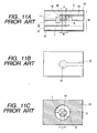
- connection between a plurality of conductive layers 31 and 33 in the multilayer dielectric substrate 38 having the plurality of conductive layers 30 to 33 and 39 is realized by a via satisfying the condition of (R ⁇ r)/(2 ⁇ h) ⁇ L ⁇ (5 ⁇ R ⁇ r)/h (where R, r, and L denote sizes shown in Fig. 11C and h denotes the distance between the conductive layers).
- R, r, and L denote sizes shown in Fig. 11C and h denotes the distance between the conductive layers.
- a technique which does not use a dielectric multilayer substrate as shown in Fig. 12 (conventional technique 3), there is a technique in which an MMIC 43 and an antenna 44 are provided on the surface and rear face, respectively, of a metal base plate 42, and a coaxial structure 45 formed in the base plate 42 is used to connection the MMIC 43 and antenna 44.
- the RF circuit substrate including the MMIC 43 and the antenna are connected to each other via the coaxial structure, so that a thin, small millimeter wave radar can be relatively easily produced.
- reference numerals 46, 47, 48, 49, 50 and 51 denote a circuit substrate, an insulating material, an outer terminal, an insulating material, a bonding wire, and a transmission/reception circuit cover, respectively.
- the conventional techniques have problems with respect to easiness in manufacture, manufacturing cost, and circuit characteristics.
- an RF circuit has a hermetic structure of interrupting the outside air. Since the transmission loss in the millimeter wave band is much larger as compared with that in a microwave band, the transmission line has to be designed to be as short as possible. Although the line length can be shortened by mounting the RF circuit part on the same face of the substrate as the antenna, it is difficult to mount the RF circuit part and the antenna on the same face due to the limited size of the RF circuit part and the hermetic structure.
- the RF circuit part and the antenna of the millimeter wave radar are mounted on both sides of the mounting substrate so as to be overlapped, and an oscillator and an amplifier of the RF circuit parts have to be disposed so that the transmission line length becomes the shortest.
- the mounting substrate of the millimeter wave band a thin substrate having a dielectric thickness of 0.2 mm or less is used to suppress a transmission line radiation loss. Therefore, the base plate 42 for assuring the mechanical strength is needed as shown in Fig. 12 for the millimeter wave radar. Consequently, the structure whose assembling and processing cost is high has to be employed.
- a both-sided two-layer substrate is generally used to assure the characteristics of the millimeter wave transmission line for an RF circuit.
- a transmission line for a millimeter signal, a power providing line, and a transmission line for a low frequency signal are formed on the same face. Since the high/low frequency signal transmission lines and the power providing line cannot cross each other, aerial wiring such as a bonding wire is required. The higher the frequency of a signal is, the more the signal easily radiates, and it causes a crosstalk in another line. It makes the millimeter waver radar unstable.
- the flexibility of designing of layout of the RF circuit is regulated in the two-layer substrate, reduction in cost by reducing the substrate area of the expensive RF circuit part is limited.
- An object of the invention is therefore to realize a high frequency circuit module in which high frequency circuit parts such as MMICs for millimeter waves and microwave and a plane antenna are mounted on a multilayer dielectric substrate and a loss of energy of electromagnetic waves is reduced, and which can be realized at low cost and, further, to provide a small, thin, and light automotive radar module with high design flexibility.
- a high frequency circuit hereinbelow, called an RF circuit
- RF circuit parts are mounted on both sides of a multilayer dielectric substrate, and transmission lines connecting the RF circuit parts on both sides are constructed by a group of vias having a periodical structure or vias having a coaxial structure extended in the direction perpendicular to the face of the multilayer dielectric substrate.
- the via group having the periodical structure is constructed so that a plurality of vias are distributed around a center conductor at a predetermined interval. Particularly, the interval is equal to or smaller than 1/4 of wavelength of a signal of the transmission line.
- the via having the coaxial structure is formed by a center conductor and a cylindrical conductor surrounding the center conductor and connected to a grounding conductive layer provided in the multilayer dielectric substrate.
- RF circuit parts on one of the faces of the hard multilayer dielectric substrate are MMICs such as an oscillator and an RF circuit part on the other face is an antenna.
- the invention is not limited to an automotive radar module but can be applied to an RF circuit module using microwaves and millimeter waves in which RF circuit parts are mounted on both sides of a hard multilayer dielectric substrate.
- a millimeter wave transmission line extending vertically to a layer with a small transmission loss is provided in a hard multilayer dielectric substrate, and a metal layer for a DC/IF signal is shielded by grounding metal layers in the substrate.
- crosstalk to a DC/IF signal of a millimeter wave signal is lessened, the area occupied by the RF circuits can be reduced by multilayer wiring of the RF circuit, and resistance to distortion and destruction by a mechanical stress moment of the multilayer substrate is improved.
- the surface of the multilayer dielectric substrate is flat and the assembling work is easily made by one-side reflowing, so that a small, thin, and low-cost RF circuit module can be realized.
- the invention is effective to realize an automotive radar module having excellent cost efficiency and resistance to vibration, which is requested to have high performance.
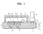
- Fig. 1 is a sectional side view showing the configuration of an example of an RF circuit module according to the invention.
- the RF circuit module is used for an automotive radar using a millimeter wave.
- a hard multilayer dielectric substrate 2 of the embodiment four hard dielectric layers 2-1, 2-2, 2-3, and 2-4 are formed, metallic layers 9, 10, and 11 are formed on the layers 2-2, 2-3, and 2-4, respectively, and a metallic pattern 17 is formed on the top face of the layer 2-1.
- a transmission line such as a microstrip line is formed.
- the metallic layer 10 constructs a power providing line and a low frequency signal transmission line, and the metallic line 11 is used as a grounding metallic layer.
- RF circuit parts 5-1 and 5-2 such as MMICs are mounted on the surface of the hard dielectric layer 2-1.
- a metallic pattern 1 for forming an antenna as one of the RF circuit parts is formed on the outer face (rear face) of the dielectric layer 2-4.
- a millimeter wave transmission line 16 extending perpendicular to the face of the multilayer dielectric substrate 2 is formed as a coupling transmission line.
- the millimeter wave transmission line 16 takes the form of a transmission line using a through via having a periodical structure or a through via having a coaxial structure which will be described hereinlater and transmits a millimeter wave signal between the metallic pattern 1 of the antenna and the RF circuit parts 5.
- the metallic pattern 1 of the antenna is processed so as to be adapted to the shape of a millimeter wave transmission via in the rear face of the RF circuit module.
- the multilayer dielectric substrate 2 On the top face of the multilayer dielectric substrate 2, not only the plurality of MMICs 5-1 and 5-2 but also other RF circuit parts such as a mono layer capacitor 13, a chip part 14, and a metallic pattern constructing a microstrip line are mounted.
- the RF circuit parts are hermetically sealed with a hermetic cap 4, thereby forming an RF circuit module.
- An input/output connector 15 is provided on the outside of the hermetic cap 4 and on the top face of the multilayer dielectric substrate 2.
- the hermetic cap 4 is made of a metal or an insulator which is metal plated.
- the hermetic cap 4 and the hard multilayer dielectric substrate 2 are airtightly sealed with an eutectic solder or the like to suppress deterioration in the temperature and moisture environments of the millimeter wave RF circuit constructed by the millimeter wave MMIC 5 and the like. Since the higher the electromagnetic wave is, the more it easily radiates to the air, particularly to avoid crosstalk in the millimeter wave RF circuit, a wave absorber whose electromagnetic wave absorption amount is 10 dB or more or a projected structure having a projection cycle of ⁇ /2 is provided on the inner face of the hermetic cap 4.
- the millimeter wave MMIC 5 is bare-chip bonded or flip-chip bonded to the surface of the hard multilayer dielectric substrate 2.
- wire bonding can be used for a transmission line of an electric signal.
- Figs. 2A and 2B are diagrams for explaining the configuration of an example of the millimeter wave transmission line (hereinbelow, also called a vertical transmission line) 16 formed in the direction perpendicular to the face of the multilayer dielectric substrate 2 in Fig. 1.
- Figs. 2A and 2B are perspective view and a partial cross section, respectively, of the vertical transmission line 16. Each layer is shown in a square shape for simplicity but actually has a wide width.
- a metallic pattern 17-1 is formed by the surface metallic layer and connected to the MMIC (not shown).
- a microstrip transmission line is formed by the metallic pattern 17-1, the grounding metallic layer 9 as a counter electrode, and the dielectric substrate 2-1 provided between the pattern 17-1 and the layer 9.
- the metallic layer 10 is a metallic pattern of a DC (direct current)/IF (intermediate frequency) signal line, and the metallic layer 11 is a metallic pattern for shielding the DC/IF signal line.
- a cylindrical metallic pattern 18 is used to connect the grounding metal layers 9 and 10 to each other.
- the cylindrical metallic pattern 18 and a center conductor 19 construct a via having the coaxial structure.
- the coaxial structure is formed by sintering the multilayer dielectric substrate 2, irradiating the rear face of the metallic layer 11 with a laser beam to form a hole reaching the metallic layer 9 and after that, performing gold plated filling.
- the via 19 serving as a central conductor and the land pattern 17 in the surface layer are larger than the land patterns of the metallic layers 9 to 11.
- a land less pattern of the metallic layers 9 to 11 is designed to be 1/4 of the wavelength or less, and a land less pattern of the metallic layer 10 is designed to be the outer diameter size in the case where the characteristic impedance of the coaxial structure is almost equal to that of the transmission line 17-1 in the surface layer, thereby realizing the via having the coaxial structure by which a low transmission loss is obtained.
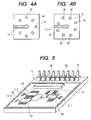
- Figs. 3A, 3B, and 3C are diagrams for explaining the configuration of another example of the millimeter wave transmission line 16 extended vertically to the layers.
- Figs. 3A and 3B are a perspective view and a cross section, respectively, of the vertical transmission line 16.
- Fig. 3B is a plan view of one layer.
- the metallic pattern 17-1 made by the surface metallic layer is formed and connected to the MMIC (not shown).
- the functions of the uppermost layer 17, metallic pattern 9 of the grounding metallic layer, and metallic patterns 10 and 11 in which the DC/IF signal line is formed are the same as those of the parts designated by the same reference numerals in Figs. 2A and 2B.
- Reference numeral 20 denotes a group of vias connecting the grounding metallic layers 9 and 11.
- the via group 20 is disposed so that the interval of neighboring vias is equal to the cycle which is equal to or smaller than 1/4 of the wavelength ⁇ of a transmission signal.
- the via group 20 functions as an electromagnetic wave wall to confine the electromagnetic wave propagating in parallel between the metallic layers 9 and 10 and between the metallic layers 10 and 11. Therefore, a low transmission loss which is almost equal to that in the vertical transmission line shown in Figs. 2A and 2B is achieved.
- the vias of the via group 20 are distributed in a square shape has been described in the example of Figs. 3A, 3B, and 3C, the vias can be distributed in a polygon shape having four or more sides such as a quadrangle or in a circular shape as shown in Figs. 4A and 4B.
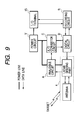
- Fig. 5 is a perspective view of the RF circuit module of Fig. 1 with the hermetic cap 4 taken away.
- RF circuit parts such as an MMIC 21 of an oscillator, an MMIC 22 of a power amplifier, MMICs 23 and 24 of a receiver, input/output connector 15, a sealing pattern 25 for airtight sealing, millimeter wave vertical transmission lines 3-1, 3-2, and 3-3, a mono layer capacitor 27, and a chip part 26 are mounted.
- the RF circuit parts construct a transmission/reception circuit of a millimeter wave radar shown in Fig. 6.
- the millimeter wave vertical transmission lines 3-1, 3-2, and 3-3 are constructed by the coaxial line 19 in Fig. 2 or the via group 20 in Fig. 3 and connected to the antenna (not shown) on the rear face.
- Fig. 6 is a block diagram showing the configuration of the transmission/reception circuit of the millimeter wave radar.
- the blocks are designated by the same numbers as those of the MMICs in Fig. 5.
- Reference numeral 22 denotes the MMIC for the power amplifier
- 23 and 24 denote the MMICs for receiver
- 3-1, 3-2, and 3-3 are the millimeter wave vertical transmission lines.
- a millimeter wave signal generated by the oscillator 21 is distributed to the power amplifier 22 and receivers 23 and 24.
- the signal amplified by the power amplifier 22 is output to the millimeter wave vertical transmission line 3-1 so as to be transmitted to the transmission antenna.
- the millimeter wave reception signal subjected to Doppler shift by the vertical transmission lines 3-2 and 3-3 are applied to the receivers 23 and 24.
- the received millimeter wave signal and a signal as a local signal from the oscillator 21 are mixed with each other to obtain an intermediate frequency signal.
- the MMICs 21 to 24 are mounted by bare chip bonding, flip chip bonding, or reflow with a liver. Since the multilayer dielectric substrate 2 is one-sided substrate, a connector, a mono layer capacitor, and a chip part can be mounted by an automatic mounter and subjected to a reflow process in a lump. To carry out the operations, it is important that the multilayer dielectric substrate 2 has a flat face irrespective of the small outer shape. In the case of die-bonding the MMIC, although it is after forming bonding wires, the RF circuit parts can operate in the state of Fig. 5. Consequently, a function test can be easily carried out. If there is a failure part, it can be easily replaced by performing reflow again.
- the sealing pattern 25 is metal plated so as to be easily bonded to the hermetic cap 4 by eutectic solder, silver paste, or the like.
- the metallic pattern 17-1 on the top face of the dielectric substrate 2-1, the metallic layer 10 for a DC/IF signal as an internal layer, the grounding metallic layers 9 and 11 to shield the DC/IF signal on and under the layer 10, and the metallic pattern 1 for the antenna on the rear face can be formed at once, so that the cost of parts and assembling cost of RF circuit module can be reduced.
- resistance to a mechanical stress moment can be improved.
- the dielectric of one layer in the multilayer substrate 2 is unignorably thick as compared with the wavelength
- a high frequency signal is transmitted vertically in the multilayer substrate, due to different potentials of the metallic layers in the multilayer substrate, each time the signal passes through the metallic layers, an electromagnetic wave which propagates parallel to the face of the metallic layer is generated.
- the electromagnetic wave wall 18 having the coaxial structure or the periodical structure which suppresses the electromagnetic wave in the transverse direction can be formed.
- the intermediate frequency signal and the power to be supplied to each of the MMICs are supplied from the outside via the input/output terminal pattern. All of the low frequency signals are transferred via the metallic layer 10 shielded by the grounding metallic layers 9 and 11 and are spatially shielded from the RF circuit parts. Thus, the millimeter wave signal transferred via the metallic layer 10 are not mixed as crosstalk.
- the transmission lines are not crossed each other, so that bonding wires for performing cubic line arrangement can be reduced.
- the millimeter wave transmission line can be linearly formed without being unnecessarily routed, and the area occupied by the RF circuits can be reduced. Consequently, reduction in the cost by designing the whole size of the multilayer dielectric substrate to be smaller and increase in the substrate life because of improvement in resistance to destruction by the mechanical stress moment are achieved.
- Fig. 7 is a sectional side view of another example of an automotive radar module according to the invention.
- the configurations of the millimeter wave circuit part 5, hard multilayer substrate 2, hermetic cap 4, and millimeter wave transmission line 6 are substantially the same as those of the example of the RF circuit module.
- a support plate 3 for assuring the mechanical strength of the antenna is disposed in the peripheral portion of the RF circuit module. Further, in order to efficiently dissipate the heat of the millimeter wave MMIC 5 to the hard multilayer substrate 2, a thermal via 7is formed so that the heat is dissipated to the antenna 1 and the support plate 3.
- a double-sided two-layer substrate having permittivity of 5 or less made of teflon or the like is used to suppress a radiation loss of the millimeter wave transmission line.
- the length of one of the sides of the hard multilayer dielectric substrate 2 is 5 cm or less, and the thickness of the substrate 2 is 0.5 mm or more so as to be resistant to a mechanical stress such as torsion or warp.
- the thickness of the dielectric of one layer in the multilayer substrate is 150 ⁇ m or less and a ceramic material such as glass ceramic or alumina ceramic is used.
- the millimeter wave MMIC 5 is mounted on the surface of the hard multilayer dielectric substrate 2, and the antenna 1 is adhered to the rear face of the hard multilayer dielectric substrate 2 so as to transmit/receive the millimeter wave signal to/from the antenna 1 via the millimeter wave transmission line 16 using the via.
- the support plate 3 is attached to the antenna 1, thereby producing effects of reinforcement of the mechanical strength of the antenna 1 and the function of a heat dissipator for dissipating heat in the hard multilayer dielectric substrate.
- a metal plate is used.
- holes of a honey comb structure are opened to enlarge the surface area and the weight of the support plate 3 can be also reduced.
- a press member obtained by pressing a steel plate having both the honey comb structure and an H-letter cross section and having a thickness of 1 mm or less can be also used.
- an electronic circuit can be mounted on the support plate 3 and a circuit for processing an IF signal obtained from the hard multilayer dielectric substrate and a power circuit can be formed.
- the automotive radar module of the embodiment has a structure such that the RF circuit module 2 is positioned to the antenna 1 and mounted and, after that, the support plate 3 is adhered so as to surround the RF circuit module.
- the mechanical strength of the RF circuit module is improved.
- the support plate 3 By adding the support plate 3, the mechanical strength of the antenna 1 is maintained.
- the millimeter wave high frequency signal transmission line is disposed on the surface and the power providing line and the low frequency signal transmission line are disposed in the intermediate layers of the grounding layers, thereby reducing crosstalk of the millimeter wave signal and realizing the multilayer wiring. Consequently, the flexibility of the wiring layout design increases, the occupied area can be reduced, and a smaller and cheaper RF circuit module can be fabricated.
- the millimeter wave signal of the millimeter wave radar is transmitted via the transmission line using a through via having the periodical structure or a through via having the coaxial structure to the rear face of the RF circuit module 2, and the power providing line and the low frequency signal transmission line are routed again to the surface of the RF circuit module 2 via the intermediate layers of the grounding layers.
- the cap 4 used for achieving the hermetic structure does not cross the signal lines, and the sealing can be safely achieved.
- Fig. 8 is a sectional side view of another example of the automotive radar module according to the invention.
- parts of a signal processing circuit (baseband signal processing circuit) other than the RF circuit module are additionally mounted on the top face (on the side opposite to the antenna conductive pattern 1) of the support plate 3 of the example shown in Fig. 7.
- the configuration of the baseband signal processing circuit is a conventionally known one. As shown in Fig.
- the module includes: an analog circuit A for processing an IF signal from an RF circuit module 4, an A/D converting circuit C for converting an output of the analog circuit A into a digital signal, a digital circuit D for processing an output of the A/D converting circuit C and supplying a control signal to the RF circuit, a recording circuit R for transmitting/receiving data to/from the digital circuit D, an input/output terminal 15 for controlling the recording circuit R, a circuit 15' as a data generating unit interposed between the input/output terminal 15 and the recording circuit R, for generating data according to a request of another electronic device on the basis of information of the recording circuit R, and a power circuit V for supplying power to the parts.
- the same parts corresponding to the circuit parts of Fig. 9 are designated by the same reference numerals. Although lines connecting the parts are formed on the top face of the support plate 3, they are not shown for simplicity of the drawing.
Landscapes
- Engineering & Computer Science (AREA)
- Electromagnetism (AREA)
- Computer Security & Cryptography (AREA)
- Radar, Positioning & Navigation (AREA)
- Remote Sensing (AREA)
- Physics & Mathematics (AREA)
- Manufacturing & Machinery (AREA)
- Microelectronics & Electronic Packaging (AREA)
- Radar Systems Or Details Thereof (AREA)
- Production Of Multi-Layered Print Wiring Board (AREA)
- Waveguides (AREA)
- Waveguide Connection Structure (AREA)
- Transceivers (AREA)
- Variable-Direction Aerials And Aerial Arrays (AREA)
- Shielding Devices Or Components To Electric Or Magnetic Fields (AREA)
Applications Claiming Priority (2)
| Application Number | Priority Date | Filing Date | Title |
|---|---|---|---|
| JP2001327225 | 2001-10-25 | ||
| JP2001327225A JP3973402B2 (ja) | 2001-10-25 | 2001-10-25 | 高周波回路モジュール |
Publications (3)
| Publication Number | Publication Date |
|---|---|
| EP1307078A2 true EP1307078A2 (de) | 2003-05-02 |
| EP1307078A3 EP1307078A3 (de) | 2004-01-28 |
| EP1307078B1 EP1307078B1 (de) | 2007-02-14 |
Family
ID=19143488
Family Applications (1)
| Application Number | Title | Priority Date | Filing Date |
|---|---|---|---|
| EP02003265A Expired - Lifetime EP1307078B1 (de) | 2001-10-25 | 2002-02-21 | Hochfrequenzschaltungsmodul |
Country Status (4)
| Country | Link |
|---|---|
| US (2) | US6794961B2 (de) |
| EP (1) | EP1307078B1 (de) |
| JP (1) | JP3973402B2 (de) |
| DE (1) | DE60218101T2 (de) |
Cited By (19)
| Publication number | Priority date | Publication date | Assignee | Title |
|---|---|---|---|---|
| GB2398430A (en) * | 2003-02-13 | 2004-08-18 | Bosch Gmbh Robert | High frequency multilayer pcb with wave guiding channel |
| EP1515389A1 (de) * | 2003-09-10 | 2005-03-16 | TDK Corporation | Mehrschichtige Hochfrequenzvorrichtung mit Planarantenne und Herstellungsverfahren |
| WO2005109330A1 (en) * | 2004-05-06 | 2005-11-17 | Fractus, S.A. | Radio-frequency system in package including antenna |
| DE102004036890A1 (de) * | 2004-07-19 | 2006-02-16 | Würth Elektronik Rot am See GmbH & Co. KG | Leiterplattenanordnung |
| EP1655803A1 (de) * | 2004-11-05 | 2006-05-10 | Hitachi, Ltd. | Hochfrequenzantenneanordnung und Verfahren für deren Herstellung |
| EP1777551A3 (de) * | 2005-10-18 | 2007-05-02 | Hitachi, Ltd. | Millimeter-Radarwellenvorrichtung und Millimeter-Radarsystem |
| EP1713310A3 (de) * | 2005-04-12 | 2008-11-26 | Pace Plc | Leiterplattenanordnung und diese enthaltendes elektrisches Gerät |
| US7463199B2 (en) | 2002-11-07 | 2008-12-09 | Fractus, S.A. | Integrated circuit package including miniature antenna |
| WO2009142983A1 (en) * | 2008-05-23 | 2009-11-26 | Alliant Techsystems Inc. | Broadband patch antenna and antenna system |
| EP2146557A1 (de) | 2008-07-15 | 2010-01-20 | Thales Holdings UK Plc | Integrierte Mikrowellenschaltung |
| EP2211423A3 (de) * | 2009-01-26 | 2010-08-04 | The Furukawa Electric Co., Ltd. | Radarantenne |
| US7924226B2 (en) | 2004-09-27 | 2011-04-12 | Fractus, S.A. | Tunable antenna |
| US8436248B2 (en) | 2005-08-05 | 2013-05-07 | Epcos Ag | Electrical component |
| EP2989483A1 (de) * | 2013-04-24 | 2016-03-02 | Hella KGaA Hueck & Co | Radareinrichtung, insbesondere für ein kraftfahrzeug |
| EP3043382A1 (de) * | 2015-01-07 | 2016-07-13 | Delphi Technologies, Inc. | Leiterplattenanordnung mit hoch- und niederfrequenten substraten |
| GB2537218A (en) * | 2015-02-24 | 2016-10-12 | Flight Refueling Ltd | Hybrid electronic circuit |
| DE102015113986A1 (de) * | 2015-08-24 | 2017-03-02 | Valeo Schalter Und Sensoren Gmbh | Sensorvorrichtung für ein Kraftfahrzeug sowie Kraftfahrzeug |
| US9972919B2 (en) | 2013-09-23 | 2018-05-15 | Samsung Electronics Co., Ltd. | Antenna apparatus and electronic device having same |
| IT201700086529A1 (it) * | 2017-07-27 | 2019-01-27 | Thales Alenia Space Italia Spa Con Unico Socio | Modulo d'antenna a microonde per applicazioni spaziali comprendente un modulo trasmetti/ricevi ibrido di tipo package su package |
Families Citing this family (126)
| Publication number | Priority date | Publication date | Assignee | Title |
|---|---|---|---|---|
| US7321485B2 (en) | 1997-04-08 | 2008-01-22 | X2Y Attenuators, Llc | Arrangement for energy conditioning |
| US7336468B2 (en) | 1997-04-08 | 2008-02-26 | X2Y Attenuators, Llc | Arrangement for energy conditioning |
| US9054094B2 (en) | 1997-04-08 | 2015-06-09 | X2Y Attenuators, Llc | Energy conditioning circuit arrangement for integrated circuit |
| US6873529B2 (en) * | 2002-02-26 | 2005-03-29 | Kyocera Corporation | High frequency module |
| FR2840112A1 (fr) * | 2002-05-23 | 2003-11-28 | Cit Alcatel | Equipement electronique hyperfrequence comportant un boitier metallique pour l'attenuation des resonances parasites |
| JP3988568B2 (ja) * | 2002-07-31 | 2007-10-10 | 松下電器産業株式会社 | 高周波モジュールおよびそれを用いた無線装置 |
| US7071545B1 (en) * | 2002-12-20 | 2006-07-04 | Asat Ltd. | Shielded integrated circuit package |
| JP2004241680A (ja) * | 2003-02-07 | 2004-08-26 | Mitsubishi Electric Corp | 多層プリント基板 |
| US7444734B2 (en) | 2003-12-09 | 2008-11-04 | International Business Machines Corporation | Apparatus and methods for constructing antennas using vias as radiating elements formed in a substrate |
| JP4634837B2 (ja) * | 2004-03-26 | 2011-02-16 | 三菱電機株式会社 | 高周波パッケージ、送受信モジュールおよび無線装置 |
| JP4634836B2 (ja) * | 2004-03-26 | 2011-02-16 | 三菱電機株式会社 | 高周波パッケージ、送受信モジュールおよび無線装置 |
| US7336221B2 (en) | 2004-03-26 | 2008-02-26 | Mitsubishi Denki Kabushiki Kaisha | High frequency package, transmitting and receiving module and wireless equipment |
| JP4553627B2 (ja) * | 2004-04-30 | 2010-09-29 | 太陽誘電株式会社 | 高周波回路モジュールおよび無線通信機器 |
| US7142073B2 (en) * | 2004-06-29 | 2006-11-28 | Intel Corporation | Transmission line impedance matching |
| US7705695B2 (en) | 2004-07-23 | 2010-04-27 | Nec Corporation | Composite via structures and filters in multilayer printed circuit boards |
| US7630188B2 (en) | 2005-03-01 | 2009-12-08 | X2Y Attenuators, Llc | Conditioner with coplanar conductors |
| JP2006246234A (ja) * | 2005-03-04 | 2006-09-14 | Hitachi Metals Ltd | 高周波スイッチモジュールおよびこれを用いた無線通信装置 |
| JP4575247B2 (ja) * | 2005-07-11 | 2010-11-04 | 株式会社東芝 | 高周波パッケージ装置 |
| JP4810904B2 (ja) | 2005-07-20 | 2011-11-09 | ソニー株式会社 | 高周波スイッチ回路を有する高周波装置 |
| JP4889974B2 (ja) * | 2005-08-01 | 2012-03-07 | 新光電気工業株式会社 | 電子部品実装構造体及びその製造方法 |
| JP4620576B2 (ja) * | 2005-12-02 | 2011-01-26 | パナソニック株式会社 | 無線装置 |
| US7463113B2 (en) * | 2006-02-28 | 2008-12-09 | Motorla, Inc. | Apparatus and methods relating to electrically conductive path interfaces disposed within capacitor plate openings |
| US7880283B2 (en) * | 2006-04-25 | 2011-02-01 | International Rectifier Corporation | High reliability power module |
| KR100712419B1 (ko) * | 2006-06-08 | 2007-04-27 | 전자부품연구원 | 대역통과필터 |
| US8736397B2 (en) * | 2006-09-07 | 2014-05-27 | Omnitracs, Llc | Ku-band coaxial to microstrip mixed dielectric PCB interface with surface mount diplexer |
| JP5194440B2 (ja) | 2006-11-24 | 2013-05-08 | 日本電気株式会社 | プリント配線基板 |
| KR100981520B1 (ko) * | 2006-12-21 | 2010-09-10 | 삼성전자주식회사 | 통신 시스템에서 전력 증폭기 장치 |
| US7477197B2 (en) * | 2006-12-29 | 2009-01-13 | Intel Corporation | Package level integration of antenna and RF front-end module |
| KR101335987B1 (ko) | 2007-01-11 | 2013-12-04 | 삼성전자주식회사 | 다층 인쇄회로기판 |
| US20080251275A1 (en) * | 2007-04-12 | 2008-10-16 | Ralph Morrison | Decoupling Transmission Line |
| KR100851076B1 (ko) | 2007-04-30 | 2008-08-12 | 삼성전기주식회사 | 전자기 밴드갭 구조물 및 인쇄회로기판 |
| KR100851075B1 (ko) * | 2007-04-30 | 2008-08-12 | 삼성전기주식회사 | 전자기 밴드갭 구조물 및 인쇄회로기판 |
| KR100851065B1 (ko) * | 2007-04-30 | 2008-08-12 | 삼성전기주식회사 | 전자기 밴드갭 구조물 및 인쇄회로기판 |
| US20080290959A1 (en) * | 2007-05-22 | 2008-11-27 | Mohammed Ershad Ali | Millimeter wave integrated circuit interconnection scheme |
| KR100850759B1 (ko) * | 2007-06-11 | 2008-08-06 | 삼성전기주식회사 | 인쇄회로기판 및 그 제조방법 |
| KR100838244B1 (ko) * | 2007-06-22 | 2008-06-17 | 삼성전기주식회사 | 전자기 밴드갭 구조물 및 인쇄회로기판 |
| KR100838246B1 (ko) * | 2007-06-22 | 2008-06-17 | 삼성전기주식회사 | 전자기 밴드갭 구조물이 구비된 인쇄회로기판 |
| KR100871347B1 (ko) * | 2007-06-22 | 2008-12-01 | 삼성전기주식회사 | 전자기 밴드갭 구조물 및 인쇄회로기판 |
| KR100871346B1 (ko) * | 2007-06-22 | 2008-12-01 | 삼성전기주식회사 | 전자기 밴드갭 구조물 및 인쇄회로기판 |
| JP2009017112A (ja) * | 2007-07-03 | 2009-01-22 | Sharp Corp | 遮蔽構造、遮蔽構造を備える衛星放送受信用コンバータ、および遮蔽構造を備える衛星放送受信用アンテナ装置 |
| KR100848848B1 (ko) * | 2007-07-12 | 2008-07-28 | 삼성전기주식회사 | 전자기 밴드갭 구조물, 이를 포함하는 인쇄회로기판과 그제조방법 |
| US8514036B2 (en) * | 2007-08-14 | 2013-08-20 | Wemtec, Inc. | Apparatus and method for mode suppression in microwave and millimeterwave packages |
| US8816798B2 (en) * | 2007-08-14 | 2014-08-26 | Wemtec, Inc. | Apparatus and method for electromagnetic mode suppression in microwave and millimeterwave packages |
| US9000869B2 (en) | 2007-08-14 | 2015-04-07 | Wemtec, Inc. | Apparatus and method for broadband electromagnetic mode suppression in microwave and millimeterwave packages |
| KR100913363B1 (ko) | 2007-09-18 | 2009-08-20 | 삼성전기주식회사 | 멀티 비아를 포함하는 전자기 밴드갭 구조물 및인쇄회로기판 |
| JP4998274B2 (ja) * | 2008-01-10 | 2012-08-15 | セイコーエプソン株式会社 | セラミック多層基板の製造方法 |
| JP5294828B2 (ja) * | 2008-01-28 | 2013-09-18 | 京セラ株式会社 | 積層基板 |
| US7830301B2 (en) | 2008-04-04 | 2010-11-09 | Toyota Motor Engineering & Manufacturing North America, Inc. | Dual-band antenna array and RF front-end for automotive radars |
| US7733265B2 (en) * | 2008-04-04 | 2010-06-08 | Toyota Motor Engineering & Manufacturing North America, Inc. | Three dimensional integrated automotive radars and methods of manufacturing the same |
| US8022861B2 (en) | 2008-04-04 | 2011-09-20 | Toyota Motor Engineering & Manufacturing North America, Inc. | Dual-band antenna array and RF front-end for mm-wave imager and radar |
| JP2010098274A (ja) * | 2008-10-20 | 2010-04-30 | Sibeam Inc | 表面実装可能な集積回路のパッケージ化機構 |
| US7990237B2 (en) * | 2009-01-16 | 2011-08-02 | Toyota Motor Engineering & Manufacturing North America, Inc. | System and method for improving performance of coplanar waveguide bends at mm-wave frequencies |
| KR101009080B1 (ko) | 2009-02-02 | 2011-01-18 | 삼성전기주식회사 | 방열 인쇄회로기판 및 그 제조방법 |
| CN101997168B (zh) * | 2009-08-26 | 2013-08-21 | 智易科技股份有限公司 | 双频双天线结构 |
| US8536954B2 (en) * | 2010-06-02 | 2013-09-17 | Siklu Communication ltd. | Millimeter wave multi-layer packaging including an RFIC cavity and a radiating cavity therein |
| EP2504887B1 (de) * | 2009-11-27 | 2020-01-08 | BAE Systems PLC | Antennenanordnung |
| US8558637B2 (en) * | 2010-05-12 | 2013-10-15 | Mediatek Inc. | Circuit device with signal line transition element |
| US8786496B2 (en) | 2010-07-28 | 2014-07-22 | Toyota Motor Engineering & Manufacturing North America, Inc. | Three-dimensional array antenna on a substrate with enhanced backlobe suppression for mm-wave automotive applications |
| US8975978B2 (en) * | 2010-08-30 | 2015-03-10 | Nec Corporation | Interconnect substrate and electronic device |
| KR101179399B1 (ko) | 2010-10-04 | 2012-09-04 | 삼성전기주식회사 | 크로스토크를 저감하기 위한 인쇄회로기판 |
| KR20120035394A (ko) * | 2010-10-05 | 2012-04-16 | 삼성전자주식회사 | 수직구조의 전송선로 트랜지션 및 랜드 그리드 어레이 접합를 이용한 단일 칩 패키지를 위한 장치 |
| US9386688B2 (en) | 2010-11-12 | 2016-07-05 | Freescale Semiconductor, Inc. | Integrated antenna package |
| US9553371B2 (en) | 2010-11-12 | 2017-01-24 | Nxp Usa, Inc. | Radar module |
| DE102011005145A1 (de) | 2011-03-04 | 2012-09-06 | Rohde & Schwarz Gmbh & Co. Kg | Leiterplattenanordnung für Millimeterwellen-Scanner |
| JP2013118354A (ja) * | 2011-11-02 | 2013-06-13 | Japan Electronic Materials Corp | 多層絶縁基板および多層絶縁基板の製造方法 |
| KR101426584B1 (ko) * | 2011-12-09 | 2014-08-06 | 주식회사 만도 | 레이더 장치 및 그 조립 방법 |
| KR101450316B1 (ko) | 2012-01-17 | 2014-10-21 | 주식회사 만도 | 레이더 장치 및 그 조립 방법 |
| US8653467B2 (en) * | 2012-06-19 | 2014-02-18 | Raytheon Company | Multichip packaging for imaging system |
| CN104604345A (zh) * | 2012-08-31 | 2015-05-06 | 索尼公司 | 布线板及布线板的制造方法 |
| US8791550B1 (en) | 2013-01-15 | 2014-07-29 | International Business Machines Corporation | Hybrid conductor through-silicon-via for power distribution and signal transmission |
| JP5762452B2 (ja) * | 2013-02-05 | 2015-08-12 | サイビーム インコーポレイテッド | 表面実装可能な集積回路のパッケージ化機構 |
| US10103447B2 (en) | 2014-06-13 | 2018-10-16 | Nxp Usa, Inc. | Integrated circuit package with radio frequency coupling structure |
| US9917372B2 (en) | 2014-06-13 | 2018-03-13 | Nxp Usa, Inc. | Integrated circuit package with radio frequency coupling arrangement |
| US9887449B2 (en) * | 2014-08-29 | 2018-02-06 | Nxp Usa, Inc. | Radio frequency coupling structure and a method of manufacturing thereof |
| US10225925B2 (en) * | 2014-08-29 | 2019-03-05 | Nxp Usa, Inc. | Radio frequency coupling and transition structure |
| EP3016204A1 (de) * | 2014-11-03 | 2016-05-04 | Thomson Licensing | Antennenanordnung und elektronische Vorrichtung mit dieser Antennenanordnung |
| JP6348396B2 (ja) * | 2014-10-07 | 2018-06-27 | 株式会社Soken | アンテナ装置 |
| JP6894602B2 (ja) * | 2014-11-28 | 2021-06-30 | 国立大学法人 岡山大学 | 印刷配線板およびその製造方法 |
| US10178758B2 (en) | 2014-11-28 | 2019-01-08 | National University Corporation Okayama University | Printed wiring board and method of producing the same |
| JP6515558B2 (ja) * | 2015-02-04 | 2019-05-22 | 富士通株式会社 | 積層型導波路、無線通信モジュール、及び、無線通信システム |
| TWI551484B (zh) * | 2015-06-17 | 2016-10-01 | 啟碁科技股份有限公司 | 電子裝置及雷達裝置 |
| JP6494458B2 (ja) * | 2015-07-16 | 2019-04-03 | 三菱電機株式会社 | 同軸線路形回路、同軸線路形回路の組立方法、および同軸線路形回路を用いたアレイアンテナ装置 |
| JP6672639B2 (ja) * | 2015-08-26 | 2020-03-25 | カシオ計算機株式会社 | 誘電体アンテナ |
| CN105578714A (zh) * | 2015-12-11 | 2016-05-11 | 广东顺德中山大学卡内基梅隆大学国际联合研究院 | 一种多层高速pcb的新型叠层结构及信号过孔优化方法 |
| DE112015007234T5 (de) * | 2015-12-26 | 2018-10-04 | Intel Corporation | Vertikale masseebenenisolierung, masseleiter-koaxialisolierung und impedanzabstimmung von durch gehäusevorrichtungen geführten horizontalen datensignalübertragungsleitungen |
| JP2018018935A (ja) * | 2016-07-27 | 2018-02-01 | イビデン株式会社 | プリント配線板及びその製造方法 |
| KR20180054079A (ko) * | 2016-11-15 | 2018-05-24 | 인지니어스 주식회사 | 차폐기판을 포함하는 레이더 모듈 |
| JP2018088629A (ja) * | 2016-11-29 | 2018-06-07 | ソニーセミコンダクタソリューションズ株式会社 | 高周波モジュール、および通信装置 |
| US20180184550A1 (en) | 2016-12-28 | 2018-06-28 | Microsoft Technology Licensing, Llc | Metal additive structures on printed circuit boards |
| US10396432B2 (en) * | 2017-01-23 | 2019-08-27 | Samsung Electro-Mechanics Co., Ltd. | Antenna-integrated radio frequency module |
| US10178764B2 (en) * | 2017-06-05 | 2019-01-08 | Waymo Llc | PCB optical isolation by nonuniform catch pad stack |
| US10714430B2 (en) * | 2017-07-21 | 2020-07-14 | Octavo Systems Llc | EMI shield for molded packages |
| US10901068B2 (en) * | 2017-08-14 | 2021-01-26 | Smartcover Systems | Manhole cover roadway radar safety device |
| JP6905438B2 (ja) | 2017-09-22 | 2021-07-21 | 株式会社フジクラ | 無線通信モジュール |
| US11160163B2 (en) * | 2017-11-17 | 2021-10-26 | Texas Instruments Incorporated | Electronic substrate having differential coaxial vias |
| DE102018202544A1 (de) | 2018-02-20 | 2019-08-22 | Audi Ag | Systeme zum Übermitteln von Signalen |
| KR102034308B1 (ko) * | 2018-02-28 | 2019-10-18 | 삼성전자주식회사 | 안테나 모듈 |
| DE102018203106A1 (de) * | 2018-03-01 | 2019-09-05 | Conti Temic Microelectronic Gmbh | Radarsystem zur Umfelderfassung eines Kraftfahrzeugs mit einer Kunststoffantenne |
| US11799182B2 (en) | 2018-03-09 | 2023-10-24 | Furukawa Electric Co., Ltd. | High-frequency transmission line, radar apparatus provided with high-frequency transmission line, and wireless device |
| JP6777136B2 (ja) * | 2018-11-20 | 2020-10-28 | Tdk株式会社 | アンテナモジュール |
| US11289802B2 (en) * | 2019-04-08 | 2022-03-29 | Apple Inc. | Millimeter wave impedance matching structures |
| KR102578395B1 (ko) * | 2019-04-25 | 2023-09-14 | 엘지전자 주식회사 | 커넥터를 구비하는 전자 기기 |
| US11955706B2 (en) * | 2019-04-25 | 2024-04-09 | Lg Electronics Inc. | Electronic device including connector |
| US11464109B2 (en) | 2019-05-16 | 2022-10-04 | Samsung Electronics Co., Ltd. | Printed circuit board including coaxial plated through hole and electronic apparatus including same in wireless communication system |
| US11244913B2 (en) * | 2019-06-18 | 2022-02-08 | Mediatek Inc. | Semiconductor package |
| CN110289493B (zh) * | 2019-07-20 | 2024-03-29 | 深圳市全智芯科技有限公司 | 一种微波感应雷达天线的布线结构 |
| KR102076750B1 (ko) * | 2019-09-06 | 2020-02-12 | 주식회사 가가 | 레이더를 이용한 크레인 충돌 방지 센서 |
| CN110865434B (zh) * | 2019-11-21 | 2021-01-15 | 中国科学院半导体研究所 | 一体化微波电路 |
| JP7355640B2 (ja) * | 2019-12-23 | 2023-10-03 | 日立Astemo株式会社 | 電子制御装置 |
| CN111090076A (zh) * | 2020-01-22 | 2020-05-01 | 无锡威孚高科技集团股份有限公司 | 一种毫米波雷达射频前端电路结构及其制作方法 |
| JP7422360B2 (ja) * | 2020-03-02 | 2024-01-26 | 株式会社デンソー | 半導体パッケージ |
| KR20210138418A (ko) * | 2020-05-12 | 2021-11-19 | 삼성전자주식회사 | 안테나 모듈 및 상기 안테나 모듈을 포함하는 전자 장치 |
| CN111540510A (zh) * | 2020-05-26 | 2020-08-14 | 珠海市魅族科技有限公司 | 中频信号传输结构及电子设备 |
| DE102020211254A1 (de) * | 2020-09-08 | 2022-03-10 | Conti Temic Microelectronic Gmbh | Radarsystem zur Umgebungserfassung mit einer Wellenleiterantenne gebildet aus einer Platine und einem Formteil |
| CN113097183B (zh) * | 2021-03-29 | 2024-02-09 | 电子科技大学 | 一种基于硅通孔的射频垂直互连传输结构 |
| KR102904490B1 (ko) | 2021-05-25 | 2025-12-29 | 삼성전자 주식회사 | 안테나 모듈 및 이를 포함하는 전자 장치 |
| US20220416391A1 (en) * | 2021-06-23 | 2022-12-29 | Intel Corporation | Signal and ground vias in a glass core to control impedance |
| US12069805B2 (en) * | 2021-09-13 | 2024-08-20 | Apple Inc. | Wideband millimeter wave via transition |
| CN114096138A (zh) * | 2021-11-17 | 2022-02-25 | 吉林大学 | 一种基于电磁干扰屏蔽的发动机ecu防护方法 |
| CN114126204B (zh) * | 2021-11-19 | 2023-07-25 | 中国电子科技集团公司第二十九研究所 | 一种基于金属基复合基板的微波数字混合组件 |
| CN113948848B (zh) * | 2021-12-20 | 2022-04-12 | 成都瑞迪威科技有限公司 | 一种接地良好的天线互联结构 |
| CN114743946B (zh) * | 2022-03-14 | 2026-01-09 | 加特兰微电子科技(上海)有限公司 | 一种集成毫米波雷达天线的芯片封装结构及其封装方法 |
| CN114900947B (zh) * | 2022-04-15 | 2025-04-25 | 深南电路股份有限公司 | 印制电路板 |
| CN115494456B (zh) * | 2022-11-21 | 2023-03-10 | 南京隼眼电子科技有限公司 | 雷达收发装置及雷达装置 |
| CN115734464B (zh) * | 2023-01-06 | 2023-05-05 | 四川斯艾普电子科技有限公司 | 一种厚薄膜电路基板tr组件及其封装方法 |
| WO2025099817A1 (ja) * | 2023-11-07 | 2025-05-15 | 日本電信電話株式会社 | 半導体装置 |
Family Cites Families (15)
| Publication number | Priority date | Publication date | Assignee | Title |
|---|---|---|---|---|
| JPS61239701A (ja) | 1985-04-16 | 1986-10-25 | Mitsubishi Electric Corp | トリプレ−ト線路形t分岐 |
| JPH04802A (ja) | 1990-04-17 | 1992-01-06 | Mitsubishi Electric Corp | トリプレート線路形基板間接続素子 |
| JP2840493B2 (ja) | 1991-12-27 | 1998-12-24 | 株式会社日立製作所 | 一体型マイクロ波回路 |
| FR2710195B1 (fr) | 1993-09-14 | 1995-10-13 | Thomson Csf | Assemblage antenne-circuit électronique. |
| US5521406A (en) * | 1994-08-31 | 1996-05-28 | Texas Instruments Incorporated | Integrated circuit with improved thermal impedance |
| EP0764393B1 (de) * | 1995-03-02 | 2001-07-04 | Circuit Components, Incorporated | Kostengünstiges hochleistungsgehäuse für mikrowellenschaltungen im 90 ghz-bereich mit bga ein/ausgangsformat und keramischer substrattechnologie |
| JPH08250913A (ja) | 1995-03-15 | 1996-09-27 | Honda Motor Co Ltd | Mmicパッケージ組立 |
| JP3266491B2 (ja) | 1996-02-29 | 2002-03-18 | 京セラ株式会社 | 高周波用パッケージ |
| JPH11251829A (ja) * | 1998-02-27 | 1999-09-17 | Kyocera Corp | スロットアンテナ及びそれを具備する配線基板 |
| US6215377B1 (en) | 1998-05-26 | 2001-04-10 | Microsubstrates Corporation | Low cost wideband RF port structure for microwave circuit packages using coplanar waveguide and BGA I/O format |
| EP0978729A3 (de) * | 1998-08-07 | 2002-03-20 | Hitachi, Ltd. | Hochfrequenz-Sende-Empfangsvorrichtung für Fahrzeug-Radarsysteme |
| US6154176A (en) * | 1998-08-07 | 2000-11-28 | Sarnoff Corporation | Antennas formed using multilayer ceramic substrates |
| JP2001185918A (ja) | 1999-12-24 | 2001-07-06 | Kyocera Corp | 高周波用配線基板 |
| US6828556B2 (en) * | 2001-09-28 | 2004-12-07 | Hrl Laboratories, Llc | Millimeter wave imaging array |
| JP2005086603A (ja) * | 2003-09-10 | 2005-03-31 | Tdk Corp | 電子部品モジュールおよびその製造方法 |
-
2001
- 2001-10-25 JP JP2001327225A patent/JP3973402B2/ja not_active Expired - Fee Related
-
2002
- 2002-02-08 US US10/067,917 patent/US6794961B2/en not_active Expired - Fee Related
- 2002-02-21 EP EP02003265A patent/EP1307078B1/de not_active Expired - Lifetime
- 2002-02-21 DE DE60218101T patent/DE60218101T2/de not_active Expired - Lifetime
-
2004
- 2004-09-01 US US10/931,115 patent/US7239222B2/en not_active Expired - Fee Related
Cited By (34)
| Publication number | Priority date | Publication date | Assignee | Title |
|---|---|---|---|---|
| US7463199B2 (en) | 2002-11-07 | 2008-12-09 | Fractus, S.A. | Integrated circuit package including miniature antenna |
| US9077073B2 (en) | 2002-11-07 | 2015-07-07 | Fractus, S.A. | Integrated circuit package including miniature antenna |
| US8203488B2 (en) | 2002-11-07 | 2012-06-19 | Fractus, S.A. | Integrated circuit package including miniature antenna |
| US7791539B2 (en) | 2002-11-07 | 2010-09-07 | Fractus, S.A. | Radio-frequency system in package including antenna |
| US9761948B2 (en) | 2002-11-07 | 2017-09-12 | Fractus, S.A. | Integrated circuit package including miniature antenna |
| US10644405B2 (en) | 2002-11-07 | 2020-05-05 | Fractus, S.A. | Integrated circuit package including miniature antenna |
| US10056691B2 (en) | 2002-11-07 | 2018-08-21 | Fractus, S.A. | Integrated circuit package including miniature antenna |
| US10320079B2 (en) | 2002-11-07 | 2019-06-11 | Fractus, S.A. | Integrated circuit package including miniature antenna |
| US8421686B2 (en) | 2002-11-07 | 2013-04-16 | Fractus, S.A. | Radio-frequency system in package including antenna |
| GB2398430A (en) * | 2003-02-13 | 2004-08-18 | Bosch Gmbh Robert | High frequency multilayer pcb with wave guiding channel |
| US7236070B2 (en) | 2003-09-10 | 2007-06-26 | Tdk Corporation | Electronic component module and manufacturing method thereof |
| EP1515389A1 (de) * | 2003-09-10 | 2005-03-16 | TDK Corporation | Mehrschichtige Hochfrequenzvorrichtung mit Planarantenne und Herstellungsverfahren |
| WO2005109330A1 (en) * | 2004-05-06 | 2005-11-17 | Fractus, S.A. | Radio-frequency system in package including antenna |
| DE102004036890A1 (de) * | 2004-07-19 | 2006-02-16 | Würth Elektronik Rot am See GmbH & Co. KG | Leiterplattenanordnung |
| US7924226B2 (en) | 2004-09-27 | 2011-04-12 | Fractus, S.A. | Tunable antenna |
| US7456790B2 (en) | 2004-11-05 | 2008-11-25 | Hitachi, Ltd. | High frequency antenna device and method of manufacturing the same, HF antenna printed circuit board for HF antenna device, and transmitting and receiving device using HF antenna device |
| EP1655803A1 (de) * | 2004-11-05 | 2006-05-10 | Hitachi, Ltd. | Hochfrequenzantenneanordnung und Verfahren für deren Herstellung |
| EP1713310A3 (de) * | 2005-04-12 | 2008-11-26 | Pace Plc | Leiterplattenanordnung und diese enthaltendes elektrisches Gerät |
| US8436248B2 (en) | 2005-08-05 | 2013-05-07 | Epcos Ag | Electrical component |
| EP1777551A3 (de) * | 2005-10-18 | 2007-05-02 | Hitachi, Ltd. | Millimeter-Radarwellenvorrichtung und Millimeter-Radarsystem |
| US8232924B2 (en) | 2008-05-23 | 2012-07-31 | Alliant Techsystems Inc. | Broadband patch antenna and antenna system |
| WO2009142983A1 (en) * | 2008-05-23 | 2009-11-26 | Alliant Techsystems Inc. | Broadband patch antenna and antenna system |
| EP2146557A1 (de) | 2008-07-15 | 2010-01-20 | Thales Holdings UK Plc | Integrierte Mikrowellenschaltung |
| EP2211423A3 (de) * | 2009-01-26 | 2010-08-04 | The Furukawa Electric Co., Ltd. | Radarantenne |
| EP2989483A1 (de) * | 2013-04-24 | 2016-03-02 | Hella KGaA Hueck & Co | Radareinrichtung, insbesondere für ein kraftfahrzeug |
| EP3051628B1 (de) * | 2013-09-23 | 2019-07-10 | Samsung Electronics Co., Ltd. | Antennenvorrichtung und elektronische vorrichtung damit |
| US9972919B2 (en) | 2013-09-23 | 2018-05-15 | Samsung Electronics Co., Ltd. | Antenna apparatus and electronic device having same |
| EP3043382A1 (de) * | 2015-01-07 | 2016-07-13 | Delphi Technologies, Inc. | Leiterplattenanordnung mit hoch- und niederfrequenten substraten |
| GB2537218A (en) * | 2015-02-24 | 2016-10-12 | Flight Refueling Ltd | Hybrid electronic circuit |
| GB2537218B (en) * | 2015-02-24 | 2020-01-29 | Cobham Mission Systems Wimborne Ltd | Hybrid electronic circuit |
| DE102015113986A1 (de) * | 2015-08-24 | 2017-03-02 | Valeo Schalter Und Sensoren Gmbh | Sensorvorrichtung für ein Kraftfahrzeug sowie Kraftfahrzeug |
| IT201700086529A1 (it) * | 2017-07-27 | 2019-01-27 | Thales Alenia Space Italia Spa Con Unico Socio | Modulo d'antenna a microonde per applicazioni spaziali comprendente un modulo trasmetti/ricevi ibrido di tipo package su package |
| EP3435111A1 (de) * | 2017-07-27 | 2019-01-30 | Thales Alenia Space Italia S.p.A. Con Unico Socio | Mikrowellenantennenmodul für raumanwendungen mit einem hybriden sende-/empfangsmodul des typs packet auf packet |
| US10665952B2 (en) | 2017-07-27 | 2020-05-26 | Thales Alenia Space Italia S.P.A. Con Unico Socio | Microwave antenna module for space applications including a hybrid transmit/receive module of package on package type |
Also Published As
| Publication number | Publication date |
|---|---|
| US6794961B2 (en) | 2004-09-21 |
| US20050030231A1 (en) | 2005-02-10 |
| US7239222B2 (en) | 2007-07-03 |
| DE60218101D1 (de) | 2007-03-29 |
| EP1307078A3 (de) | 2004-01-28 |
| EP1307078B1 (de) | 2007-02-14 |
| JP3973402B2 (ja) | 2007-09-12 |
| US20030080836A1 (en) | 2003-05-01 |
| DE60218101T2 (de) | 2007-08-16 |
| JP2003133801A (ja) | 2003-05-09 |
Similar Documents
| Publication | Publication Date | Title |
|---|---|---|
| US6794961B2 (en) | High frequency circuit module | |
| US6335669B1 (en) | RF circuit module | |
| EP1515389B1 (de) | Mehrschichtige Hochfrequenzvorrichtung mit Planarantenne und Herstellungsverfahren | |
| US5644277A (en) | Three-wire-line vertical interconnect structure for multilevel substrates | |
| US5019829A (en) | Plug-in package for microwave integrated circuit having cover-mounted antenna | |
| US7964937B2 (en) | Multilayer dielectric substrate and semiconductor package | |
| US7911292B2 (en) | Mode transition between a planar line and a waveguide with a low loss RF substrate and a high loss low frequency substrate | |
| US6483406B1 (en) | High-frequency module using slot coupling | |
| US8362608B2 (en) | Ultra wideband hermetically sealed surface mount technology for microwave monolithic integrated circuit package | |
| EP2428989B1 (de) | Hochfrequenzschaltungsgehäuse und Hochfrequenzschaltung | |
| KR100713195B1 (ko) | 고주파모듈 및 그 제조방법 | |
| US6489679B2 (en) | High-frequency package | |
| JP3537626B2 (ja) | 高周波用パッケージ | |
| JP2571029B2 (ja) | マイクロ波集積回路 | |
| JP2616698B2 (ja) | 複合高周波回路モジュール | |
| JP3305589B2 (ja) | 高周波用半導体装置の実装構造 | |
| JP3556470B2 (ja) | 高周波用モジュール | |
| JP2004297465A (ja) | 高周波用パッケージ | |
| JP3439967B2 (ja) | 高周波半導体素子用パッケージ | |
| JP2011010242A (ja) | 高周波基板および高周波モジュール | |
| JP2006067376A (ja) | アンテナモジュール | |
| JP2006067375A (ja) | アンテナモジュール | |
| JP3071761B2 (ja) | 高周波用半導体装置の実装構造 | |
| JPH11345910A (ja) | 高周波用配線基板の接続構造 | |
| JP2010041714A (ja) | 高周波基板および高周波モジュール |
Legal Events
| Date | Code | Title | Description |
|---|---|---|---|
| PUAI | Public reference made under article 153(3) epc to a published international application that has entered the european phase |
Free format text: ORIGINAL CODE: 0009012 |
|
| AK | Designated contracting states |
Designated state(s): AT BE CH CY DE DK ES FI FR GB GR IE IT LI LU MC NL PT SE TR |
|
| AX | Request for extension of the european patent |
Extension state: AL LT LV MK RO SI |
|
| PUAL | Search report despatched |
Free format text: ORIGINAL CODE: 0009013 |
|
| AK | Designated contracting states |
Kind code of ref document: A3 Designated state(s): AT BE CH CY DE DK ES FI FR GB GR IE IT LI LU MC NL PT SE TR |
|
| AX | Request for extension of the european patent |
Extension state: AL LT LV MK RO SI |
|
| RIC1 | Information provided on ipc code assigned before grant |
Ipc: 7H 01Q 23/00 B Ipc: 7H 01P 3/08 B Ipc: 7H 01Q 1/32 A Ipc: 7H 01Q 21/00 B Ipc: 7H 01P 5/02 B Ipc: 7H 01Q 9/04 B |
|
| 17P | Request for examination filed |
Effective date: 20040519 |
|
| 17Q | First examination report despatched |
Effective date: 20040702 |
|
| AKX | Designation fees paid |
Designated state(s): DE FR GB IT |
|
| GRAP | Despatch of communication of intention to grant a patent |
Free format text: ORIGINAL CODE: EPIDOSNIGR1 |
|
| GRAS | Grant fee paid |
Free format text: ORIGINAL CODE: EPIDOSNIGR3 |
|
| GRAA | (expected) grant |
Free format text: ORIGINAL CODE: 0009210 |
|
| RAP1 | Party data changed (applicant data changed or rights of an application transferred) |
Owner name: HITACHI, LTD. |
|
| AK | Designated contracting states |
Kind code of ref document: B1 Designated state(s): DE FR GB IT |
|
| REG | Reference to a national code |
Ref country code: GB Ref legal event code: FG4D |
|
| REF | Corresponds to: |
Ref document number: 60218101 Country of ref document: DE Date of ref document: 20070329 Kind code of ref document: P |
|
| ET | Fr: translation filed | ||
| PLBE | No opposition filed within time limit |
Free format text: ORIGINAL CODE: 0009261 |
|
| STAA | Information on the status of an ep patent application or granted ep patent |
Free format text: STATUS: NO OPPOSITION FILED WITHIN TIME LIMIT |
|
| 26N | No opposition filed |
Effective date: 20071115 |
|
| PGFP | Annual fee paid to national office [announced via postgrant information from national office to epo] |
Ref country code: FR Payment date: 20120221 Year of fee payment: 11 |
|
| PGFP | Annual fee paid to national office [announced via postgrant information from national office to epo] |
Ref country code: DE Payment date: 20120215 Year of fee payment: 11 |
|
| PGFP | Annual fee paid to national office [announced via postgrant information from national office to epo] |
Ref country code: GB Payment date: 20120215 Year of fee payment: 11 Ref country code: IT Payment date: 20120216 Year of fee payment: 11 |
|
| GBPC | Gb: european patent ceased through non-payment of renewal fee |
Effective date: 20130221 |
|
| REG | Reference to a national code |
Ref country code: FR Ref legal event code: ST Effective date: 20131031 |
|
| REG | Reference to a national code |
Ref country code: DE Ref legal event code: R119 Ref document number: 60218101 Country of ref document: DE Effective date: 20130903 |
|
| PG25 | Lapsed in a contracting state [announced via postgrant information from national office to epo] |
Ref country code: IT Free format text: LAPSE BECAUSE OF NON-PAYMENT OF DUE FEES Effective date: 20130221 |
|
| PG25 | Lapsed in a contracting state [announced via postgrant information from national office to epo] |
Ref country code: GB Free format text: LAPSE BECAUSE OF NON-PAYMENT OF DUE FEES Effective date: 20130221 Ref country code: FR Free format text: LAPSE BECAUSE OF NON-PAYMENT OF DUE FEES Effective date: 20130228 Ref country code: DE Free format text: LAPSE BECAUSE OF NON-PAYMENT OF DUE FEES Effective date: 20130903 |