EP1307080A2 - Module électronique et méthode pour le produire - Google Patents
Module électronique et méthode pour le produire Download PDFInfo
- Publication number
- EP1307080A2 EP1307080A2 EP02023668A EP02023668A EP1307080A2 EP 1307080 A2 EP1307080 A2 EP 1307080A2 EP 02023668 A EP02023668 A EP 02023668A EP 02023668 A EP02023668 A EP 02023668A EP 1307080 A2 EP1307080 A2 EP 1307080A2
- Authority
- EP
- European Patent Office
- Prior art keywords
- conductor tracks
- housing
- base body
- electronic components
- body housing
- Prior art date
- Legal status (The legal status is an assumption and is not a legal conclusion. Google has not performed a legal analysis and makes no representation as to the accuracy of the status listed.)
- Granted
Links
Images


Classifications
-
- H—ELECTRICITY
- H05—ELECTRIC TECHNIQUES NOT OTHERWISE PROVIDED FOR
- H05K—PRINTED CIRCUITS; CASINGS OR CONSTRUCTIONAL DETAILS OF ELECTRIC APPARATUS; MANUFACTURE OF ASSEMBLAGES OF ELECTRICAL COMPONENTS
- H05K3/00—Apparatus or processes for manufacturing printed circuits
- H05K3/10—Apparatus or processes for manufacturing printed circuits in which conductive material is applied to the insulating support in such a manner as to form the desired conductive pattern
- H05K3/18—Apparatus or processes for manufacturing printed circuits in which conductive material is applied to the insulating support in such a manner as to form the desired conductive pattern using precipitation techniques to apply the conductive material
- H05K3/181—Apparatus or processes for manufacturing printed circuits in which conductive material is applied to the insulating support in such a manner as to form the desired conductive pattern using precipitation techniques to apply the conductive material by electroless plating
- H05K3/182—Apparatus or processes for manufacturing printed circuits in which conductive material is applied to the insulating support in such a manner as to form the desired conductive pattern using precipitation techniques to apply the conductive material by electroless plating characterised by the patterning method
-
- H—ELECTRICITY
- H05—ELECTRIC TECHNIQUES NOT OTHERWISE PROVIDED FOR
- H05K—PRINTED CIRCUITS; CASINGS OR CONSTRUCTIONAL DETAILS OF ELECTRIC APPARATUS; MANUFACTURE OF ASSEMBLAGES OF ELECTRICAL COMPONENTS
- H05K1/00—Printed circuits
- H05K1/02—Details
- H05K1/0284—Details of three-dimensional rigid printed circuit boards
Definitions
- the invention relates to an electronic module and to a method of producing the electronic module, in which the electronic components are connected in a plastic housing by conductor tracks.
- the present invention provides a method of producing an electronic module by means of which conventional printed circuit boards are no longer necessary and components such as acceleration sensors can be positioned in various orientations inside the plastic housing that has been made with one and the same tool.
- a base body housing is made of an electrically non-conductive plastic with recessed conduits.
- a galvanizable plastic is then introduced into these conduits.
- the surface of the galvanizable plastic is metallized.
- the electronic components are placed onto the conductor tracks created by the metallization and connected to them.
- the conductor tracks made in this manner can completely replace a printed circuit board. At the same time, they can replace the connection lines between a conventional printed circuit board and contact pins on the plug base of the electronic module.
- the plastic housing is preferably manufactured by means of two-component injection molding technology. For different orientations of the electronic components inside the housing, correspondingly different conductor tracks are needed.
- the conduits that have to be left open for this on the inside of the housing are created by interchangeable mold cores. However, the same injection molding tool can be used for all orientations.
- the invention also provides an electronic module that can be made by means of the method according to the invention in which the electronic components are connected in a plastic housing by means of conductor tracks.
- This housing has a base body housing made of electrically non-conductive plastic, and the inner surface of its housing wall is provided with recessed conduits. A galvanizable plastic is introduced into these conduits.
- the conductor tracks are formed by a metallization applied onto the galvanizable plastic.
- the electronic components are mounted on the conductor tracks and preferably connected to them by means of soldering.
- the invention is especially advantageous for the invention to be used for electronic modules that serve to actuate restraint systems in vehicles and that, as one of the electronic components, comprise an acceleration sensor that is arranged in a precisely defined orientation inside the plastic housing.
- the electronic module which is shown in Figure 1 with the cover removed, has a plastic housing with a generally cuboidal base body housing 10 that has two shaped-on fastening lugs 12, 14 and a likewise one-piece, shaped-on plug base 16. Inside the base body housing 10 , there is a cavity 18 in which electronic components 20, 22 and 24 are arranged. These electronic components 20, 22 and 24 are mounted on conductor tracks 26, 28 and connected to them by means of soldering.
- the electronic component designated with 20 comprises an acceleration sensor that has to have a specific orientation inside the housing. In the example shown here, the electronic component 20 is placed flat onto the bottom of the base body housing 10 .
- the plug base 16 surrounds two contact pins 30, 32, which penetrate through the wall of the base body housing and which project into the inside of the base body housing 10.
- the contact pins 30, 32 are linked by conductor track sections 26a, 28a to the conductor track system to which the electronic components 20, 22 and 24 are connected.
- the described plastic housing of the electronic module is produced by means of injection molding.
- a mold core is placed into the injection molding tool.
- the mold core has protruding ribs whose shape and arrangement correspond to the required conductor tracks.
- conduits 34 ( Figure 4) are formed on the inside surface of the base body housing 10 .
- these conduits 34 are filled with a galvanizable plastic 36 .
- Galvanizable plastics are especially those that contain palladium ions.
- a metallization 38 is galvanically deposited onto the surface of the plastic 36 that fills the conduits 34.
- the metallization 38 can consist of copper, zinc, tin or gold.
- the ends of the contact pins 30, 32 projecting into the housing are surrounded by corresponding areas of the conductor track sections 26a, 28a . During the electrochemical metallization, a connection is also made to the contact pins 30, 32.
- the conductor tracks 26, 28 lie in a shared plane since they are formed in the bottom wall of the base body housing 10 .
- a special aspect of the process described is precisely the fact that three-dimensional conductor track systems can be set up.
- the mold core placed into the injection mold merely has to have corresponding ribs on its outer surfaces.
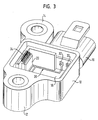
- the embodiment shown in Figures 2 and 3 differs from that of Figure 1 only through the orientation of the electronic components and the corresponding configuration and arrangement of the conductor tracks inside the base body housing.
- the electronic component 20 comprising the acceleration sensor is arranged parallel to a side surface and thus perpendicular to the bottom surface of the base body housing 10.
- This conductor track system comprises conductor tracks 26, 28 in the bottom surface of the base body housing 10 with conductor track sections 26a, 28a whose ends are bent and lead up to the contact pins 30, 32. However, it also comprises conductor tracks 34 that are arranged in a side wall that is perpendicular to the bottom wall of the base body housing 10 .
- the electronic component 20 is mounted on these conductor tracks 34 and soldered to them.
- the electronic component 22 is mounted on the conductor tracks 26 and soldered to them. Consequently, electronic components can be arranged and attached to different inside surfaces of the base body housing 10.
Landscapes
- Engineering & Computer Science (AREA)
- Manufacturing & Machinery (AREA)
- Microelectronics & Electronic Packaging (AREA)
- Injection Moulding Of Plastics Or The Like (AREA)
- Pressure Sensors (AREA)
- Casings For Electric Apparatus (AREA)
Priority Applications (1)
| Application Number | Priority Date | Filing Date | Title |
|---|---|---|---|
| DE2002023668 DE1307080T1 (de) | 2001-10-23 | 2002-10-22 | Elektronisches Modul und dessen Herstellungsverfahren |
Applications Claiming Priority (2)
| Application Number | Priority Date | Filing Date | Title |
|---|---|---|---|
| DE10152137A DE10152137A1 (de) | 2001-10-23 | 2001-10-23 | Elektronikmodul und Verfahren zu seiner Herstellung |
| DE10152137 | 2001-10-23 |
Publications (3)
| Publication Number | Publication Date |
|---|---|
| EP1307080A2 true EP1307080A2 (fr) | 2003-05-02 |
| EP1307080A3 EP1307080A3 (fr) | 2005-01-12 |
| EP1307080B1 EP1307080B1 (fr) | 2019-05-01 |
Family
ID=7703337
Family Applications (1)
| Application Number | Title | Priority Date | Filing Date |
|---|---|---|---|
| EP02023668.3A Expired - Lifetime EP1307080B1 (fr) | 2001-10-23 | 2002-10-22 | Module électronique et méthode pour le produire |
Country Status (5)
| Country | Link |
|---|---|
| US (1) | US6919221B2 (fr) |
| EP (1) | EP1307080B1 (fr) |
| JP (2) | JP4233304B2 (fr) |
| CN (1) | CN1213651C (fr) |
| DE (1) | DE10152137A1 (fr) |
Cited By (1)
| Publication number | Priority date | Publication date | Assignee | Title |
|---|---|---|---|---|
| WO2007054557A1 (fr) * | 2005-11-11 | 2007-05-18 | Continental Automotive Gmbh | Ensemble capteur |
Families Citing this family (9)
| Publication number | Priority date | Publication date | Assignee | Title |
|---|---|---|---|---|
| DE102004038297B3 (de) * | 2004-08-06 | 2005-12-29 | Festo Ag & Co. | Verfahren zur Herstellung eines Positionserfassungssensors |
| JP4923937B2 (ja) * | 2006-10-16 | 2012-04-25 | 株式会社デンソー | センサ装置 |
| DE102007012335B4 (de) * | 2007-03-14 | 2013-10-31 | Infineon Technologies Ag | Sensorbauteil und Verfahren zur Herstellung eines Sensorbauteils |
| JP2009186344A (ja) * | 2008-02-07 | 2009-08-20 | Denso Corp | 半導体力学量センサ装置 |
| TWI417013B (zh) * | 2010-05-14 | 2013-11-21 | Kuang Hong Prec Co Ltd | 立體電路元件及其製作方法 |
| CN102387669B (zh) * | 2010-08-31 | 2015-04-08 | 光宏精密股份有限公司 | 立体电路元件及其制作方法 |
| US9014975B2 (en) * | 2012-05-23 | 2015-04-21 | Vectornav Technologies, Llc | System on a chip inertial navigation system |
| US9958558B2 (en) * | 2016-04-14 | 2018-05-01 | Carestream Health, Inc. | Wireless digital detector housing with inscribed circuitry |
| DE102022107337A1 (de) * | 2022-03-29 | 2023-10-05 | Kiekert Aktiengesellschaft | Kraftfahrzeug-technische elektrische Bauelementanordnung |
Family Cites Families (14)
| Publication number | Priority date | Publication date | Assignee | Title |
|---|---|---|---|---|
| US4504012A (en) * | 1980-04-21 | 1985-03-12 | Fetty Warren N | Toy roadway system |
| US4627678A (en) * | 1983-01-24 | 1986-12-09 | Thomas & Betts Corporation | Electronic package assembly and accessory component therefor |
| US4499519A (en) * | 1983-11-14 | 1985-02-12 | Rogers Corporation | Decoupling capacitor and method of manufacture thereof |
| US4689103A (en) * | 1985-11-18 | 1987-08-25 | E. I. Du Pont De Nemours And Company | Method of manufacturing injection molded printed circuit boards in a common planar array |
| US4758459A (en) * | 1987-01-28 | 1988-07-19 | Northern Telecom Limited | Molded circuit board |
| DE9300867U1 (de) * | 1993-01-22 | 1994-05-26 | Siemens AG, 80333 München | Einstückiges Isolierteil, insbesondere Spritzgießteil |
| DE4416986A1 (de) * | 1993-10-29 | 1995-05-04 | Albert Schmidbauer | Verfahren zum Herstellen eines Bauteils aus thermoplastischem Kunststoff mit wenigstens einem integrierten, elektrisch leitenden Abschnitt sowie nach diesem Verfahren hergestelltes Bauteil |
| DE4447631C2 (de) * | 1994-04-30 | 1998-09-24 | Gundokar Braumann | Packelement, Vorrichtung mit diesem Packelement und Verfahren zum Aufbringen einer Leiterbahn auf ein Packelement |
| US5659153A (en) * | 1995-03-03 | 1997-08-19 | International Business Machines Corporation | Thermoformed three dimensional wiring module |
| DE19755155B4 (de) * | 1997-12-11 | 2006-06-01 | Tyco Electronics Logistics Ag | Elektronisches Modul |
| DE19944383A1 (de) * | 1999-09-16 | 2001-04-19 | Ticona Gmbh | Gehäuse für elektrische oder elektronische Vorrichtungen mit integrierten Leiterbahnen |
| US6771859B2 (en) * | 2001-07-24 | 2004-08-03 | 3M Innovative Properties Company | Self-aligning optical micro-mechanical device package |
| DE10139577C1 (de) * | 2001-08-10 | 2002-12-19 | Freudenberg Carl Kg | Elektrisches Gerät mit einer Wandung aus Kunststoff, umfassend zumindest einen flexiblen Leiter, sowie ein Verfahren zur Herstellung eines solchen elektrischen Geräts |
| US6731512B2 (en) * | 2002-03-20 | 2004-05-04 | The Procter & Gamble Company | Active package for integrated circuit |
-
2001
- 2001-10-23 DE DE10152137A patent/DE10152137A1/de not_active Ceased
-
2002
- 2002-10-21 US US10/274,714 patent/US6919221B2/en not_active Expired - Lifetime
- 2002-10-22 EP EP02023668.3A patent/EP1307080B1/fr not_active Expired - Lifetime
- 2002-10-23 JP JP2002307865A patent/JP4233304B2/ja not_active Expired - Fee Related
- 2002-10-23 CN CNB021480613A patent/CN1213651C/zh not_active Expired - Fee Related
-
2006
- 2006-09-06 JP JP2006241048A patent/JP2007057537A/ja active Pending
Cited By (1)
| Publication number | Priority date | Publication date | Assignee | Title |
|---|---|---|---|---|
| WO2007054557A1 (fr) * | 2005-11-11 | 2007-05-18 | Continental Automotive Gmbh | Ensemble capteur |
Also Published As
| Publication number | Publication date |
|---|---|
| EP1307080A3 (fr) | 2005-01-12 |
| DE10152137A1 (de) | 2003-05-08 |
| JP2007057537A (ja) | 2007-03-08 |
| JP2003204179A (ja) | 2003-07-18 |
| CN1213651C (zh) | 2005-08-03 |
| JP4233304B2 (ja) | 2009-03-04 |
| US20030087470A1 (en) | 2003-05-08 |
| EP1307080B1 (fr) | 2019-05-01 |
| CN1414828A (zh) | 2003-04-30 |
| US6919221B2 (en) | 2005-07-19 |
Similar Documents
| Publication | Publication Date | Title |
|---|---|---|
| US6515228B2 (en) | Controller for a motor vehicle | |
| CN101309553B (zh) | 电子电路装置及制造方法 | |
| CN107453108B (zh) | 电连接器及其制造方法 | |
| US7971337B2 (en) | Method for producing a microphone module for a hearing aid device | |
| EP2034809B1 (fr) | Dispositif électronique incluant une carte de circuit imprimé et élément électronique assemblé sur la carte de circuit imprimé | |
| US6086043A (en) | Valve control apparatus with three-dimensional circuit board using MID technology | |
| US10973137B2 (en) | Circuit device, method for manufacturing circuit device and connector | |
| US6919221B2 (en) | Electronic module having a plastic housing with conductive tracks and method of its production | |
| CZ296592B6 (cs) | Ovládací ústrojí pro zádrzné systémy | |
| JP4595655B2 (ja) | 電子回路装置およびその製造方法 | |
| CN110036538B (zh) | 用于机动车的变速器控制机构和用于制造插头壳体的方法 | |
| CN108886872B (zh) | 用于设置电路板的方法以及电路板布置 | |
| US6843690B2 (en) | Contact device for hearing aids | |
| CN102460666A (zh) | 电子组件的制造方法及电子组件 | |
| US10653020B2 (en) | Electronic module and method for producing an electronic module | |
| CN214067190U (zh) | 轮速传感器芯片模组和轮速传感器 | |
| CN101501843A (zh) | 使用压配技术的模制壳体 | |
| CN102438397B (zh) | 电路载体以及用于制造电路载体的方法 | |
| CN113405582B (zh) | 传感器装置和用于制造传感器装置的方法 | |
| JP4551552B2 (ja) | 複合回路基板 | |
| US11401740B2 (en) | Component carrier for electrical/electronic parts for attachment in a motor vehicle door lock | |
| CN112952432B (zh) | 轮速传感器芯片模组及其生产工艺和轮速传感器 | |
| JP4080607B2 (ja) | Led取付装置 | |
| WO2026058899A1 (fr) | Moule et procédé de production d'article moulé | |
| US20250246340A1 (en) | Wire harness |
Legal Events
| Date | Code | Title | Description |
|---|---|---|---|
| PUAI | Public reference made under article 153(3) epc to a published international application that has entered the european phase |
Free format text: ORIGINAL CODE: 0009012 |
|
| AK | Designated contracting states |
Designated state(s): AT BE BG CH CY CZ DE DK EE ES FI FR GB GR IE IT LI LU MC NL PT SE SK TR |
|
| AX | Request for extension of the european patent |
Extension state: AL LT LV MK RO SI |
|
| EL | Fr: translation of claims filed | ||
| DET | De: translation of patent claims | ||
| PUAL | Search report despatched |
Free format text: ORIGINAL CODE: 0009013 |
|
| AK | Designated contracting states |
Kind code of ref document: A3 Designated state(s): AT BE BG CH CY CZ DE DK EE ES FI FR GB GR IE IT LI LU MC NL PT SE SK TR |
|
| AX | Request for extension of the european patent |
Extension state: AL LT LV MK RO SI |
|
| RIC1 | Information provided on ipc code assigned before grant |
Ipc: 7H 05K 3/18 A Ipc: 7H 05K 1/00 B Ipc: 7H 05K 5/00 B |
|
| 17P | Request for examination filed |
Effective date: 20050705 |
|
| AKX | Designation fees paid |
Designated state(s): DE FR GB IT |
|
| 17Q | First examination report despatched |
Effective date: 20110118 |
|
| RAP1 | Party data changed (applicant data changed or rights of an application transferred) |
Owner name: TRW AUTOMOTIVE U.S. LLC |
|
| GRAP | Despatch of communication of intention to grant a patent |
Free format text: ORIGINAL CODE: EPIDOSNIGR1 |
|
| INTG | Intention to grant announced |
Effective date: 20181120 |
|
| RIC1 | Information provided on ipc code assigned before grant |
Ipc: H05K 5/00 20060101ALI20041119BHEP Ipc: H05K 3/18 20060101AFI20041119BHEP Ipc: H05K 1/00 20060101ALI20041119BHEP |
|
| GRAS | Grant fee paid |
Free format text: ORIGINAL CODE: EPIDOSNIGR3 |
|
| GRAA | (expected) grant |
Free format text: ORIGINAL CODE: 0009210 |
|
| AK | Designated contracting states |
Kind code of ref document: B1 Designated state(s): DE FR GB IT |
|
| REG | Reference to a national code |
Ref country code: GB Ref legal event code: FG4D |
|
| REG | Reference to a national code |
Ref country code: DE Ref legal event code: R096 Ref document number: 60249879 Country of ref document: DE |
|
| REG | Reference to a national code |
Ref country code: DE Ref legal event code: R097 Ref document number: 60249879 Country of ref document: DE |
|
| PG25 | Lapsed in a contracting state [announced via postgrant information from national office to epo] |
Ref country code: IT Free format text: LAPSE BECAUSE OF FAILURE TO SUBMIT A TRANSLATION OF THE DESCRIPTION OR TO PAY THE FEE WITHIN THE PRESCRIBED TIME-LIMIT Effective date: 20190501 |
|
| PLBE | No opposition filed within time limit |
Free format text: ORIGINAL CODE: 0009261 |
|
| STAA | Information on the status of an ep patent application or granted ep patent |
Free format text: STATUS: NO OPPOSITION FILED WITHIN TIME LIMIT |
|
| 26N | No opposition filed |
Effective date: 20200204 |
|
| GBPC | Gb: european patent ceased through non-payment of renewal fee |
Effective date: 20191022 |
|
| PG25 | Lapsed in a contracting state [announced via postgrant information from national office to epo] |
Ref country code: GB Free format text: LAPSE BECAUSE OF NON-PAYMENT OF DUE FEES Effective date: 20191022 Ref country code: FR Free format text: LAPSE BECAUSE OF NON-PAYMENT OF DUE FEES Effective date: 20191031 |
|
| PGFP | Annual fee paid to national office [announced via postgrant information from national office to epo] |
Ref country code: DE Payment date: 20211027 Year of fee payment: 20 |
|
| REG | Reference to a national code |
Ref country code: DE Ref legal event code: R071 Ref document number: 60249879 Country of ref document: DE |