EP1309082A2 - Vorwärtsgekoppelter Verstärker mit doppelter Schleife - Google Patents
Vorwärtsgekoppelter Verstärker mit doppelter Schleife Download PDFInfo
- Publication number
- EP1309082A2 EP1309082A2 EP02024636A EP02024636A EP1309082A2 EP 1309082 A2 EP1309082 A2 EP 1309082A2 EP 02024636 A EP02024636 A EP 02024636A EP 02024636 A EP02024636 A EP 02024636A EP 1309082 A2 EP1309082 A2 EP 1309082A2
- Authority
- EP
- European Patent Office
- Prior art keywords
- distortion
- amplifier
- pilot signal
- phase shifter
- auxiliary amplifier
- Prior art date
- Legal status (The legal status is an assumption and is not a legal conclusion. Google has not performed a legal analysis and makes no representation as to the accuracy of the status listed.)
- Ceased
Links
Images


Classifications
-
- H—ELECTRICITY
- H03—ELECTRONIC CIRCUITRY
- H03F—AMPLIFIERS
- H03F1/00—Details of amplifiers with only discharge tubes, only semiconductor devices or only unspecified devices as amplifying elements
- H03F1/32—Modifications of amplifiers to reduce non-linear distortion
- H03F1/3223—Modifications of amplifiers to reduce non-linear distortion using feed-forward
- H03F1/3229—Modifications of amplifiers to reduce non-linear distortion using feed-forward using a loop for error extraction and another loop for error subtraction
- H03F1/3235—Modifications of amplifiers to reduce non-linear distortion using feed-forward using a loop for error extraction and another loop for error subtraction using a pilot signal
-
- H—ELECTRICITY
- H03—ELECTRONIC CIRCUITRY
- H03F—AMPLIFIERS
- H03F1/00—Details of amplifiers with only discharge tubes, only semiconductor devices or only unspecified devices as amplifying elements
- H03F1/32—Modifications of amplifiers to reduce non-linear distortion
-
- H—ELECTRICITY
- H03—ELECTRONIC CIRCUITRY
- H03F—AMPLIFIERS
- H03F2201/00—Indexing scheme relating to details of amplifiers with only discharge tubes, only semiconductor devices or only unspecified devices as amplifying elements covered by H03F1/00
- H03F2201/32—Indexing scheme relating to modifications of amplifiers to reduce non-linear distortion
- H03F2201/3218—Indexing scheme relating to modifications of amplifiers to reduce non-linear distortion the main amplifier or error amplifier being a feedforward amplifier
Definitions
- the present invention relates to a linear amplifier for use mainly in the high-frequency band and, more particularly, to a feedforward amplifier with dual loop, which is provided with a distortion detection circuit for detecting distortion produced by a main amplifier, and a distortion elimination circuit which amplifies the detected distortion component by a first auxiliary amplifier and injects the amplified component into the output from the main amplifier to thereby cancel the distortion component and wherein the distortion elimination circuit comprises a distortion detection circuit which detects a distortion component produced by the first amplifier and a distortion elimination circuit which cancels the detected distortion component by its injection into the first auxiliary amplifier output.
- a radio base station for mobile communications employs a feedforward amplifier in a transmitting power amplifier.
- the feedforward amplifier is composed basically of two signal cancellation circuits, one of which is a distortion detection circuit made up of a signal transfer path of a main amplifier and a linear signal transfer path, and the other of which is a distortion elimination circuit made up of a main signal transfer path and a distortion injection path.
- the linear signal transfer path is formed by a delay line and a phase inverter circuit.
- the main signal transfer path is formed by a delay line.
- the distortion injection path is formed by a variable attenuator, a variable phase shifter and an auxiliary amplifier.
- the input signal to the feedforward amplifier is divided by a power divider circuit to the signal transfer path and the linear signal transfer path of the main amplifier.
- the output signal from the feedforward amplifier is provided by a power combiner which combines outputs from the main signal transfer path and the distortion injecting path.
- the base-station radio equipment comprises a modem, a transmitting power amplifier, an antenna, etc.
- the reduction of the power consumption of the transmitting power amplifier is effective in miniaturization of the radio equipment.
- To reduce the power consumption of the transmitting power amplifier it is indispensable to increase the efficiency of the feedforward amplifier.
- the attainment of high efficiency for the feedforward amplifier requires to increase the efficiencies of the main amplifier and the auxiliary amplifier.
- the increased efficiency of individual amplifier circuits permits reduction of the power consumption of amplifier. This allows miniaturization of the cooling body of each amplifier and, as a result, enables reduction of the power consumption and downsizing of the transmitting power amplifier.
- the efficiency of the main amplifier can be increased using a high-efficiency amplifier such as a class-B push-pull amplifier.
- a high-efficiency amplifier such as a class-B push-pull amplifier.
- the linearity of the circuit is poorer than under the class-A bias condition.
- the nonlinear distortion component resulting from the application of the class-B bias to the main amplifier of the feedforward amplifier can be eliminated by the conventional feedforward configuration.
- the distortion injection path for the auxiliary amplifier is formed by the distortion detection circuit and the distortion elimination circuit, regarding the auxiliary amplifier as a main amplifier.
- the nonlinear distortion component produced by the auxiliary amplifier is detected by the auxiliary-amplifier distortion detection circuit, and the detected distortion component is eliminated by the auxiliary-amplifier distortion elimination circuit.
- Fig. 1 illustrates in block form the conventional feedforward amplifier disclosed in Japanese Patent Application Laid Open Gazette 2000-286645 (corresponding US patent N. 6,320,461.
- the illustrated feedforward amplifier is made up of a distortion detection circuit 10 for detecting a distortion component produced by a main amplifier 14 and a distortion elimination circuit 50 for eliminating the detected distortion component.
- the distortion detection circuit 10 is formed by a signal transfer path 10A of the main amplifier 14 and a linear signal transfer path 10B.
- the input signal to the input terminal 8 of the feedforward amplifier is divided by a power divider 11 to the main amplifier signal transfer path 10A including a variable attenuator 12, a variable phase shifter 13 and the main amplifier 14, and to the linear signal transfer path 10B made up of a delay line 15 and a phase inverter circuit 16.
- the outputs from these two paths 10A and 10B are combined and then divided by a power combiner/divider 17.
- the divided signals are provided to a main signal transfer path 10C and a distortion injection path 10D which constitute the distortion elimination circuit 50.
- the main signal transfer path 10C is formed by a delay line 51.
- the distortion injection path 10D is comprised of a first auxiliary amplifier distortion detection circuit 60 for detecting a distortion component produced by a first auxiliary amplifier 63, and a first auxiliary amplifier distortion elimination circuit 70 for injecting the detected distortion component into the first auxiliary amplifier output in such a manner as to be opposite in phase but equal in amplitude and delay to each other as referred to previously.
- the first auxiliary amplifier distortion detection circuit 60 comprises a first auxiliary amplifier signal transfer path 16E including a variable attenuator 61, a variable phase shifter 62 and the first auxiliary amplifier 63, and a first auxiliary amplifier linear signal transfer path 16F including a delay line 64 and a phase inverter circuit 65.
- the outputs from these two paths 16E and 16F are combined and then divided by a power combiner/divider 66.
- the first auxiliary amplifier distortion elimination circuit 70 comprises a first auxiliary amplifier main signal transfer path 17G formed by a delay line 71, and a first auxiliary amplifier distortion injection path 17H including a variable attenuator 72, a variable phase shifter 73 and a second auxiliary amplifier 74.
- the outputs from these two paths 17G and 17H are combined by a power combiner 76.
- the distortion elimination circuit 50 combines the outputs from the main signal transfer path 10C and the distortion injection path 10D by a power combiner 53 to eliminate the distortion component produced by the main amplifier 14, and the combined signal is output as an output signal of the feedforward amplifier to the output terminal 9.
- the auxiliary amplifier in the distortion injection path 10D needs to balance each of four loops; that is, it is necessary to balance the loop of the distortion detection circuit 10, the loop of the first auxiliary amplifier distortion detection circuit 60, the loop of the first auxiliary amplifier distortion elimination circuit 70 and the loop of the distortion elimination circuit 50.
- the four loops are respectively required to control sets of variable attenuators and variable phase shifters (12, 13), (61, 62) and (72, 73) so that the output signals from the amplifier signal transfer path and the linear signal transfer path become equal in amplitude and in delay and opposite in phase to each other and so that the output signals from the main signal transfer path and the distortion injection path become equal in amplitude and in delay and opposite in phase to each other.
- improvement in the nonlinear distortion of the feedforward amplifier depends on the equilibrium of the loops by the adjustment of the variable attenuators and the variable phase shifters. The accuracy of adjustment is described in Japanese Patent Publication Gazette No.
- phase and amplitude deviations (or differences) for providing an amount of distortion compression over 30 dB are within ⁇ 2° and within ⁇ 0.3 dB, respectively, from which it is seen that precise conditions are imposed on the degree of balance of transmission characteristics and completeness of adjustment of the distortion detection circuit 10 and the distortion elimination circuit 50.
- amplifier characteristics change with variations in ambient temperature, power supply and so forth, making it very difficult to stably maintain the above-mentioned circuits on well-balanced condition for a long period of time.
- an automatic adjustment scheme using a pilot signal is set forth, for example, in the afore-mentioned Japanese Patent Publication Gazette No. 7-77330, and a device implementing the scheme is described in Toshio Nojima and Shoichi Narahashi, "Extremely Low-Distortion Multi-Carrier Amplifier for Mobile Communication Systems---Self-Adjusting Feed-Forward Amplifier (SAFF-A)---," Institute of Electronics, Information and Communication Engineers of Japan, Radio Communications Systems Technical Report, RCS90-4, 1990.
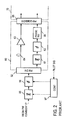
- a feedforward amplifier with improved stabilization and distortion compensation capabilities is disclosed, for example, in Japanese Patent Application Laid-Open Gazette No. 2000-353923.
- the feedforward amplifier is a modification of the prior art example of Fig. 1. As shown in Fig. 2, the variable attenuator 61, the variable phase shifter 62 and the delay line 64 of the first auxiliary amplifier distortion detection circuit in Fig.
- a variable attenuator 55 and the a variable phase shifter 56 are provided immediately preceding the first amplifier distortion detection circuit 60; and a pilot signal introduced between stages of the main amplifier 14 is extracted by a directional coupler from the feedforward amplifier output (the output from the power combiner 53) and is detected by a pilot signal detector and controlled by a controller 97 so that its detected level is minimized.
- variable attenuator 61 and the variable phase shifter 62 on the input side of the first auxiliary amplifier 63 are shared by the distortion elimination circuit 50 and the first auxiliary amplifier distortion detection circuit 60.
- the balance of the distortion elimination circuit 50 is achieved, the balance of the first auxiliary amplifier distortion detection circuit 60 cannot be reached.
- the feedforward amplifier with a dual loop according to the present invention comprises:
- the loop balance of the first auxiliary amplifier distortion detection circuit is controlled by the variable attenuator and the variable phase shifter inserted in the input path of the first auxiliary amplifier and the loop balance of the distortion elimination circuit is controlled by the variable attenuator and the variable phase shifter inserted in the input path of the first auxiliary amplifier distortion detection circuit.
- Fig. 3 illustrates in block form a first embodiment of the feedforward amplifier according to the present invention, which uses three pilot signals and four control means.
- the feedforward amplifier of this embodiment has the distortion detection circuit 10 and the distortion elimination circuit 50, and with a view to canceling the distortion produced by the first auxiliary amplifier 63 of the distortion elimination circuit 50, the first auxiliary amplifier 63 is feedforward-configured by providing the first auxiliary amplifier distortion detection circuit 60 and the first auxiliary amplifier distortion elimination circuit 70 in the distortion injection path 10D.
- the distortion detection circuit 10 comprises: the power divider 11 for dividing the amplifier input signal to the main amplifier signal path 10A and the linear signal transfer path 10B; the first variable attenuator 12, the variable phase shifter 13 and the main amplifier 14 inserted in the main amplifier signal path 10A; the delay line 15 and the phase inverter circuit 16 forming the linear signal transfer path 10B; and the power combiner/divider 17 which combines the outputs from the two paths 10A and 10B and then divides the combined output to two paths.
- the signals divided by the power combiner/divider 17 are input to the delay line 51 forming the main signal transfer path 10C and the distortion injection path 10D in the distortion elimination circuit 50.
- the distortion injection circuit 10D there are inserted in the distortion injection circuit 10D a directional coupler 82, a second variable attenuator 55, a second variable phase shifter 56, the first auxiliary amplifier distortion detection circuit 60, the first auxiliary amplifier distortion elimination circuit 70 and a directional coupler 84.
- the first auxiliary amplifier distortion detection circuit 60 comprises: the power divider 52 for dividing the output from the second variable phase shifter 56 to the first auxiliary amplifier signal transfer path 16E and the first auxiliary amplifier linear signal transfer path 16F; a fourth variable attenuator 61, a fourth variable phase shifter 62 and the first auxiliary amplifier 63 inserted in the first auxiliary amplifier signal transfer path 16E; the delay line 64 and the phase inverter circuit 63 forming the first auxiliary amplifier linear signal transfer path 16F; and the power combiner/divider 66 for combining the outputs from the two paths 16E and 16F and then dividing the combined output to two paths.
- the first auxiliary amplifier distortion elimination circuit 70 comprises: the first auxiliary amplifier main signal path 17G which is formed by the delay line and supplied with one of the two signals divided by the power combiner/divider 66; the first auxiliary amplifier distortion injection path 17H which is formed by a directional coupler 73, a third variable attenuator 72 and a third variable phases shifter 73 and is supplied with the other divided signal from the power combiner/divider 66; and the power combiner 76 which combines the outputs from the paths 17G and 17H and provides the combined output via the directional coupler 84 to the power combiner 53.
- a first pilot signal generator 86 for generating a first pilot signal
- a directional coupler 81 provided on the input side of the power divider 11 for introducing the first pilot signal into the input thereto
- a second pilot signal generator 87 for generating and introducing a second pilot signal into between stages of the main amplifier 14
- a third pilot signal generator 88 for generating and introducing a third pilot signal into between stages of the first auxiliary amplifier 63.
- a first pilot signal detector 91 for detecting the level of the first pilot signal extracted via the directional coupler 82 and a first controller 96 supplied with the detected level, for controlling the first variable attenuator 12 and the first variable phase shifter 13 to minimize the detected signal level.
- a second pilot signal detector 94-1 for detecting the level of the second pilot signal extracted via the directional coupler 75 and a fourth controller 99 for controlling the fourth variable attenuator 61 and the fourth variable phase shifter 62 to minimize the detected signal level.
- a second pilot signal detector 92-1 for detecting the level of the second pilot signal extracted via a directional coupler 85 and a second controller 97 for controlling the second variable attenuator 55 and the second variable phase shifter 56 to minimize the detected signal level.
- the present invention by controlling the variable attenuator 55 and the variable phase shifter 56 inserted in series in the distortion injection path 10D of the distortion elimination circuit 50 which is the input path to the first auxiliary amplifier distortion detection circuit 60, it is possible to effect balance control of the loop of the distortion elimination circuit 50 without affecting the balance of the loop of the first auxiliary amplifier distortion detection circuit 60. Besides, since the balance control of the loop of the first auxiliary amplifier distortion detection circuit 60 is performed by the fourth variable attenuator 61 and the fourth variable phase shifter 62 inserted in the same signal transfer path as that in which the first auxiliary amplifier 63 is inserted, there is no need for such a wide range of variation as is required for the variable attenuator 61 and the variable phase shifter 62 in the Fig. 2 prior art example.
- the feedforward amplifier of the Fig. 3 embodiment brings the distortion detection circuit 10, the first auxiliary amplifier distortion detection circuit 60, the first auxiliary amplifier distortion elimination circuit 70 and the distortion elimination circuit 50 into balance by use of three pilot signals. That is, the feedforward amplifier establishes the balance of the loop of the distortion detection circuit 10 by applying the first pilot signal to the first variable attenuator 12 and the first variable phase shifter 13 to control them and the balance of the loop of the first auxiliary amplifier distortion detection circuit 60 by applying the second pilot signal to the fourth variable attenuator 61 and the fourth phase shifter 62 to control them.
- the balance of the loop of the distortion elimination circuit 50 is established by applying the second pilot signal to the second variable attenuator 55 and the second variable phase shifter 56 to control them after the loop of the first auxiliary amplifier distortion detection circuit 60 is brought into balance.
- the balance of the loop of the first auxiliary amplifier distortion elimination circuit 70 can be acquired by applying the third pilot signal to the third variable attenuator 72 and th third variable phase shifter 73 to control them. In this way, the respective loops of the distortion elimination circuit and the first auxiliary amplifier distortion detection circuit are brought into balance.
- the third variable attenuator 72 and the third variable phase shifter 73 can be adjusted at any stage of the balance adjustment for the other loops.
- Fig. 4 illustrates in block form a second embodiment of the feedforward amplifier according to the present invention, which is configured to use four pilot signals and four control means. While in the Fig. 3 embodiment the second pilot signal is used in common to the adjustment of the second variable attenuator 55 and the second variable phase shifter 56 and the adjustment of the fourth variable attenuator 61 and the fourth variable phase shifter 62, the Fig. 4 embodiment generates a fourth pilot signal dedicated to the adjustment of the fourth variable attenuator 61 and the fourth variable phase shifter 62, and introduces the fourth pilot signal into the input side of the first auxiliary amplifier distortion detection circuit 60.
- a directional coupler 83 is inserted in the distortion injection path 10D on the input side of the first auxiliary amplifier distortion detection circuit 60 and the fourth pilot signal generated by a fourth pilot signal generator 89 is provided via the directional coupler 83 to the first auxiliary amplifier distortion detection circuit 60. Further, the fourth pilot signal is extracted via the directional coupler 75 of the first auxiliary amplifier distortion elimination circuit 70, then the level of the fourth pilot signal is detected by a fourth pilot signal detector 94-2, and based on the detected level, the fourth variable attenuator 61 and the variable phase shifter 62 are controlled by the fourth controller 99. Since this arrangement is the same as in the Fig. 3 embodiment, no description will be repeated.
- variable attenuators and the variable phase shifters in the embodiments of Figs. 3 and 4 usually have characteristics that the attenuation and the phase shift amount monotonously increase as control voltages V Att and V Ph increase as depicted in Figs. 5A and 5B.
- the relationships among control voltages V Att and V Ph for the variable attenuator and the variable phase shifter and the level V L of the pilot signal detected by the pilot signal detector is expressed by a surface of revolution (hereinafter referred to as a paraboloid of revolution) formed by revolving a substantially parabolic curve about a straight line parallel to the V L -axis on three orthogonal coordinates V Att , V Ph and V L as shown in Fig. 6.
- the phase shift amount control voltage V Ph is fixed at an arbitrary value, and on a parabola formed by cutting the paraboloid of revolution by a plane vertical to the V Ph -axis passing through the fixed value of the phase shift amount control voltage V Ph , the attenuation control voltage V Att is changed in a direction in which to decrease the detected pilot signal level V L and is fixed, and on a parabola formed by cutting the paraboloid of revolution by a plane vertical to the V Att -axis passing through the fixed value of the attenuation control voltage V Att , the phase shift amount control voltage V Ph is changed in a direction in which to decrease in the detected pilot signal level V L .
- Such a procedure is repeated and the balance control is discontinued at the time when the detected pilot signal level V L goes down below a reference value.
- the detected pilot signal level at which the distortion component in the transmission signal becomes lower than a predetermined value is set as a reference voltage V R , and a difference voltage V L -V R between the detected pilot signal level V L and the reference voltage V R is applied as the attenuation control voltage V Att and the phase shift amount control voltage V Ph from the control circuit to the variable attenuator and the variable phase shifter to effect their feedback control, and the control voltages are fixed at voltage values at the time the difference voltage V L -V R is reduced to zero.
- the controllers can also be implemented by a single controller which controls the variable attenuators and the variable phase shifters on a time-division basis. This controller sharing contributes to the reduction of power consumption.
- the control algorithm may be such a conventional application algorithm as a perturbation method or least square estimation method.
- the balance of the loop of the feedforward amplifier changes, in general, with a variation in the power supply voltage or device temperature. The change speed of the loop balance to time is relatively low. Hence, a control algorithm, even if consuming much time for convergence to an optimum value, can sufficiently deal with control of the feedforward amplifier with a dual loop according to the present invention.
- the pilot signals may be non-modulated or modulated waves set to different frequencies, or waves set to the same frequency but spread by different spreading codes.
- a pilot signal detector for detected the non-modulated pilot signal is formed using a narrow-band level detector. For example, a band-pass filter for limits the pass band of the detected signal and a diode or similar level detector are used for the pilot signal detector.
- a pilot signal detector for detecting the modulated pilot signal is formed by a frequency converter for frequency converting the detected pilot signal to a base band signal and a demodulator for demodulating the frequency-converted base band signal.
- a pilot signal detector for detecting the spread pilot signal is made up of a frequency converter for down-converting the pilot signal to a base band signal, a de-spreader for de-spreading the base band signal, and a demodulator for demodulating the de-spread signal.
- the automatic adjustment scheme for the feedforward amplifier according to the present invention is applicable to various pilot signals.
- Various pilot signal generators and pilot signal detectors applicable to the feedforward amplifier of the present invention are described, for example, in US Patent No. 6,208,204.
- Fig. 7 depicts the principal part of an arrangement which does not use the second pilot signal in the embodiments of Figs. 3 and 4.
- the second signal generator 87 in Figs. 3 and 4 is not provided and the second pilot signal detector 92-2 replaced with an error signal detection circuit 100, and based on the detected error signal, the second controller 97 controls the second variable attenuator 55 and the second variable phase shifter 56.
- the error detection circuit 100 in this example comprises a demodulator 101, low-pass filters 102 and 103 to which IQ signals are demodulated input signal in the demodulator 101, analog-digital converters 104 and 105, and an error signal detector 106.
- the transmission signal containing distortion components is extracted by the directional coupler 85, from which it is provided to the demodulator 101.
- the demodulator 101 simultaneously detects the transmission signal and distortion components produced due to the nonlinear characteristic of the main amplifier 14, and outputs in-phase (I) and quadrature (Q) signals.
- the low-pass filters 102 and 103 eliminate high-frequency components from input signal components to the analog-digital converters 104 and 105.
- the analog-digital converters 104 and 105 convert the band-limited I and Q signals to digital form. This embodiment has been described to use the analog-digital converters 104 and 105 since it performs the error signal detection by digital signal processing, but in the case of using an analog signal for the error signal detection, the analog-digital converters 104 and 105 are unnecessary.
- the error signal detector 106 decides the transmission signal containing nonlinear components. For example, when the transmission signal is a QPSK-modulated signal, the error detector 106 detects, as an error signal E S indicating the distortion component in the transmitting signal, the difference between a correct transmission signal point P S and a demodulated signal point P R as depicted in Fig. 8A, then generates a correcting signal C S of a vector equal in absolute value to the detected error signal E S in a direction opposite thereto as shown in Fig. 8B, and provides the correcting signal C S as I and Q components I(C S ) and Q(C S ) to the controller 97.
- the controller 97 amplitude/phase converts the correcting signal to generate an amplitude control signal V Att as a control signal for the variable attenuator 55 and a phase control signal V Ph as a control signal for the variable phase shifter 56.
- the amplitude control signal V Att is calculated by a square root, (I(C S ) 2 +Q(C S ) 2 ) 1/2 , of the sum of squares of the signals I(C S ) signal and Q(C S ) provided from the error signal detector 106.
- the phase control signal V Ph is calculated by tan -1 (Q(C S )/I(C S )) from the signals I(C S ) and Q(C S ) provided from the error signal detector 106.
- the first auxiliary amplifier distortion elimination circuit 70 in Figs. 3 and 4 can also be configured to control the third variable attenuator 72 and the third variable phase shifter 73 without using the third pilot signal.
- a distortion cancellation signal produced by the distortion injection path 10D supplied with the distortion components generated by the first auxiliary amplifier 63, is extracted by the directional coupler 84, and the extracted distortion cancellation signal is subjected to demodulation by the error signal detection circuit 100 to generate correcting signals I(C S ) and Q(C S ), which are provided to the controller 98, which, in turn, controls the third variable attenuator 72 and the third variable phase shifter 73 based on the correcting signals I(C S ) and Q(C S ).
- both of the distortion elimination circuit 50 and the first auxiliary amplifier distortion elimination circuit 70 can also be configured to use the demodulation scheme described above with reference to Fig. 7.
- the controllers 96 to 99 each control the respective pair of variable attenuator and variable phase shifter to minimize the detected pilot signal level or IQ-demodulated distortion component; in practice, each controller compares a predetermined reference level and the detected pilot signal level, and controls the variable attenuator and the variable phase shifter 56 on a stepwise basis until the pilot signal level goes down below the reference level.
- a control algorithm can be implemented by the conventional perturbation method, least square estimation method or the like.
- the controllers 96 to 99 may each be formed by a digital processing unit using a microprocessor or an analog calculation circuit. In either case, it is preferable from the viewpoint of efficient balance control that the balance control of the loop of the distortion elimination circuit 50 be preceded by the balance control of the loop of the first auxiliary amplifier distortion detection circuit 60, but balance control of the other loops (the loops of the distortion detection circuit 10 and the first auxiliary amplifier distortion elimination circuit 70) may be at any desired stages of processing. This somewhat impairs the efficiency of balance control, but allows each of the controllers 96 to 99 to effect the balance control independently of the others.
- the feedforward amplifier of the first embodiment of the present invention described above is a feedforward amplifier with a dual loop which is provided with a distortion detection circuit for detecting a nonlinear distortion produced by a main amplifier and a distortion elimination circuit which amplifies the detected distortion component by a first auxiliary amplifier and then introduces the amplified distortion components into the output from said main amplifier, said distortion elimination circuit being formed by a first auxiliary amplifier distortion detection circuit for detecting a nonlinear distortion produced by said first auxiliary amplifier of said distortion elimination circuit and a first auxiliary amplifier distortion elimination circuit which amplifies the distortion component detected by said first auxiliary amplifier distortion detection circuit and then introduces the amplified distortion component into the output from said first auxiliary amplifier to cancel the distortion component generated by said first auxiliary amplifier, said feedforward amplifier comprising:
- the feedforward amplifier of the second embodiment of the present invention described above is a feedforward amplifier with a dual loop which is provided with a distortion detection circuit for detecting a nonlinear distortion produced by a main amplifier and a distortion elimination circuit which amplifies the detected distortion component by a first auxiliary amplifier and then introduces the amplified distortion components into the output from said main amplifier, said distortion elimination circuit being formed by a first auxiliary amplifier distortion detection circuit for detecting a nonlinear distortion produced by said first auxiliary amplifier of said distortion elimination circuit and a first auxiliary amplifier distortion elimination circuit which amplifies the distortion component detected by said first auxiliary amplifier distortion detection circuit and then introduces the amplified distortion component into the output from said first auxiliary amplifier to cancel the distortion component generated by said first auxiliary amplifier, said feedforward amplifier comprising:
- the feedforward amplifier with a dual loop permits implementation of balance control of the loop of the distortion elimination circuit 50 without affecting the balance of the loop of the first auxiliary amplifier distortion detection circuit 60 by controlling the variable attenuator 55 and the variable phase shifter 56 inserted in series in the input path to the first auxiliary amplifier distortion detection circuit in the distortion injection path 10D of the distortion elimination circuit 50.
- the present invention provides the following advantages over the prior art.
Landscapes
- Physics & Mathematics (AREA)
- Nonlinear Science (AREA)
- Engineering & Computer Science (AREA)
- Power Engineering (AREA)
- Amplifiers (AREA)
Applications Claiming Priority (2)
| Application Number | Priority Date | Filing Date | Title |
|---|---|---|---|
| JP2001340534 | 2001-11-06 | ||
| JP2001340534 | 2001-11-06 |
Publications (2)
| Publication Number | Publication Date |
|---|---|
| EP1309082A2 true EP1309082A2 (de) | 2003-05-07 |
| EP1309082A3 EP1309082A3 (de) | 2004-01-07 |
Family
ID=19154714
Family Applications (1)
| Application Number | Title | Priority Date | Filing Date |
|---|---|---|---|
| EP02024636A Ceased EP1309082A3 (de) | 2001-11-06 | 2002-11-05 | Vorwärtsgekoppelter Verstärker mit doppelter schleife |
Country Status (5)
| Country | Link |
|---|---|
| US (1) | US6838934B2 (de) |
| EP (1) | EP1309082A3 (de) |
| KR (1) | KR100612741B1 (de) |
| CN (1) | CN1215727C (de) |
| SG (1) | SG124247A1 (de) |
Cited By (3)
| Publication number | Priority date | Publication date | Assignee | Title |
|---|---|---|---|---|
| EP1684416A1 (de) * | 2005-01-19 | 2006-07-26 | Northrop Grumman Corporation | Methode zur Verringerung von Intermodulationsprodukten eines Feedforward-Verstärkers unter Verwendung eines gering verzerrenden Verstärkers |
| EP2178206A2 (de) | 2008-10-17 | 2010-04-21 | Fraunhofer-Gesellschaft zur Förderung der angewandten Forschung e.V. | Feed-forward-Verstärker mit Vorrichtung zum Erzeugen eines Korrektursignals |
| WO2021167508A1 (en) * | 2020-02-21 | 2021-08-26 | Telefonaktiebolaget Lm Ericsson (Publ) | A feedforward amplifier |
Families Citing this family (9)
| Publication number | Priority date | Publication date | Assignee | Title |
|---|---|---|---|---|
| US6452366B1 (en) * | 2000-02-11 | 2002-09-17 | Champion Microelectronic Corp. | Low power mode and feedback arrangement for a switching power converter |
| JP3910167B2 (ja) * | 2003-09-25 | 2007-04-25 | 松下電器産業株式会社 | 増幅回路 |
| EP1560328B1 (de) * | 2004-01-28 | 2010-09-15 | NTT DoCoMo, Inc. | Mehrfachband-Vorwärtskopplungsverstärker und Methode zur Einstellung desselben |
| US7091781B2 (en) * | 2004-10-29 | 2006-08-15 | Motorola, Inc. | Wideband feed forward linear power amplifier |
| CN100576767C (zh) * | 2005-06-03 | 2009-12-30 | 株式会社Ntt都科摩 | 多频带用前馈放大器 |
| DE602006000131T2 (de) * | 2005-06-03 | 2008-07-03 | Ntt Docomo Inc. | Bandauswahl-Vorwärtskopplungsverstärker |
| JP2008270851A (ja) * | 2007-04-16 | 2008-11-06 | Hitachi Kokusai Electric Inc | フィードフォワード増幅器 |
| KR102204678B1 (ko) | 2014-12-11 | 2021-01-20 | 삼성전자주식회사 | 인버터 증폭기 기반의 이중 루프 레귤레이터 및 그에 따른 전압 레귤레이팅 방법 |
| CN115941057B (zh) * | 2023-03-15 | 2023-06-02 | 北京航空航天大学 | 一种具有误差提取和均衡功能的微波光子正交解调装置 |
Family Cites Families (12)
| Publication number | Priority date | Publication date | Assignee | Title |
|---|---|---|---|---|
| US5304945A (en) * | 1993-04-19 | 1994-04-19 | At&T Bell Laboratories | Low-distortion feed-forward amplifier |
| JPH0777330A (ja) | 1993-09-06 | 1995-03-20 | Harman Co Ltd | 加熱調理器 |
| KR100266817B1 (ko) * | 1997-01-31 | 2000-09-15 | 윤종용 | 피드포워드방식의선형증폭장치및방법 |
| US5977826A (en) * | 1998-03-13 | 1999-11-02 | Behan; Scott T. | Cascaded error correction in a feed forward amplifier |
| US6166600A (en) * | 1998-08-31 | 2000-12-26 | Lucent Technologies Inc. | Automatic gain and phase controlled feedforward amplifier without pilot signal |
| US6127889A (en) * | 1998-11-18 | 2000-10-03 | Lucent Technologies Inc. | Nested feed forward distortion reduction system |
| JP3827130B2 (ja) | 1999-03-31 | 2006-09-27 | 株式会社エヌ・ティ・ティ・ドコモ | フィードフォワード増幅器 |
| JP3613447B2 (ja) | 1999-06-10 | 2005-01-26 | 株式会社エヌ・ティ・ティ・ドコモ | 二重ループを持つフィードフォワード増幅器 |
| US6320464B1 (en) * | 1999-03-13 | 2001-11-20 | Ntt Mobile Communications Network, Inc. | Feedforward amplifier |
| US6320461B1 (en) * | 2000-05-12 | 2001-11-20 | Jhong Sam Lee | Ultra-linear feedforward RF power amplifier |
| JP2001339251A (ja) * | 2000-05-25 | 2001-12-07 | Mitsubishi Electric Corp | フィードフォワード増幅器 |
| KR20020056877A (ko) | 2000-05-25 | 2002-07-10 | 롤페스 요하네스 게라투스 알베르투스 | 로직 회로, 푸시 풀 증폭기, 로직 상태의 시퀀스 수행방법 및 핸드셰이킹 방법 |
-
2002
- 2002-11-04 CN CNB021503265A patent/CN1215727C/zh not_active Expired - Fee Related
- 2002-11-05 SG SG200206661A patent/SG124247A1/en unknown
- 2002-11-05 EP EP02024636A patent/EP1309082A3/de not_active Ceased
- 2002-11-05 US US10/287,681 patent/US6838934B2/en not_active Expired - Fee Related
- 2002-11-06 KR KR1020020068324A patent/KR100612741B1/ko not_active Expired - Fee Related
Cited By (7)
| Publication number | Priority date | Publication date | Assignee | Title |
|---|---|---|---|---|
| EP1684416A1 (de) * | 2005-01-19 | 2006-07-26 | Northrop Grumman Corporation | Methode zur Verringerung von Intermodulationsprodukten eines Feedforward-Verstärkers unter Verwendung eines gering verzerrenden Verstärkers |
| US7308234B2 (en) | 2005-01-19 | 2007-12-11 | Northrop Grumman Corporation | Feedforward spur cancellation approach using low IP amplifier |
| EP2178206A2 (de) | 2008-10-17 | 2010-04-21 | Fraunhofer-Gesellschaft zur Förderung der angewandten Forschung e.V. | Feed-forward-Verstärker mit Vorrichtung zum Erzeugen eines Korrektursignals |
| DE102008052172A1 (de) | 2008-10-17 | 2010-04-22 | Fraunhofer-Gesellschaft zur Förderung der angewandten Forschung e.V. | Vorrichtung zum Erzeugen eines Korrektursignals |
| US7940106B2 (en) | 2008-10-17 | 2011-05-10 | Fraunhofer-Gesellschaft Zur Foerderung Der Angewandten Forschung E.V. | Apparatus for generating a correction signal |
| WO2021167508A1 (en) * | 2020-02-21 | 2021-08-26 | Telefonaktiebolaget Lm Ericsson (Publ) | A feedforward amplifier |
| US12334871B2 (en) | 2020-02-21 | 2025-06-17 | Telefonaktiebolaget Lm Ericsson (Publ) | Feedforward amplifier |
Also Published As
| Publication number | Publication date |
|---|---|
| CN1215727C (zh) | 2005-08-17 |
| CN1444411A (zh) | 2003-09-24 |
| US6838934B2 (en) | 2005-01-04 |
| KR20030038444A (ko) | 2003-05-16 |
| EP1309082A3 (de) | 2004-01-07 |
| US20030085759A1 (en) | 2003-05-08 |
| KR100612741B1 (ko) | 2006-08-18 |
| SG124247A1 (en) | 2006-08-30 |
Similar Documents
| Publication | Publication Date | Title |
|---|---|---|
| US5770971A (en) | Distortion compensation control for a power amplifier | |
| US5789976A (en) | Digital adaptive control of feedforward amplifier using frequency domain cancellation | |
| US7058368B2 (en) | Adaptive feedforward noise cancellation circuit | |
| JP3880329B2 (ja) | ループゲイン制御方法及び電力増幅回路 | |
| US7693497B2 (en) | Spurious energy correlation for control of linear power amplifiers | |
| EP1158661A2 (de) | Vorwärtsgekoppelter Verstärker | |
| KR100438445B1 (ko) | 비선형 왜곡 보상 방법 및 비선형 왜곡 보상 회로 | |
| US6838934B2 (en) | Feedforward amplifier with dual loop | |
| US5831478A (en) | Feedforward amplifier | |
| WO1996030997A1 (en) | Feed forward rf amplifier | |
| US6081156A (en) | Method and apparatus for amplifying feedforward linear power using pilot tone hopping | |
| US5396189A (en) | Adaptive feedback system | |
| CA2265143A1 (en) | Technique for effectively rendering power amplification and control in wireless communications | |
| US7088968B2 (en) | Method and polar-loop transmitter with origin offset for zero-crossing signals | |
| JPH10511534A (ja) | 無線周波数通信システムにおいて使用する増幅回路および増幅器の制御方法 | |
| WO1993019521A1 (fr) | Amplificateur a correction aval | |
| EP0905919B1 (de) | System und Verfahren zur Kalibrierung nichtlinearer Verstärker | |
| EP1381155A2 (de) | Ein Leistungsverstärkergerät mit Verzerrungskompensation und Verfahren dazu | |
| CN1158824C (zh) | 一种线性功率放大方法及其装置 | |
| US6545487B1 (en) | System and method for producing an amplified signal with reduced distortion | |
| EP1193860B1 (de) | Vorwärtsgekoppelte Linearisierer | |
| US6608523B1 (en) | System and method for producing a pilot signal in a distortion reduction system | |
| JP3613447B2 (ja) | 二重ループを持つフィードフォワード増幅器 | |
| JP2000244341A (ja) | カーテシアン・フィードバック回路における飽和防止回路 | |
| JP2000013254A (ja) | 無線機 |
Legal Events
| Date | Code | Title | Description |
|---|---|---|---|
| PUAI | Public reference made under article 153(3) epc to a published international application that has entered the european phase |
Free format text: ORIGINAL CODE: 0009012 |
|
| 17P | Request for examination filed |
Effective date: 20021105 |
|
| AK | Designated contracting states |
Designated state(s): AT BE BG CH CY CZ DE DK EE ES FI FR GB GR IE IT LI LU MC NL PT SE SK TR |
|
| AX | Request for extension of the european patent |
Extension state: AL LT LV MK RO SI |
|
| PUAL | Search report despatched |
Free format text: ORIGINAL CODE: 0009013 |
|
| AK | Designated contracting states |
Kind code of ref document: A3 Designated state(s): AT BE BG CH CY CZ DE DK EE ES FI FR GB GR IE IT LI LU MC NL PT SE SK TR |
|
| AX | Request for extension of the european patent |
Extension state: AL LT LV MK RO SI |
|
| 17Q | First examination report despatched |
Effective date: 20040206 |
|
| AKX | Designation fees paid |
Designated state(s): DE GB IT |
|
| STAA | Information on the status of an ep patent application or granted ep patent |
Free format text: STATUS: THE APPLICATION HAS BEEN REFUSED |
|
| 18R | Application refused |
Effective date: 20060405 |