EP1309975B1 - Supraleitendes kabel - Google Patents
Supraleitendes kabel Download PDFInfo
- Publication number
- EP1309975B1 EP1309975B1 EP01958047A EP01958047A EP1309975B1 EP 1309975 B1 EP1309975 B1 EP 1309975B1 EP 01958047 A EP01958047 A EP 01958047A EP 01958047 A EP01958047 A EP 01958047A EP 1309975 B1 EP1309975 B1 EP 1309975B1
- Authority
- EP
- European Patent Office
- Prior art keywords
- superconducting
- tapes
- superconducting material
- layer
- conductor element
- Prior art date
- Legal status (The legal status is an assumption and is not a legal conclusion. Google has not performed a legal analysis and makes no representation as to the accuracy of the status listed.)
- Expired - Lifetime
Links
Images


Classifications
-
- H—ELECTRICITY
- H01—ELECTRIC ELEMENTS
- H01B—CABLES; CONDUCTORS; INSULATORS; SELECTION OF MATERIALS FOR THEIR CONDUCTIVE, INSULATING OR DIELECTRIC PROPERTIES
- H01B12/00—Superconductive or hyperconductive conductors, cables, or transmission lines
- H01B12/02—Superconductive or hyperconductive conductors, cables, or transmission lines characterised by their form
- H01B12/06—Films or wires on bases or cores
-
- Y—GENERAL TAGGING OF NEW TECHNOLOGICAL DEVELOPMENTS; GENERAL TAGGING OF CROSS-SECTIONAL TECHNOLOGIES SPANNING OVER SEVERAL SECTIONS OF THE IPC; TECHNICAL SUBJECTS COVERED BY FORMER USPC CROSS-REFERENCE ART COLLECTIONS [XRACs] AND DIGESTS
- Y02—TECHNOLOGIES OR APPLICATIONS FOR MITIGATION OR ADAPTATION AGAINST CLIMATE CHANGE
- Y02E—REDUCTION OF GREENHOUSE GAS [GHG] EMISSIONS, RELATED TO ENERGY GENERATION, TRANSMISSION OR DISTRIBUTION
- Y02E40/00—Technologies for an efficient electrical power generation, transmission or distribution
- Y02E40/60—Superconducting electric elements or equipment; Power systems integrating superconducting elements or equipment
-
- Y—GENERAL TAGGING OF NEW TECHNOLOGICAL DEVELOPMENTS; GENERAL TAGGING OF CROSS-SECTIONAL TECHNOLOGIES SPANNING OVER SEVERAL SECTIONS OF THE IPC; TECHNICAL SUBJECTS COVERED BY FORMER USPC CROSS-REFERENCE ART COLLECTIONS [XRACs] AND DIGESTS
- Y10—TECHNICAL SUBJECTS COVERED BY FORMER USPC
- Y10S—TECHNICAL SUBJECTS COVERED BY FORMER USPC CROSS-REFERENCE ART COLLECTIONS [XRACs] AND DIGESTS
- Y10S428/00—Stock material or miscellaneous articles
- Y10S428/922—Static electricity metal bleed-off metallic stock
- Y10S428/9265—Special properties
- Y10S428/93—Electric superconducting
Definitions
- the present invention relates in general to superconducting cables, that is to say cables intended for transporting electric current in so-called superconductivity conditions, namely in conditions of almost zero electrical resistance in the regime of transportation of direct current.
- the invention relates to a method for reducing alternating current (AC) losses in a superconducting conductor element subjected to an external magnetic field and through which a current flows. Furthermore, the invention relates to a superconducting conductor element. Furthermore, the invention relates to a superconducting phase element. Furthermore, the invention relates to a warm dielectric superconducting cable.
- AC alternating current
- superconducting conductor element is meant to indicate the electrically active portion of a superconducting cable, comprising a support and at least one layer of superconducting material, intended for transporting the phase electric current or, in the case of a three-phase current, each phase current.
- superconducting phase element is meant to indicate each component of a superconducting cable associated with the or each phase, comprising a superconducting conductor element and the respective electrical and thermal insulations.
- WD warm dielectric
- a superconducting phase element comprising, essentially, a tubular axial support and at least one layer comprising superconducting material (that is to say a superconducting conductor element), a cryostat and a dielectric, wherein a fluid, typically liquid nitrogen, flows within the support element for cooling the superconducting material below its critical temperature.
- superconducting material is meant to indicate a material, as for example special niobium-titanium alloys, or ceramics based on mixed oxides of copper, barium and yttrium (YBCO) or of gadolinium, samarium or other rare earth (REBCO), or of bismuth, lead, strontium, calcium, copper, thallium and mercury (BSCCO), one of which phases has, below a certain temperature defined as critical temperature (T c ), an almost zero resistivity, in the regime of transportation of direct current.
- YBCO yttrium
- REBCO rare earth
- BSCCO critical temperature
- the superconducting material is commonly used in the form of tapes wound around a substantially tubular support element. Tapes containing a film of superconducting material (YBCO or REBCO) supported by a steel tape, optionally coated with one or more layers of oxide, and tapes wherein filaments of superconducting material (BSCCO) are embedded in a metallic matrix are well-known.
- YBCO or REBCO superconducting material
- BSCCO superconducting material
- transport current is meant to indicate a current flowing in a tape comprising superconducting material, in a superconducting conductor element, in a superconducting phase element, or in a superconducting cable, according to the circumstances.
- the losses in a superconducting material are essentially of a hysteretic nature, due to the intrinsic dissipation of the superconducting material caused by the penetration of a magnetic field within the superconducting material itself.
- the losses of a hysteretic nature are added to the losses due to eddy currents, that is to say ohmic losses of the currents which are induced, by variable magnetic fields, in the metallic areas of the superconducting cable in general.
- a first magnetic field causing losses is that generated by the transport current itself. This magnetic field is commonly referred to as "self-field”.
- polyphase cable is meant to indicate a cable wherein the current of each phase, in a single phase or three-phase current system, is distributed among various superconducting phase elements.
- critical current density
- the z-stack configuration is studied, i.e. an infinite series of strips placed with the wide faces adjacent and spaced out and the x-array configuration, i.e. an infinite series of strips placed with the narrow faces adjacent and spaced out.
- a zero gap is an ideal condition, difficult to put into practice.
- it is exceedingly difficult to wind the superconducting tapes with continuity.
- a gap still remains (in the order of about 0.6 mm) between the superconducting material of adjacent tapes, due to the presence of an edge area of the metallic matrix which is free of superconducting filaments.
- the spacing of the superconducting tapes according to the present invention has the further advantage of facilitating machine production of the superconducting phase element.
- the invention relates to a method for reducing the AC losses in a superconducting conductor element subjected to an external magnetic field and through which a current flows, comprising the steps of:
- the value of the gap between the superconducting material of adjacent tapes is chosen by taking into account the opposing requirements of maximizing it to reduce the AC losses and of minimizing it to increase the quantity of transport current, with the same geometry of the superconducting conductor element.
- the predetermined minimum value is 1.2 millimetres.
- the minimum value of the gap is 1.4 millimetres, even more preferably it is 2 millimetres.
- the invention in a second aspect, relates to a superconducting conductor element, comprising at least one layer of tapes comprising superconducting material around a substantially tubular support element, the tapes of each layer being mutually spaced out, characterised in that the tapes of each layer are at such a mutual distance that the gap between the superconducting material of adjacent tapes is not smaller than 1.2 millimetres.
- the tapes comprising a superconducting material are arranged in a number of layers between 2 and 10.
- a layer of a material suitable for facilitating the sliding between the layers of tapes may be placed, for example carbon paper or TYVEK TM .
- the gap between the superconducting material of the different pairs of adjacent tapes may be constant.
- the gap between the superconducting material of adjacent tapes may vary from one layer to another.
- the tapes comprising superconducting material of each layer are helically wound around the support element, at a respective predetermined winding angle - with respect to the longitudinal direction of the support element - preferably between 5° and 50°, more preferably between 8° and 40°. This measure allows for a reduction in any possible mechanical stress of the tapes themselves.
- the gap in each layer may in this case be chosen, from the ranges of values specified above, in such a way as to minimize the difference in critical current between the various layers of tapes comprising superconducting material.
- the tapes comprising superconducting material of at least two adjacent tapes are helically wound in opposite directions.
- the tapes comprising superconducting material are of metallic matrix/multifilament type, as are obtained by the well-known "Powder-in-tube” process and as explained in more detail herebelow.
- filaments of superconducting material those defined above with the initials BSCCO can be conveniently used.
- the superconducting material is the mixed oxide called BSCCO-2223 or Bi-2223.
- the metallic matrix is preferably made from silver, gold or suitable alloys thereof with other metals.
- the tapes can be further partially or totally coated with a metal layer, preferably of steel or a copper-beryllium alloy.
- the tapes comprise a superconducting material in the form of a film, for example those defined above with the initials YBCO or REBCO. These, for example, are prepared as described in US 5,741,377 to Martin Marietta Co.
- the invention in a third aspect, relates to a warm dielectric superconducting phase element comprising a superconducting conductor element as described above, a cryostat coaxially external to it, and a dielectric coaxially external to the cryostat.
- the superconducting phase element of the invention is cooled down by means of a suitable pressurized or undercooled cooling fluid, in order to ensure the heat exchange necessary for its operation and to guarantee that a temperature suitably below the critical temperature of the superconducting material is maintained, even for a phase element of a long length.
- the cooling fluid is simultaneously subjected to progressive heating, as a result of the heat released as a consequence of the losses of the various components, and to a progressive loss in pressure, due to hydraulic losses while flowing through the phase element and to the more or less turbulent flow of the fluid itself.
- the superconducting material is of the so-called high temperature type (T c in the order of about 100K) and is cooled down to a temperature between about 63K and 90K.
- T c high temperature type
- Such cooling if preferably achieved using liquid nitrogen as the cooling fluid, at a working pressure between 5 and 25 bar.
- the cooling fluid is circulated within the substantially tubular support element.
- the invention in a fourth aspect, relates to a warm dielectric superconducting cable comprising at least one superconducting phase element as described.
- said superconducting cable is a three-phase cable.
- a three-phase warm dielectric superconducting cable 1 comprises a superconducting core, globally indicated by 2, comprising a plurality of superconducting phase elements 3, indicated by 3a, 3b, 3c, housed, preferably loosely, within a tubular containing case 11, for example of a metallic material, such as steel, copper, aluminium or the like.
- the tubular containing case 11 is preferably formed from a tape wound in tubular form and longitudinally welded, or from an extruded tube or similar. Whenever the demands for flexibility of the cable so require, this may be corrugated.
- Each of the phase elements 3 comprises a superconducting conductor element 31 comprising a substantially tubular support element 4 and, coaxially upon it, at least one layer 5 comprising superconducting material (described in detail below).
- Each of the phase elements 3 further comprises, coaxially external to the superconducting conductor element 31: a cryostat made up of a first corrugated tube 6, a thermal insulator 7 and a second corrugated tube 8; a dielectric 9; a metallic shield 10; and spacers 10'.
- the cryostat 6-8 having the purpose of minimizing outward thermal dispersion, comprises a thermal insulator 7 formed, for example, by a plurality of superimposed layers, and at least one protection sheath.
- the thermal insulator 7 is, for example, made up of several surface-metallized tapes (for example some tens) made from a polyester resin, known in the field as "thermal super-insulator", loosely wound, possibly with the aid of interposed spacers (not shown).
- cable 1 comprises a cooling circuit for circulating a cooling fluid suitable for cooling the superconducting material to a temperature suitably below its critical temperature.
- a cooling fluid suitable for cooling the superconducting material to a temperature suitably below its critical temperature.
- such superconducting material is preferably of high temperature type, that is to say having a critical temperature T c in the order of about 110K.
- the above-mentioned cooling circuit comprises suitable pumping means, well-known per se and therefore not shown, intended for supplying a suitable cooling fluid, for example liquid nitrogen, at a temperature typically between 65 and 90K, within the substantially tubular support elements 4 of each of the superconducting conductor elements 31, as indicated by arrows RF.
- a suitable cooling fluid for example liquid nitrogen
- the tubular containing case 11 may be filled with gas or oil 12 at a pressure, for example, of 13.8 bars, in order to lubricate and increase the performance of dielectric 9.
- the tubular containing case 11 is furthermore preferably coated with an external sheath 13, for example made of polyethylene.
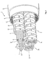
- FIG. 1 shows the superconducting conductor element 31, in perspective and not to scale, wherein the support element 4 is schematized.
- Layers 14 and 15, just like any other superconducting layer that may be present, are preferably separated by a layer 16 of a material suitable for promoting the sliding between the layers, for example carbon paper or TYVEK TM .
- Each superconducting layer 14, 15 is in turn made up of a plurality of tapes 17 helically wound according to a respective winding angle ⁇ , ⁇ .
- the winding angles of each superconducting layer may vary as described above.
- winding directions and angles of the tapes 17 of the various layers may be equal or different, but preferably at least two adjacent layers are provided comprising tapes wound in opposite directions, as superconducting layers 14, 15 shown in Figure 2.
- the tapes 17 of a same superconducting layer are reciprocally spaced out. This distance has been indicated by D for the tapes 17 of superconducting layer 14 and by D' for the tapes 17 of superconducting layer 15.
- the distance D (and D') is indicated in the cross direction of the tapes themselves, i.e. on the circumference C 2 illustrated, which forms together with the circumference C 1 illustrated, perpendicular to the axis A-A of the phase element, an angle ⁇ equal to the winding angle of the tapes 17.
- the distance between adjacent tapes may be constant or vary from one layer to the other.
- Figure 3 shows a diagrammatic cross-section of the superconducting conductor element 31, taken along a portion of circumference C 2 in Figure 2.
- the portion of circumference is illustrated as rectilinear in virtue of the high ratio between the transverse size (width W) of each tape 17a-17e and the radius of curvature of the support element 4.
- thickness T of the tapes is also indicated.
- the thickness T is much less than the width W, that is to say that the tapes 17 comprising superconducting material have a high aspect ratio.
- the width of the tapes 17 of each layer 14, 15 may, furthermore, be the same or different.
- the tapes 17a-17b of the embodiment shown in Figure 3 are of metallic matrix/multifilament type, obtained by the process known as "Powder-in-Tube" (PIT).
- PIT Powder-in-Tube
- This process essentially involves pressing a powder precursor of the superconducting material, for example the above-mentioned BSCCO material, in a tube made of silver, silver alloy or other noble metal. The tube is subsequently deformed by drawing or rolling and thermally treated to convert the powder precursor into the superconducting material.
- the resulting section which can be seen from Figure 3, appears as substantially rectangular and comprises a metallic "matrix" 18, in the internal portion whereof the superconducting material 19 is concentrated in the form of a plurality of filaments of a substantially rectangular cross-section and distributed in a substantially irregular manner.
- two edges 18a, 18b are formed of a metallic matrix substantially free of superconducting filaments 19.
- the superconducting material 19 of two adjacent tapes 17, for example of the tapes 17a, 17b shown, are therefore spaced out by a gap indicated by G, greater than the above-mentioned distance D.
- the tapes 17 may, furthermore, be partially or totally coated with a metallic layer (not shown), for example of steel or a copper-beryllium alloy.
- the superconducting conductor element comprised a tubular support having a diameter of 30.2 millimetres, upon which 63 BSCCO-2223/Ag tapes, supplied by the American Superconductor Corporation, Westborough, MA, U.S.A., were wound by hand in four layers.
- the tapes used of the type marketed as "Wide”, had a width of 4.1 ⁇ 0.1 mm and a silver matrix thickness of 0.215 mm, and were coated on the main faces with a steel sheet, to a total thickness of 0.32 mm.
- the distance between adjacent tapes of each layer was of 1.4 mm. Such a distance, considering the transverse size of the metallic edges of the silver matrix, corresponded to a gap between the superconducting material of adjacent tapes, as defined above, of 2 millimetres.
- the total critical current measured turned out to be 4750 ⁇ 100 A, with a degradation with respect to the calculated value ( ⁇ I c /I c ) of -21%.
- the current distribution resulted to be uniform among the layers.
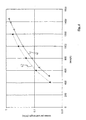
- Figures 4 and 5 graphically show the measurement results.
- Figure 4 shows the patterns of the total losses within the superconducting conductor element as a function of the root-mean-square value of the transport current in the superconducting conductor element
- Figure 5 shows the patterns of the losses per unit length of the tape comprising superconducting material as a function of the root-mean-square value of the transport current per tape.
- lines 41 and 51 illustrate the measured values and the approximate curves of the losses in three-phase configuration, at a temperature of 76K and a frequency of 60Hz.
- a superconducting conductor element comprising a tubular support with a diameter of 30.2 mm, upon which 86 BSCCO-2223/Ag tapes, supplied by the American Superconductor Corporation, Westborough, MA, U.S.A., were wound, by hand and in four layers. There were 20, 23, 23 and 20 tapes, helically wound at winding angles equal to those of the Example 1.
- the distance between adjacent tapes of each layer was of 0.1 mm. Such a distance, considering the transverse size of the metallic edge of the silver matrix, corresponded to a gap, as defined above, of 0.7 mm.
- the tapes used had a width of 4.0 ⁇ 0.1 mm and a silver matrix thickness of 0.205 mm and were coated on the main faces with a steel sheet, to a total thickness of 0.32 mm.
- the measured total critical current turned out to be 5400 ⁇ 500 A, with a degradation with respect to the calculated value of -18%.
- the current distribution turned out to be uniform among the layers.
- lines 42 and 52 illustrate the measured values and the approximate curves of the losses in three-phase configuration, at a temperature of 76K and a frequency of 60Hz.
- Example 1 (Invention)
- Example 2 (Comparison) Diameter of support element (mm) 30.2 30.2 Winding angles -29.5°/-13°/ 13°/38° -29.5°/-13°/ 13°/38° Number of layers 4 4 Measured total I c (A) ⁇ I c /I c 4750 ⁇ 100 -21% 5400 ⁇ 500 -18% Tape width (mm)/thickness (mm) 4.1/0.32 4.0/0.32 Number of tapes: total and per layer 63 15/17/17/14 86 20/23/23/20 Average I c per tape (A) 95.5 76.5 Calculated total I c (A) 6000 6600 Distance between tapes (mm) 1.4 0.1 Gap (mm) 2 0.7
- the parameters considered to be essential in order to evaluate the AC losses are the following: diameter of the support element, winding angles of the layers, measured total critical current and thickness of the layers, it can be seen that the superconducting conductor elements of Table I exhibited characteristics that, to the above mentioned purposes, are substantially similar.
- such a superconducting conductor element according to the invention may advantageously be used in various configurations of a superconducting cable.
- the measuring conditions in three-phase configuration followed in the Examples can be compared not only to the working conditions of each superconducting phase element in a three-phase cable, but also to the working conditions in a single-phase cable subjected to external magnetic fields, such as for example a single-phase cable placed near to a generator, an engine, a current limiter etc.
Landscapes
- Superconductors And Manufacturing Methods Therefor (AREA)
Claims (18)
- Verfahren zum Verringern von Wechselstromverlusten in einem supraleitenden Leiterelement (31), das einem externen Magnetfeld ausgesetzt ist, und durch welches ein Strom fließt, mit folgenden Schrittena) Bereitstellung eines im wesentlichen rohrförmigen Halterungselements (4),b) Anordnen mehrerer Bänder (17), die supraleitendes Material in zumindest einer Schicht (5; 14, 15) aufweisen, um das Halterungselement (4) herum, wobei die Bänder (17) jeder Schicht auf einer derartigen gegenseitigen Entfernung (D) gehaltert werden, dass der Spalt (G) zwischen dem supraleitenden Material (19) benachbarter Bänder (17a, 17b) nicht kleiner ist als ein vorbestimmter Minimalwert.
- Verfahren nach Anspruch 1, dadurch gekennzeichnet, dass der vorbestimmte Minimalwert 1,2 mm beträgt.
- Verfahren nach Anspruch 2, dadurch gekennzeichnet, dass der vorbestimmte Minimalwert 1,4 mm beträgt.
- Verfahren nach Anspruch 3, dadurch gekennzeichnet, dass der vorbestimmte Minimalwert 2 mm beträgt.
- Verfahren nach einem der voranstehenden Ansprüche, dadurch gekennzeichnet, dass die Bänder (17), die supraleitendes Material aufweisen, in einer Anzahl von Schichten zwischen zwei und zehn vorgesehen sind.
- Verfahren nach Anspruch 5, dadurch gekennzeichnet, dass der Schritt (b) des Anordnens der Bänder (17) so durchgeführt wird, dass helixförmig die Bänder (17) jeder Schicht (14, 15) um das Halterungselement (4) gewickelt werden, wobei die Bänder (17) von zumindest zwei benachbarten Schichten (14, 15) in entgegengesetzten Richtungen gewickelt werden.
- Verfahren nach einem der voranstehenden Ansprüche, dadurch gekennzeichnet, dass die Bänder (17), die supraleitendes Material aufweisen, vom Metallmatrix/Multifilament-Typ sind.
- Verfahren nach einem der voranstehenden Ansprüche, dadurch gekennzeichnet, dass das supraleitende Material vom BSCCO-Typ ist.
- Supraleitendes Leiterelement (31), das zumindest eine Schicht (5; 14, 15) aus Bändern (17) aufweist, die supraleitendes Material aufweisen, das um ein im wesentliches rohrförmiges Halterungselement (4) herum angeordnet ist, wobei die Bänder (17) jeder Schicht (5, 14, 15) voneinander beabstandet sind, dadurch gekennzeichnet, dass die Bänder (17) eine derartige gegenseitige Entfernung (D, D') aufweisen, dass der Spalt (G) zwischen dem supraleitenden Material (19) benachbarter Bänder (17a, 17b) nicht kleiner ist als 1,2 mm.
- Supraleitendes Leiterelement (31) nach Anspruch 9, dadurch gekennzeichnet, dass der Spalt (G) einen vorbestimmten Minimalwert von 1,4 mm aufweist.
- Supraleitendes Leiterelement (31) nach Anspruch 9, dadurch gekennzeichnet, dass der Spalt (G) einen vorbestimmten Minimalwert von 2 mm aufweist.
- Supraleitendes Leiterelement (31) nach einem der Ansprüche 9 bis 11, dadurch gekennzeichnet, dass zwei bis zehn Schichten (14, 15) aus Bändern (17) vorgesehen sind, die supraleitendes Material aufweisen.
- Supraleitendes Leiterelement nach Anspruch 12, dadurch gekennzeichnet, dass die Bänder (17) jeder Schicht (14, 15) helixförmig um das Halterungselement (4) gewickelt sind, wobei die Bänder (17) zumindest zweier benachbarter Schichten (14, 15) in entgegengesetzten Richtungen gewickelt sind.
- Supraleitendes Leiterelement nach einem der Ansprüche 9 bis 13, dadurch gekennzeichnet, dass die Bänder (17), die supraleitendes Material aufweisen, vom Metallmatrix/Multifilament-Typ sind.
- Supraleitendes Leiterelement nach Anspruch 14, dadurch gekennzeichnet, dass das supraleitende Material vom BSCCO-Typ ist.
- Element (3a, 3b, 3c) mit einer supraleitenden Phase und einem warmen Dielektrikum, das ein supraleitendes Leiterelement (31) nach einem der Ansprüche 9 bis 15 aufweist.
- Supraleitendes Kabel (1) mit warmem Dielektrikum, das zumindest ein Element (3a, 3b, 3c) mit einer supraleitenden Phase nach Anspruch 16 aufweist.
- Supraleitendes Kabel (1) nach Anspruch 17, dadurch gekennzeichnet, dass es ein Dreiphasen-Kabel ist.
Priority Applications (1)
| Application Number | Priority Date | Filing Date | Title |
|---|---|---|---|
| EP01958047A EP1309975B1 (de) | 2000-08-14 | 2001-08-02 | Supraleitendes kabel |
Applications Claiming Priority (6)
| Application Number | Priority Date | Filing Date | Title |
|---|---|---|---|
| EP00202854 | 2000-08-14 | ||
| EP00202854 | 2000-08-14 | ||
| US22530800P | 2000-08-15 | 2000-08-15 | |
| US225308P | 2000-08-15 | ||
| PCT/EP2001/008950 WO2002015203A1 (en) | 2000-08-14 | 2001-08-02 | Superconducting cable |
| EP01958047A EP1309975B1 (de) | 2000-08-14 | 2001-08-02 | Supraleitendes kabel |
Publications (2)
| Publication Number | Publication Date |
|---|---|
| EP1309975A1 EP1309975A1 (de) | 2003-05-14 |
| EP1309975B1 true EP1309975B1 (de) | 2005-04-13 |
Family
ID=56290177
Family Applications (1)
| Application Number | Title | Priority Date | Filing Date |
|---|---|---|---|
| EP01958047A Expired - Lifetime EP1309975B1 (de) | 2000-08-14 | 2001-08-02 | Supraleitendes kabel |
Country Status (6)
| Country | Link |
|---|---|
| EP (1) | EP1309975B1 (de) |
| AT (1) | ATE293280T1 (de) |
| AU (1) | AU2001279800A1 (de) |
| DE (1) | DE60110090T2 (de) |
| ES (1) | ES2240490T3 (de) |
| WO (1) | WO2002015203A1 (de) |
Families Citing this family (7)
| Publication number | Priority date | Publication date | Assignee | Title |
|---|---|---|---|---|
| JP2003141946A (ja) * | 2001-11-02 | 2003-05-16 | Sumitomo Electric Ind Ltd | 超電導ケーブル |
| US6745059B2 (en) * | 2001-11-28 | 2004-06-01 | American Superconductor Corporation | Superconductor cables and magnetic devices |
| US7608785B2 (en) | 2004-04-27 | 2009-10-27 | Superpower, Inc. | System for transmitting current including magnetically decoupled superconducting conductors |
| ES2334616A1 (es) * | 2008-02-04 | 2010-03-12 | Universidade De Santiago De Compostela | Limitador superconductor de corriente integrado en el intercambiador de calor de un refrigerador termoacustico. |
| CN103004046B (zh) | 2011-01-27 | 2017-09-05 | 古河电气工业株式会社 | 超导电缆的终端连接部 |
| US8938278B2 (en) | 2011-02-18 | 2015-01-20 | The Regents Of The University Of Colorado | Superconducting cables and methods of making the same |
| CN104029821B (zh) * | 2013-10-11 | 2015-03-11 | 中国人民解放军空军济南航空四站装备修理厂 | 飞机地面空调电源动力综合保障设备 |
Family Cites Families (3)
| Publication number | Priority date | Publication date | Assignee | Title |
|---|---|---|---|---|
| DE2318617A1 (de) * | 1973-04-13 | 1974-11-07 | Kabel Metallwerke Ghh | Elektrisches tieftemperaturkabel |
| JP3541123B2 (ja) * | 1998-03-16 | 2004-07-07 | 日本原子力研究所 | 超伝導電流リード |
| CN1331831A (zh) * | 1998-12-24 | 2002-01-16 | 皮雷利·卡维系统有限公司 | 超导电缆 |
-
2001
- 2001-08-02 ES ES01958047T patent/ES2240490T3/es not_active Expired - Lifetime
- 2001-08-02 AU AU2001279800A patent/AU2001279800A1/en not_active Abandoned
- 2001-08-02 WO PCT/EP2001/008950 patent/WO2002015203A1/en not_active Ceased
- 2001-08-02 AT AT01958047T patent/ATE293280T1/de not_active IP Right Cessation
- 2001-08-02 EP EP01958047A patent/EP1309975B1/de not_active Expired - Lifetime
- 2001-08-02 DE DE60110090T patent/DE60110090T2/de not_active Expired - Lifetime
Also Published As
| Publication number | Publication date |
|---|---|
| ES2240490T3 (es) | 2005-10-16 |
| DE60110090T2 (de) | 2006-03-09 |
| DE60110090D1 (de) | 2005-05-19 |
| AU2001279800A1 (en) | 2002-02-25 |
| WO2002015203A1 (en) | 2002-02-21 |
| EP1309975A1 (de) | 2003-05-14 |
| ATE293280T1 (de) | 2005-04-15 |
Similar Documents
| Publication | Publication Date | Title |
|---|---|---|
| Carr et al. | Filamentary YBCO conductors for AC applications | |
| CA2772158C (en) | Multifilament conductor and method for its production | |
| Wolf et al. | HTS CroCo: A stacked HTS conductor optimized for high currents and long-length production | |
| EP0786783B1 (de) | Verfahren zur Leitung eines vorgegebenen Stroms durch ein supraleitendes Hochleistungskabel | |
| EP1016095B1 (de) | Fehlerstrom limitierende supraleitende spule | |
| EP0650205A1 (de) | Supraleitender Kabelleiter | |
| EP1441366B1 (de) | Supraleitendes kabel und supraleitende kabelleitung | |
| JPH09511098A (ja) | 超電導磁気コイル | |
| KR20120089568A (ko) | 초전도 케이블 및 교류 송전 케이블 | |
| US7091423B2 (en) | Superconducting cable | |
| EP1147524B1 (de) | Supraleitendes kabel | |
| WO1998047155A1 (en) | Low resistance cabled conductors comprising superconducting ceramics | |
| US6985761B2 (en) | Superconducting cable | |
| WO2002025672A2 (en) | Superconducting cable | |
| EP1309975B1 (de) | Supraleitendes kabel | |
| US6759593B2 (en) | Superconducting cable | |
| Herrmann et al. | Development of twisted Bi-2212 and Bi-2223 powder in tube conductors for ac applications | |
| Hayashi et al. | Development of Ag-sheathed Bi2223 superconducting wires and their application to magnets | |
| EP1205945B1 (de) | Supraleitendes Kabel | |
| Lacaze et al. | Coils performances of superconducting cables for 50/60 Hz applications | |
| Carr Jr et al. | Possibilities for use of coated superconductors in AC applications | |
| Scanlan et al. | Multifilamentary Nb 3 Sn for superconducting generator applications | |
| JP3585719B2 (ja) | 酸化物超電導ケーブルユニットおよびそれを備えた酸化物超電導ケーブル | |
| Savvides et al. | Critical current and magnetic field performance of Bi-2223/Ag composite superconducting tapes | |
| Bortnik et al. | Investigations on the development of superconducting DC power transmission lines |
Legal Events
| Date | Code | Title | Description |
|---|---|---|---|
| PUAI | Public reference made under article 153(3) epc to a published international application that has entered the european phase |
Free format text: ORIGINAL CODE: 0009012 |
|
| 17P | Request for examination filed |
Effective date: 20030214 |
|
| AK | Designated contracting states |
Designated state(s): AT BE CH CY DE DK ES FI FR GB GR IE IT LI LU MC NL PT SE TR |
|
| AX | Request for extension of the european patent |
Extension state: AL LT LV MK RO SI |
|
| RAP1 | Party data changed (applicant data changed or rights of an application transferred) |
Owner name: PIRELLI S.P.A. |
|
| RAP1 | Party data changed (applicant data changed or rights of an application transferred) |
Owner name: PIRELLI & C. S.P.A. |
|
| GRAP | Despatch of communication of intention to grant a patent |
Free format text: ORIGINAL CODE: EPIDOSNIGR1 |
|
| GRAS | Grant fee paid |
Free format text: ORIGINAL CODE: EPIDOSNIGR3 |
|
| GRAA | (expected) grant |
Free format text: ORIGINAL CODE: 0009210 |
|
| AK | Designated contracting states |
Kind code of ref document: B1 Designated state(s): AT BE CH CY DE DK ES FI FR GB GR IE IT LI LU MC NL PT SE TR |
|
| PG25 | Lapsed in a contracting state [announced via postgrant information from national office to epo] |
Ref country code: TR Free format text: LAPSE BECAUSE OF FAILURE TO SUBMIT A TRANSLATION OF THE DESCRIPTION OR TO PAY THE FEE WITHIN THE PRESCRIBED TIME-LIMIT Effective date: 20050413 Ref country code: AT Free format text: LAPSE BECAUSE OF FAILURE TO SUBMIT A TRANSLATION OF THE DESCRIPTION OR TO PAY THE FEE WITHIN THE PRESCRIBED TIME-LIMIT Effective date: 20050413 Ref country code: CH Free format text: LAPSE BECAUSE OF FAILURE TO SUBMIT A TRANSLATION OF THE DESCRIPTION OR TO PAY THE FEE WITHIN THE PRESCRIBED TIME-LIMIT Effective date: 20050413 Ref country code: NL Free format text: LAPSE BECAUSE OF FAILURE TO SUBMIT A TRANSLATION OF THE DESCRIPTION OR TO PAY THE FEE WITHIN THE PRESCRIBED TIME-LIMIT Effective date: 20050413 Ref country code: FI Free format text: LAPSE BECAUSE OF FAILURE TO SUBMIT A TRANSLATION OF THE DESCRIPTION OR TO PAY THE FEE WITHIN THE PRESCRIBED TIME-LIMIT Effective date: 20050413 Ref country code: BE Free format text: LAPSE BECAUSE OF FAILURE TO SUBMIT A TRANSLATION OF THE DESCRIPTION OR TO PAY THE FEE WITHIN THE PRESCRIBED TIME-LIMIT Effective date: 20050413 Ref country code: LI Free format text: LAPSE BECAUSE OF FAILURE TO SUBMIT A TRANSLATION OF THE DESCRIPTION OR TO PAY THE FEE WITHIN THE PRESCRIBED TIME-LIMIT Effective date: 20050413 |
|
| REG | Reference to a national code |
Ref country code: GB Ref legal event code: FG4D |
|
| REG | Reference to a national code |
Ref country code: CH Ref legal event code: EP |
|
| REG | Reference to a national code |
Ref country code: IE Ref legal event code: FG4D |
|
| REF | Corresponds to: |
Ref document number: 60110090 Country of ref document: DE Date of ref document: 20050519 Kind code of ref document: P |
|
| PG25 | Lapsed in a contracting state [announced via postgrant information from national office to epo] |
Ref country code: SE Free format text: LAPSE BECAUSE OF FAILURE TO SUBMIT A TRANSLATION OF THE DESCRIPTION OR TO PAY THE FEE WITHIN THE PRESCRIBED TIME-LIMIT Effective date: 20050713 Ref country code: GR Free format text: LAPSE BECAUSE OF FAILURE TO SUBMIT A TRANSLATION OF THE DESCRIPTION OR TO PAY THE FEE WITHIN THE PRESCRIBED TIME-LIMIT Effective date: 20050713 Ref country code: DK Free format text: LAPSE BECAUSE OF FAILURE TO SUBMIT A TRANSLATION OF THE DESCRIPTION OR TO PAY THE FEE WITHIN THE PRESCRIBED TIME-LIMIT Effective date: 20050713 |
|
| PG25 | Lapsed in a contracting state [announced via postgrant information from national office to epo] |
Ref country code: CY Free format text: LAPSE BECAUSE OF FAILURE TO SUBMIT A TRANSLATION OF THE DESCRIPTION OR TO PAY THE FEE WITHIN THE PRESCRIBED TIME-LIMIT Effective date: 20050802 Ref country code: IE Free format text: LAPSE BECAUSE OF NON-PAYMENT OF DUE FEES Effective date: 20050802 Ref country code: LU Free format text: LAPSE BECAUSE OF NON-PAYMENT OF DUE FEES Effective date: 20050802 |
|
| PG25 | Lapsed in a contracting state [announced via postgrant information from national office to epo] |
Ref country code: MC Free format text: LAPSE BECAUSE OF NON-PAYMENT OF DUE FEES Effective date: 20050831 |
|
| PG25 | Lapsed in a contracting state [announced via postgrant information from national office to epo] |
Ref country code: PT Free format text: LAPSE BECAUSE OF FAILURE TO SUBMIT A TRANSLATION OF THE DESCRIPTION OR TO PAY THE FEE WITHIN THE PRESCRIBED TIME-LIMIT Effective date: 20050913 |
|
| NLV1 | Nl: lapsed or annulled due to failure to fulfill the requirements of art. 29p and 29m of the patents act | ||
| REG | Reference to a national code |
Ref country code: ES Ref legal event code: FG2A Ref document number: 2240490 Country of ref document: ES Kind code of ref document: T3 |
|
| REG | Reference to a national code |
Ref country code: CH Ref legal event code: PL |
|
| PLBE | No opposition filed within time limit |
Free format text: ORIGINAL CODE: 0009261 |
|
| STAA | Information on the status of an ep patent application or granted ep patent |
Free format text: STATUS: NO OPPOSITION FILED WITHIN TIME LIMIT |
|
| ET | Fr: translation filed | ||
| 26N | No opposition filed |
Effective date: 20060116 |
|
| REG | Reference to a national code |
Ref country code: IE Ref legal event code: MM4A |
|
| REG | Reference to a national code |
Ref country code: FR Ref legal event code: CD Ref country code: FR Ref legal event code: TP |
|
| REG | Reference to a national code |
Ref country code: GB Ref legal event code: 732E |
|
| REG | Reference to a national code |
Ref country code: GB Ref legal event code: 732E |
|
| REG | Reference to a national code |
Ref country code: ES Ref legal event code: PC2A |
|
| PGFP | Annual fee paid to national office [announced via postgrant information from national office to epo] |
Ref country code: ES Payment date: 20100826 Year of fee payment: 10 |
|
| REG | Reference to a national code |
Ref country code: ES Ref legal event code: FD2A Effective date: 20130610 |
|
| PG25 | Lapsed in a contracting state [announced via postgrant information from national office to epo] |
Ref country code: ES Free format text: LAPSE BECAUSE OF NON-PAYMENT OF DUE FEES Effective date: 20110803 |
|
| PGFP | Annual fee paid to national office [announced via postgrant information from national office to epo] |
Ref country code: DE Payment date: 20140827 Year of fee payment: 14 |
|
| PGFP | Annual fee paid to national office [announced via postgrant information from national office to epo] |
Ref country code: GB Payment date: 20140827 Year of fee payment: 14 Ref country code: FR Payment date: 20140818 Year of fee payment: 14 |
|
| PGFP | Annual fee paid to national office [announced via postgrant information from national office to epo] |
Ref country code: IT Payment date: 20140823 Year of fee payment: 14 |
|
| REG | Reference to a national code |
Ref country code: DE Ref legal event code: R119 Ref document number: 60110090 Country of ref document: DE |
|
| GBPC | Gb: european patent ceased through non-payment of renewal fee |
Effective date: 20150802 |
|
| PG25 | Lapsed in a contracting state [announced via postgrant information from national office to epo] |
Ref country code: IT Free format text: LAPSE BECAUSE OF NON-PAYMENT OF DUE FEES Effective date: 20150802 |
|
| REG | Reference to a national code |
Ref country code: FR Ref legal event code: ST Effective date: 20160429 |
|
| PG25 | Lapsed in a contracting state [announced via postgrant information from national office to epo] |
Ref country code: DE Free format text: LAPSE BECAUSE OF NON-PAYMENT OF DUE FEES Effective date: 20160301 Ref country code: GB Free format text: LAPSE BECAUSE OF NON-PAYMENT OF DUE FEES Effective date: 20150802 |
|
| PG25 | Lapsed in a contracting state [announced via postgrant information from national office to epo] |
Ref country code: FR Free format text: LAPSE BECAUSE OF NON-PAYMENT OF DUE FEES Effective date: 20150831 |