EP1310014B1 - Drahtloses funkgerät - Google Patents
Drahtloses funkgerät Download PDFInfo
- Publication number
- EP1310014B1 EP1310014B1 EP01954054A EP01954054A EP1310014B1 EP 1310014 B1 EP1310014 B1 EP 1310014B1 EP 01954054 A EP01954054 A EP 01954054A EP 01954054 A EP01954054 A EP 01954054A EP 1310014 B1 EP1310014 B1 EP 1310014B1
- Authority
- EP
- European Patent Office
- Prior art keywords
- antenna
- handset
- ground conductor
- impedance
- terminal
- Prior art date
- Legal status (The legal status is an assumption and is not a legal conclusion. Google has not performed a legal analysis and makes no representation as to the accuracy of the status listed.)
- Expired - Lifetime
Links
- 239000004020 conductor Substances 0.000 claims abstract description 18
- 239000003990 capacitor Substances 0.000 claims abstract description 16
- 238000010168 coupling process Methods 0.000 claims abstract description 15
- 238000005859 coupling reaction Methods 0.000 claims abstract description 15
- 230000008878 coupling Effects 0.000 claims abstract description 12
- 230000001965 increasing effect Effects 0.000 abstract description 4
- 238000012986 modification Methods 0.000 abstract description 4
- 230000004048 modification Effects 0.000 abstract description 4
- 229910052751 metal Inorganic materials 0.000 description 13
- 239000002184 metal Substances 0.000 description 12
- 238000012360 testing method Methods 0.000 description 9
- 238000004088 simulation Methods 0.000 description 7
- 230000005855 radiation Effects 0.000 description 6
- 238000013461 design Methods 0.000 description 3
- 230000001939 inductive effect Effects 0.000 description 3
- 230000005540 biological transmission Effects 0.000 description 2
- 230000001413 cellular effect Effects 0.000 description 2
- 238000000926 separation method Methods 0.000 description 2
- 239000000758 substrate Substances 0.000 description 2
- RYGMFSIKBFXOCR-UHFFFAOYSA-N Copper Chemical compound [Cu] RYGMFSIKBFXOCR-UHFFFAOYSA-N 0.000 description 1
- WYTGDNHDOZPMIW-RCBQFDQVSA-N alstonine Natural products C1=CC2=C3C=CC=CC3=NC2=C2N1C[C@H]1[C@H](C)OC=C(C(=O)OC)[C@H]1C2 WYTGDNHDOZPMIW-RCBQFDQVSA-N 0.000 description 1
- 230000009286 beneficial effect Effects 0.000 description 1
- 238000004891 communication Methods 0.000 description 1
- 229910052802 copper Inorganic materials 0.000 description 1
- 239000010949 copper Substances 0.000 description 1
- 230000003247 decreasing effect Effects 0.000 description 1
- 230000009977 dual effect Effects 0.000 description 1
- 230000000694 effects Effects 0.000 description 1
- 238000003780 insertion Methods 0.000 description 1
- 230000037431 insertion Effects 0.000 description 1
- 238000004519 manufacturing process Methods 0.000 description 1
- 238000001465 metallisation Methods 0.000 description 1
- 238000000034 method Methods 0.000 description 1
- 230000005404 monopole Effects 0.000 description 1
- 230000003287 optical effect Effects 0.000 description 1
- 229920003023 plastic Polymers 0.000 description 1
- 239000004033 plastic Substances 0.000 description 1
- 238000004904 shortening Methods 0.000 description 1
- 239000007787 solid Substances 0.000 description 1
- 125000006850 spacer group Chemical group 0.000 description 1
Images





Classifications
-
- H—ELECTRICITY
- H01—ELECTRIC ELEMENTS
- H01Q—ANTENNAS, i.e. RADIO AERIALS
- H01Q1/00—Details of, or arrangements associated with, antennas
- H01Q1/12—Supports; Mounting means
- H01Q1/22—Supports; Mounting means by structural association with other equipment or articles
- H01Q1/24—Supports; Mounting means by structural association with other equipment or articles with receiving set
- H01Q1/241—Supports; Mounting means by structural association with other equipment or articles with receiving set used in mobile communications, e.g. GSM
- H01Q1/242—Supports; Mounting means by structural association with other equipment or articles with receiving set used in mobile communications, e.g. GSM specially adapted for hand-held use
- H01Q1/243—Supports; Mounting means by structural association with other equipment or articles with receiving set used in mobile communications, e.g. GSM specially adapted for hand-held use with built-in antennas
-
- H—ELECTRICITY
- H01—ELECTRIC ELEMENTS
- H01Q—ANTENNAS, i.e. RADIO AERIALS
- H01Q9/00—Electrically-short antennas having dimensions not more than twice the operating wavelength and consisting of conductive active radiating elements
- H01Q9/04—Resonant antennas
- H01Q9/30—Resonant antennas with feed to end of elongated active element, e.g. unipole
- H01Q9/40—Element having extended radiating surface
-
- H—ELECTRICITY
- H01—ELECTRIC ELEMENTS
- H01Q—ANTENNAS, i.e. RADIO AERIALS
- H01Q9/00—Electrically-short antennas having dimensions not more than twice the operating wavelength and consisting of conductive active radiating elements
- H01Q9/04—Resonant antennas
- H01Q9/30—Resonant antennas with feed to end of elongated active element, e.g. unipole
- H01Q9/42—Resonant antennas with feed to end of elongated active element, e.g. unipole with folded element, the folded parts being spaced apart a small fraction of the operating wavelength
Definitions
- the present invention relates to a wireless terminal, for example a mobile phone handset.
- Wireless terminals such as mobile phone handsets, typically incorporate either an external antenna, such as a normal mode helix or meander line antenna, or an internal antenna, such as a Planar Inverted-F Antenna (PIFA) or similar. Examples of different internal and external antennas are given below.
- an external antenna such as a normal mode helix or meander line antenna
- an internal antenna such as a Planar Inverted-F Antenna (PIFA) or similar. Examples of different internal and external antennas are given below.
- PIFA Planar Inverted-F Antenna
- Patent Specification GB-A-2344969 discloses a mobile phone comprising a clam shell case formed by an upper part which is connected by hinges to a lower part.
- An antenna comprises a metallised layer on the upper part and a metal sheet on the lower part.
- a switch electrically interconnects the upper and lower parts in the normal, open position in which signals can be received and transmitted and isolates these parts electrically in the standby, closed position in which only signals can be received.
- the antenna arrangement In the standby position the antenna arrangement is a planar one in which the metallised layer in the upper part is the antenna and the metal layer in the lower part is the ground plane.
- the antenna In the normal position the antenna is a monopole antenna.
- Patent Specification US-A-4,723,305 discloses a dual band notch antenna for portable radiotelephones. Two embodiments are described, each located in the lower part of the radiotelephone housing.
- respective transmit and receive antenna elements are parallel arranged metal rods having for example a length of one fifteenth of the wavelength of their centre design frequency extending lengthwise from a first printed circuit board (PCB) through holes provided in a plastics spacer. At their distal ends they are connected together by a one-half wavelength transmission line in the form a serpentine track provided on a second PCB.
- Respective transmission lines are provided on the first PCB to connect the metal rods to respective transmit and receive filters.
- the filters present a nominal 50 ⁇ reactance at their respective transmit and receive frequencies and a large reactance at the respective receive or transmit frequencies.
- the second embodiment comprises a ⁇ /4 wavelength long notch extending lengthwise from the bottom of the radiotelephone housing. Receive and transmit coaxial cables are connected to opposite ends of the notch to provide wide banding of the notch antenna. The width of the notch determines the operational frequency bandwidth of the notch. A solid dielectric may be provided in the notch.
- Patent Specification EP-A1-0 622 864 discloses a radio apparatus comprising a main housing part containing high, frequency circuitry for the transmitter and receiver and one or more sub-housing parts containing low frequency circuitry including control circuitry.
- the main housing part carries an antenna which may be a rod antenna, microstrip antenna or an inverted F antenna. Lines are provided for interconnecting the circuitry contained within the main housing part and the sub-housing part(s). Measures are taken to suppress RF currents in the lines connecting the circuitry in the main housing part and the sub-housing part(s).
- These measures comprise providing a control element having a reactance component coupling the main housing part and the sub-housing parts; an open stub or stubs on the lines connecting main housing and sub-housing part(s) or using optical fibres to connect circuitry in the main housing part to circuitry in the sub-housing part(s).
- Patent Specification US-A-5,764,190 discloses a capacitively loaded PIFA mounted externally of a handset casing.
- the antenna comprises a planar conductor mounted spaced from, and connected at one end to, a ground plane.
- the other end of the planar conductor forms a capacitive load with the ground plane.
- a capacitive feed is provided by a planar conductive plate disposed between the planar conductor and the ground plane.
- a coaxial cable connects the RF feed to the planar conductive plate.
- Patent Specification WO 99/43039 discloses a substrate antenna comprising a conductive quarter wavelength long trace provided on a nonconductive support substrate which may be a separate entity or be provided by the housing or a surface within a wireless device.
- the trace is disposed within the wireless device at a location adjacent to and beyond an edge of a ground plane.
- Patent Specification US-A-4,491,843 discloses a portable receiver having a dipole antenna for use in a unilateral call system.
- the dipole antenna comprises a parallelepiped metal box containing an amplifier forming part of an input stage of the receiver.
- a metal plate is mounted spaced from one surface of the metal box and is connected by an inductor to one input of the amplifier.
- a second input of the amplifier is connected to the metal box.
- the surface areas of the one surface of the metal box and of the metal plate are substantially equal.
- the metal box functions as a virtual metal plate located halfway up the metal box.
- the inductor serves to match the antenna to the input impedance of the amplifier.
- a further problem with known antenna arrangements for wireless terminals is that they are generally unbalanced, and therefore couple strongly to the terminal case. As a result a significant amount of radiation emanates from the terminal itself rather than the antenna.
- An object of the present invention is to provide a wireless terminal having efficient radiation properties over a wide bandwidth.
- a wireless terminal comprising a ground conductor and a transceiver coupled to an antenna feed, characterised in that the antenna feed is coupled to the ground conductor via a physically very small capacitor having a large capacitance for maximum coupling and minimum reactance, the capacitor being a parallel plate capacitor formed by a conducting plate and a portion of the ground conductor, wherein the ground conductor functions as the radiator of the wireless terminal.
- the present invention is based upon the recognition, not present in the prior art, that the impedances of an antenna and a wireless handset are similar to those of an asymmetric dipole, which are separable, and on the further recognition that the antenna impedance can be replaced with a non-radiating coupling element.
- Figure 1 shows a model of the impedance seen by a transceiver, in transmit mode, in a wireless handset at its antenna feed point.
- the impedance is modelled as an asymmetrical dipole, where the first arm 102 represents the impedance of the antenna and the second arm 104 the impedance of the handset, both arms being driven by a source 106.
- the impedance of such an arrangement is substantially equivalent to the sum of the impedance of each arm 102,104 driven separately against a virtual ground 108.
- the model could equally well be used for reception by replacing the source 106 by an impedance representing that of the transceiver, although this is rather more difficult to simulate.
- the antenna If the size of the antenna is reduced, its radiation resistance R 1 will also reduce. If the antenna becomes infinitesimally small its radiation resistance R 1 will fall to zero and all of the radiation will come from the handset. This situation can be made beneficial if the handset impedance is suitable for the source 106 driving it and if the capacitive reactance of the infinitesimal antenna can be minimised by increasing the capacitive back-coupling to the handset.
- the equivalent circuit is modified to that shown in Figure 4.
- the antenna has therefore been replaced with a physically very small back-coupling capacitor, designed to have a large capacitance for maximum coupling and minimum reactance.
- the residual reactance of the back-coupling capacitor can be tuned out with a simple matching circuit.
- the resulting bandwidth can be much greater than with a conventional antenna and handset combination, because the handset acts as a low Q radiating element (simulations show that a typical Q is around 1), whereas conventional antennas typically have a Q of around 50.
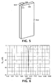
- a basic embodiment of a capacitively back-coupled handset is shown in Figure 5.
- a handset 502 has dimensions of 10 ⁇ 40 ⁇ 100mm, typical of modern cellular handsets.
- a parallel plate capacitor 504, having dimensions 2 ⁇ 10 ⁇ 10mm, is formed by mounting a 10x10mm plate 506 2mm above the top edge 508 of the handset 502, in the position normally occupied by a much larger antenna.
- the resultant capacitance is about 0.5pF, representing a compromise between capacitance (which would be increased by reducing the separation of the handset 502 and plate 504) and coupling effectiveness (which depends on the separation of the handset 502 and plate 504).
- the capacitor is fed via a support 510, which is insulated from the handset case 502.
- the return loss S 11 of this embodiment after matching was simulated using the High Frequency Structure Simulator (HFSS), available from Ansoft Corporation, with the results shown in Figure 6 for frequencies f between 1000 and 2800MHz.
- HFSS High Frequency Structure Simulator
- a conventional two inductor "L” network was used to match at 1900MHz.
- the resultant bandwidth at 7dB return loss (corresponding to approximately 90% of input power radiated) is approximately 60MHz, or 3%, which is useful but not as large as was required.
- a Smith chart illustrating the simulated impedance of this embodiment over the same frequency range is shown in Figure 7.
- Figure 8 shows the resistance variation, over the same frequency range as before, simulated using HFSS. This can be improved by redesigning the case to increase the resistance.
- Figure 9 shows a second embodiment having a narrow capacitively back-coupled handset 902.
- the handset 902 has dimensions of 10 ⁇ 10 ⁇ 100mm, while the dimensions of the capacitor 504, formed from the plate 506 and top surface 908 of the handset 902, and the support 510 are unchanged from the previous embodiment. Simulations were again performed to determine the resistance variation of this embodiment, with the results shown in Figure 10. This clearly demonstrates that use of a narrow handset provides a wider bandwidth where the resistance is higher than that of the basic configuration.
- the length of the handset could be optimised to give a wide bandwidth centred on a particular frequency, by shifting the resonant frequencies of the structure.
- a horizontal slot i.e. a slot across the width of the handset
- electrically shortening or lengthening the handset could be used for the purpose of electrically shortening or lengthening the handset.
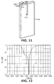
- FIG. 11 shows a third embodiment having a slotted capacitively back-coupled handset 1102, with a 33mm deep slot 1112 in the case, together with a capacitor 504.
- the dimensions of the capacitor 504, formed from the plate 506 and top surface 1108 of the handset 1102, and the support 510 are unchanged from the previous embodiments.
- the presence of the slot 1112 significantly increases the resistance of the case, as seen by the transceiver, in the region of 1900MHz, allowing the low-Q case to be matched to 50 ⁇ without a significant loss of bandwidth.
- the return loss S 11 of this embodiment was again simulated using HFSS, with the results shown in Figure 12 for frequencies f between 1000 and 2800MHz, using a similar two inductor matching network to that used for the basic embodiment.
- the resultant bandwidth at 7dB return loss is greatly improved at approximately 350MHz, or 18%, which is approaching that required to cover UMTS and DCS 1800 bands simultaneously.
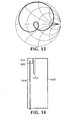
- a Smith chart illustrating the simulated impedance of this embodiment over the same frequency range is shown in Figure 13.
- Figure 14 is a plan view of the test piece, which comprises a copper ground plane 1402 having dimensions 40 ⁇ 100mm on a 0.8mm thick FR4 circuit board (with a measured dielectric constant of 4.1).
- a 3 ⁇ 29.5mm slot 1412 is provided in the ground plane and a 10x10mm plate 506 is located 2mm above the corner of the ground plane 1402.
- the plate and co-extensive portion of the ground plane 1402 form a parallel plate capacitor, as in the embodiments described above.
- the capacitor is fed via a co-axial cable 1404 attached to the rear surface of the circuit board and a vertical pin 510.
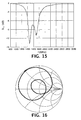
- the return loss S 11 of this embodiment was measured without matching, which was then added in simulations.
- the matching added was a 3.5nH series inductor and a 4nH shunt inductor, similar to that used in the simulations described above. Results are shown in Figure 15 for frequencies f between 800 and 3000MHz.
- the resultant bandwidth at 7dB return loss is approximately 350MHz centred at 1600MHz, or 22%, which is approximately the fractional bandwidth required to cover UMTS and DCS 1800 bands simultaneously.
- a Smith chart illustrating the impedance of this embodiment over the same frequency range is shown in Figure 16.
- any other sacrificial (non-radiating) coupling element could be used instead, for example inductive coupling.
- the coupling element could be altered in order to aid impedance matching.
- capacitive coupling could be achieved via an inductive element which has the advantage of requiring no further matching components.
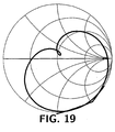
- FIG. 17 As an example of this latter technique a further test piece was produced, illustrated in plan view in Figure 17. This piece is similar to that shown in Figure 14, with the difference that the plate 506 is slightly offset from the corner of the ground plane 1402 and is no longer completely metallised: instead a spiral track 1706 is provided, connected at one end to the feed pin 501. The length of the track 1706 is chosen to provide resonance at the required frequency, approximately 1600MHz in this embodiment. The track 1706 is fed via a stripline 1704 on the rear surface of the circuit board.
- the return loss S 11 of this embodiment was measured without matching. Results are shown in Figure 18 for frequencies f between 800 and 3000MHz. The resultant bandwidth at 7dB return loss is approximately 135MHz centred at 1580MHz, or 9%, and it is believed that this bandwidth could be improved significantly by further optimisation and matching.
- a Smith chart illustrating the impedance of this embodiment over the same frequency range is shown in Figure 19.
- a conducting handset case has been the radiating element.
- other ground conductors in a wireless terminal could perform a similar function. Examples include conductors used for EMC shielding and an area of Printed Circuit Board (PCB) metallisation, for example a ground plane.
- PCB Printed Circuit Board
Landscapes
- Engineering & Computer Science (AREA)
- Computer Networks & Wireless Communication (AREA)
- Transceivers (AREA)
- Support Of Aerials (AREA)
- Details Of Aerials (AREA)
- Telephone Set Structure (AREA)
- Waveguide Aerials (AREA)
- Crystals, And After-Treatments Of Crystals (AREA)
- Reduction Or Emphasis Of Bandwidth Of Signals (AREA)
- Eye Examination Apparatus (AREA)
Claims (5)
- Drahtlos-Endgerät mit einem Erdungsleiter (502, 902, 1102, 1402) und einem mit einer Antennenspeisung (1404, 1704) gekoppelten Transceiver, dadurch gekennzeichnet, dass die Antennenspeisung mit dem Erdungsleiter über einen physikalisch sehr kleinen Kondensator mit einer großen Kapazität zur maximalen Kopplung und mit einer minimalen Reaktanz gekoppelt ist, wobei der Kondensator einen Parallelplattenkondensator darstellt, welcher durch eine leitfähige Platte (506) und einen Abschnitt des Erdungsleiters ausgebildet wird, wobei der Erdungsleiter als der Radiator des Drahtlos-Endgerätes dient.
- Endgerät nach Anspruch 1, dadurch gekennzeichnet, dass ein Schlitz in dem Erdungsleiter vorgesehen ist.
- Endgerät nach Anspruch 2, dadurch gekennzeichnet, dass der Schlitz (1112, 1412) parallel zu der Hauptachse des Endgerätes vorgesehen ist.
- Endgerät nach Anspruch 1, 2 oder 3, dadurch gekennzeichnet, dass der Erdungsleiter (502, 902, 1102, 1402) ein Handapparatgehäuse darstellt.
- Endgerät nach einem der Ansprüche 1 bis 4, dadurch gekennzeichnet, dass ein Anpassungsnetzwerk zwischen dem Transceiver und der Antennenspeisung vorgesehen ist.
Applications Claiming Priority (5)
| Application Number | Priority Date | Filing Date | Title |
|---|---|---|---|
| GB0019335 | 2000-08-08 | ||
| GBGB0019335.9A GB0019335D0 (en) | 2000-08-08 | 2000-08-08 | Wireless terminal |
| GB0108899 | 2001-04-10 | ||
| GBGB0108899.6A GB0108899D0 (en) | 2000-08-08 | 2001-04-10 | Wireless terminal |
| PCT/EP2001/008550 WO2002013306A1 (en) | 2000-08-08 | 2001-07-20 | Wireless terminal |
Publications (2)
| Publication Number | Publication Date |
|---|---|
| EP1310014A1 EP1310014A1 (de) | 2003-05-14 |
| EP1310014B1 true EP1310014B1 (de) | 2007-05-30 |
Family
ID=26244806
Family Applications (1)
| Application Number | Title | Priority Date | Filing Date |
|---|---|---|---|
| EP01954054A Expired - Lifetime EP1310014B1 (de) | 2000-08-08 | 2001-07-20 | Drahtloses funkgerät |
Country Status (7)
| Country | Link |
|---|---|
| US (1) | US7835776B2 (de) |
| EP (1) | EP1310014B1 (de) |
| JP (1) | JP2004506363A (de) |
| CN (1) | CN100481611C (de) |
| AT (1) | ATE363743T1 (de) |
| DE (1) | DE60128700T2 (de) |
| WO (1) | WO2002013306A1 (de) |
Families Citing this family (19)
| Publication number | Priority date | Publication date | Assignee | Title |
|---|---|---|---|---|
| GB0112265D0 (en) | 2001-05-19 | 2001-07-11 | Koninkl Philips Electronics Nv | Antenna arrangement |
| GB0122226D0 (en) | 2001-09-13 | 2001-11-07 | Koninl Philips Electronics Nv | Wireless terminal |
| GB0210601D0 (en) | 2002-05-09 | 2002-06-19 | Koninkl Philips Electronics Nv | Antenna arrangement and module including the arrangement |
| US20050054399A1 (en) * | 2003-09-10 | 2005-03-10 | Buris Nicholas E. | Method and apparatus for providing improved antenna bandwidth |
| JP3810075B2 (ja) * | 2004-02-06 | 2006-08-16 | 株式会社東芝 | 携帯無線通信装置 |
| EP1927156A2 (de) | 2005-09-19 | 2008-06-04 | Fractus, S.A. | Antennensatz, tragbares drahtloses gerät und verwendung eines leitfähigen elements zum abstimmen der massefläche des antennensatzes |
| WO2007141187A2 (en) | 2006-06-08 | 2007-12-13 | Fractus, S.A. | Distributed antenna system robust to human body loading effects |
| JP4946299B2 (ja) * | 2006-09-20 | 2012-06-06 | ミツミ電機株式会社 | アンテナ装置 |
| EP1923951A1 (de) * | 2006-11-20 | 2008-05-21 | Motorola, Inc. | Antennenbaugruppe für elektronisches Gerät |
| WO2010015365A2 (en) | 2008-08-04 | 2010-02-11 | Fractus, S.A. | Antennaless wireless device |
| US8237615B2 (en) | 2008-08-04 | 2012-08-07 | Fractus, S.A. | Antennaless wireless device capable of operation in multiple frequency regions |
| CN101610310B (zh) * | 2009-07-07 | 2013-05-15 | 惠州Tcl移动通信有限公司 | 一种移动通讯终端 |
| WO2011095330A1 (en) | 2010-02-02 | 2011-08-11 | Fractus, S.A. | Antennaless wireless device comprising one or more bodies |
| JP5573358B2 (ja) * | 2010-05-20 | 2014-08-20 | 株式会社リコー | アンテナ装置、及びこれを用いた無線通信装置 |
| WO2012017013A1 (en) | 2010-08-03 | 2012-02-09 | Fractus, S.A. | Wireless device capable of multiband mimo operation |
| US9331389B2 (en) | 2012-07-16 | 2016-05-03 | Fractus Antennas, S.L. | Wireless handheld devices, radiation systems and manufacturing methods |
| US9379443B2 (en) | 2012-07-16 | 2016-06-28 | Fractus Antennas, S.L. | Concentrated wireless device providing operability in multiple frequency regions |
| TWI557988B (zh) * | 2013-01-03 | 2016-11-11 | 宏碁股份有限公司 | 通訊裝置 |
| CN103928755B (zh) * | 2013-01-11 | 2016-09-28 | 宏碁股份有限公司 | 通信装置 |
Citations (4)
| Publication number | Priority date | Publication date | Assignee | Title |
|---|---|---|---|---|
| US4723305A (en) * | 1986-01-03 | 1988-02-02 | Motorola, Inc. | Dual band notch antenna for portable radiotelephones |
| EP0622864A1 (de) * | 1993-04-28 | 1994-11-02 | Casio Computer Co., Ltd. | Antennenvorrichtung zur Erzeugung gewünschter Strahlungsdiagramme ohne Veränderung der Antennenstruktur |
| US5764190A (en) * | 1996-07-15 | 1998-06-09 | The Hong Kong University Of Science & Technology | Capacitively loaded PIFA |
| WO1999043039A1 (en) * | 1998-02-20 | 1999-08-26 | Qualcomm Incorporated | Substrate antenna |
Family Cites Families (18)
| Publication number | Priority date | Publication date | Assignee | Title |
|---|---|---|---|---|
| FR2498819B1 (fr) * | 1981-01-23 | 1985-05-31 | Thomson Csf | Antenne de petite dimension |
| JPS6234404A (ja) * | 1985-08-07 | 1987-02-14 | Fujitsu Ltd | 無線機用アンテナ |
| FI88438C (fi) * | 1987-09-25 | 1993-05-10 | Siemens Ag | Elektromagnetisk kopplingsanordning |
| JPH0659009B2 (ja) * | 1988-03-10 | 1994-08-03 | 株式会社豊田中央研究所 | 移動体用アンテナ |
| JPH02125503A (ja) * | 1988-11-04 | 1990-05-14 | Kokusai Electric Co Ltd | 小形アンテナ |
| JP3251680B2 (ja) * | 1991-12-26 | 2002-01-28 | 株式会社東芝 | 携帯無線機 |
| JPH06169207A (ja) * | 1992-11-30 | 1994-06-14 | Sony Corp | 携帯無線機 |
| US5912647A (en) * | 1994-05-09 | 1999-06-15 | Murata Manufacturing Co., Ltd. | Antenna unit |
| WO1996034426A1 (fr) * | 1995-04-24 | 1996-10-31 | Ntt Mobile Communications Network Inc. | Antenne microruban |
| SE507077C2 (sv) * | 1996-05-17 | 1998-03-23 | Allgon Ab | Antennanordning för en portabel radiokommunikationsanordning |
| US6114996A (en) * | 1997-03-31 | 2000-09-05 | Qualcomm Incorporated | Increased bandwidth patch antenna |
| JP3738577B2 (ja) * | 1998-02-13 | 2006-01-25 | 株式会社村田製作所 | アンテナ装置及び移動体通信機器 |
| US6054953A (en) * | 1998-12-10 | 2000-04-25 | Allgon Ab | Dual band antenna |
| GB2344969B (en) * | 1998-12-19 | 2003-02-26 | Nec Technologies | Mobile phone with incorporated antenna |
| WO2000076023A1 (en) * | 1999-06-02 | 2000-12-14 | University Of Waterloo | Flat-plate monopole antennae |
| US6424300B1 (en) * | 2000-10-27 | 2002-07-23 | Telefonaktiebolaget L.M. Ericsson | Notch antennas and wireless communicators incorporating same |
| GB0112265D0 (en) * | 2001-05-19 | 2001-07-11 | Koninkl Philips Electronics Nv | Antenna arrangement |
| GB2383471A (en) * | 2001-12-19 | 2003-06-25 | Harada Ind | High-bandwidth multi-band antenna |
-
2001
- 2001-07-20 WO PCT/EP2001/008550 patent/WO2002013306A1/en not_active Ceased
- 2001-07-20 DE DE60128700T patent/DE60128700T2/de not_active Expired - Lifetime
- 2001-07-20 JP JP2002518558A patent/JP2004506363A/ja active Pending
- 2001-07-20 EP EP01954054A patent/EP1310014B1/de not_active Expired - Lifetime
- 2001-07-20 AT AT01954054T patent/ATE363743T1/de not_active IP Right Cessation
- 2001-07-20 CN CNB018023126A patent/CN100481611C/zh not_active Expired - Fee Related
- 2001-07-25 US US09/912,470 patent/US7835776B2/en not_active Expired - Fee Related
Patent Citations (4)
| Publication number | Priority date | Publication date | Assignee | Title |
|---|---|---|---|---|
| US4723305A (en) * | 1986-01-03 | 1988-02-02 | Motorola, Inc. | Dual band notch antenna for portable radiotelephones |
| EP0622864A1 (de) * | 1993-04-28 | 1994-11-02 | Casio Computer Co., Ltd. | Antennenvorrichtung zur Erzeugung gewünschter Strahlungsdiagramme ohne Veränderung der Antennenstruktur |
| US5764190A (en) * | 1996-07-15 | 1998-06-09 | The Hong Kong University Of Science & Technology | Capacitively loaded PIFA |
| WO1999043039A1 (en) * | 1998-02-20 | 1999-08-26 | Qualcomm Incorporated | Substrate antenna |
Also Published As
| Publication number | Publication date |
|---|---|
| DE60128700T2 (de) | 2008-01-31 |
| CN100481611C (zh) | 2009-04-22 |
| EP1310014A1 (de) | 2003-05-14 |
| CN1386311A (zh) | 2002-12-18 |
| US20020037739A1 (en) | 2002-03-28 |
| ATE363743T1 (de) | 2007-06-15 |
| DE60128700D1 (de) | 2007-07-12 |
| US7835776B2 (en) | 2010-11-16 |
| WO2002013306A1 (en) | 2002-02-14 |
| JP2004506363A (ja) | 2004-02-26 |
Similar Documents
| Publication | Publication Date | Title |
|---|---|---|
| EP1360740B1 (de) | Drahtloses Endgerät mit mehreren Antennen | |
| AU619389B2 (en) | Detachable battery pack with a built-in broadband antenna | |
| EP1293012B1 (de) | Zweiband-patchantenne | |
| US6515625B1 (en) | Antenna | |
| EP1368855B1 (de) | Antennenanordnung | |
| US7835776B2 (en) | Wireless terminal | |
| CN1316676C (zh) | 无线终端 | |
| EP0339628A2 (de) | Abnehmbarer Batterieblock mit einer eingebauten Breitband-Antenne | |
| EP0851533A1 (de) | Invertierte E-Typ-Antenne | |
| WO2001008260A1 (en) | Flat dual frequency band antennas for wireless communicators | |
| US20020177416A1 (en) | Radio communications device | |
| US20020171590A1 (en) | Antenna arrangement | |
| EP1364428B1 (de) | Schnurloses terminal | |
| CN115632237A (zh) | 一种高效率的ifa天线系统及相应的电子设备 | |
| US5920293A (en) | Radio frequency (RF) antenna coupler with an electrically extended ground plane | |
| KR100818041B1 (ko) | 무선 단말기 | |
| WO2005109570A1 (en) | A portable radio device |
Legal Events
| Date | Code | Title | Description |
|---|---|---|---|
| PUAI | Public reference made under article 153(3) epc to a published international application that has entered the european phase |
Free format text: ORIGINAL CODE: 0009012 |
|
| 17P | Request for examination filed |
Effective date: 20030310 |
|
| AK | Designated contracting states |
Designated state(s): AT BE CH CY DE DK ES FI FR GB GR IE IT LI LU MC NL PT SE TR |
|
| GRAP | Despatch of communication of intention to grant a patent |
Free format text: ORIGINAL CODE: EPIDOSNIGR1 |
|
| GRAS | Grant fee paid |
Free format text: ORIGINAL CODE: EPIDOSNIGR3 |
|
| GRAA | (expected) grant |
Free format text: ORIGINAL CODE: 0009210 |
|
| AK | Designated contracting states |
Kind code of ref document: B1 Designated state(s): AT BE CH CY DE DK ES FI FR GB GR IE IT LI LU MC NL PT SE TR |
|
| PG25 | Lapsed in a contracting state [announced via postgrant information from national office to epo] |
Ref country code: FI Free format text: LAPSE BECAUSE OF FAILURE TO SUBMIT A TRANSLATION OF THE DESCRIPTION OR TO PAY THE FEE WITHIN THE PRESCRIBED TIME-LIMIT Effective date: 20070530 Ref country code: CH Free format text: LAPSE BECAUSE OF FAILURE TO SUBMIT A TRANSLATION OF THE DESCRIPTION OR TO PAY THE FEE WITHIN THE PRESCRIBED TIME-LIMIT Effective date: 20070530 Ref country code: LI Free format text: LAPSE BECAUSE OF FAILURE TO SUBMIT A TRANSLATION OF THE DESCRIPTION OR TO PAY THE FEE WITHIN THE PRESCRIBED TIME-LIMIT Effective date: 20070530 |
|
| REG | Reference to a national code |
Ref country code: GB Ref legal event code: FG4D |
|
| REG | Reference to a national code |
Ref country code: CH Ref legal event code: EP |
|
| REG | Reference to a national code |
Ref country code: IE Ref legal event code: FG4D |
|
| REF | Corresponds to: |
Ref document number: 60128700 Country of ref document: DE Date of ref document: 20070712 Kind code of ref document: P |
|
| RAP2 | Party data changed (patent owner data changed or rights of a patent transferred) |
Owner name: NXP B.V. |
|
| PG25 | Lapsed in a contracting state [announced via postgrant information from national office to epo] |
Ref country code: SE Free format text: LAPSE BECAUSE OF FAILURE TO SUBMIT A TRANSLATION OF THE DESCRIPTION OR TO PAY THE FEE WITHIN THE PRESCRIBED TIME-LIMIT Effective date: 20070830 |
|
| PG25 | Lapsed in a contracting state [announced via postgrant information from national office to epo] |
Ref country code: ES Free format text: LAPSE BECAUSE OF FAILURE TO SUBMIT A TRANSLATION OF THE DESCRIPTION OR TO PAY THE FEE WITHIN THE PRESCRIBED TIME-LIMIT Effective date: 20070910 |
|
| NLT2 | Nl: modifications (of names), taken from the european patent patent bulletin |
Owner name: NXP B.V. Effective date: 20070801 |
|
| ET | Fr: translation filed | ||
| PG25 | Lapsed in a contracting state [announced via postgrant information from national office to epo] |
Ref country code: AT Free format text: LAPSE BECAUSE OF FAILURE TO SUBMIT A TRANSLATION OF THE DESCRIPTION OR TO PAY THE FEE WITHIN THE PRESCRIBED TIME-LIMIT Effective date: 20070530 |
|
| NLV1 | Nl: lapsed or annulled due to failure to fulfill the requirements of art. 29p and 29m of the patents act | ||
| REG | Reference to a national code |
Ref country code: CH Ref legal event code: PL |
|
| PG25 | Lapsed in a contracting state [announced via postgrant information from national office to epo] |
Ref country code: BE Free format text: LAPSE BECAUSE OF FAILURE TO SUBMIT A TRANSLATION OF THE DESCRIPTION OR TO PAY THE FEE WITHIN THE PRESCRIBED TIME-LIMIT Effective date: 20070530 |
|
| PG25 | Lapsed in a contracting state [announced via postgrant information from national office to epo] |
Ref country code: PT Free format text: LAPSE BECAUSE OF FAILURE TO SUBMIT A TRANSLATION OF THE DESCRIPTION OR TO PAY THE FEE WITHIN THE PRESCRIBED TIME-LIMIT Effective date: 20071030 Ref country code: NL Free format text: LAPSE BECAUSE OF FAILURE TO SUBMIT A TRANSLATION OF THE DESCRIPTION OR TO PAY THE FEE WITHIN THE PRESCRIBED TIME-LIMIT Effective date: 20070530 Ref country code: DK Free format text: LAPSE BECAUSE OF FAILURE TO SUBMIT A TRANSLATION OF THE DESCRIPTION OR TO PAY THE FEE WITHIN THE PRESCRIBED TIME-LIMIT Effective date: 20070530 |
|
| PLBE | No opposition filed within time limit |
Free format text: ORIGINAL CODE: 0009261 |
|
| STAA | Information on the status of an ep patent application or granted ep patent |
Free format text: STATUS: NO OPPOSITION FILED WITHIN TIME LIMIT |
|
| PG25 | Lapsed in a contracting state [announced via postgrant information from national office to epo] |
Ref country code: MC Free format text: LAPSE BECAUSE OF NON-PAYMENT OF DUE FEES Effective date: 20070731 Ref country code: IT Free format text: LAPSE BECAUSE OF FAILURE TO SUBMIT A TRANSLATION OF THE DESCRIPTION OR TO PAY THE FEE WITHIN THE PRESCRIBED TIME-LIMIT Effective date: 20070530 Ref country code: GR Free format text: LAPSE BECAUSE OF FAILURE TO SUBMIT A TRANSLATION OF THE DESCRIPTION OR TO PAY THE FEE WITHIN THE PRESCRIBED TIME-LIMIT Effective date: 20070831 |
|
| 26N | No opposition filed |
Effective date: 20080303 |
|
| REG | Reference to a national code |
Ref country code: GB Ref legal event code: 732E |
|
| PG25 | Lapsed in a contracting state [announced via postgrant information from national office to epo] |
Ref country code: IE Free format text: LAPSE BECAUSE OF NON-PAYMENT OF DUE FEES Effective date: 20070720 |
|
| REG | Reference to a national code |
Ref country code: FR Ref legal event code: TP |
|
| PG25 | Lapsed in a contracting state [announced via postgrant information from national office to epo] |
Ref country code: CY Free format text: LAPSE BECAUSE OF FAILURE TO SUBMIT A TRANSLATION OF THE DESCRIPTION OR TO PAY THE FEE WITHIN THE PRESCRIBED TIME-LIMIT Effective date: 20070530 |
|
| PG25 | Lapsed in a contracting state [announced via postgrant information from national office to epo] |
Ref country code: LU Free format text: LAPSE BECAUSE OF NON-PAYMENT OF DUE FEES Effective date: 20070720 |
|
| PG25 | Lapsed in a contracting state [announced via postgrant information from national office to epo] |
Ref country code: TR Free format text: LAPSE BECAUSE OF FAILURE TO SUBMIT A TRANSLATION OF THE DESCRIPTION OR TO PAY THE FEE WITHIN THE PRESCRIBED TIME-LIMIT Effective date: 20070830 |
|
| REG | Reference to a national code |
Ref country code: GB Ref legal event code: 732E Free format text: REGISTERED BETWEEN 20121108 AND 20121114 |
|
| REG | Reference to a national code |
Ref country code: DE Ref legal event code: R082 Ref document number: 60128700 Country of ref document: DE Representative=s name: MUELLER-BORE & PARTNER PATENTANWAELTE, EUROPEA, DE |
|
| REG | Reference to a national code |
Ref country code: DE Ref legal event code: R082 Ref document number: 60128700 Country of ref document: DE Representative=s name: MUELLER-BORE & PARTNER PATENTANWAELTE, EUROPEA, DE Effective date: 20130211 Ref country code: DE Ref legal event code: R081 Ref document number: 60128700 Country of ref document: DE Owner name: CALLAHAN CELLULAR L.L.C., US Free format text: FORMER OWNER: NXP B.V., EINDHOVEN, NL Effective date: 20130211 Ref country code: DE Ref legal event code: R081 Ref document number: 60128700 Country of ref document: DE Owner name: CALLAHAN CELLULAR L.L.C., WILMINGTON, US Free format text: FORMER OWNER: NXP B.V., EINDHOVEN, NL Effective date: 20130211 Ref country code: DE Ref legal event code: R082 Ref document number: 60128700 Country of ref document: DE Representative=s name: MUELLER-BORE & PARTNER PATENTANWAELTE PARTG MB, DE Effective date: 20130211 |
|
| PGFP | Annual fee paid to national office [announced via postgrant information from national office to epo] |
Ref country code: GB Payment date: 20130624 Year of fee payment: 13 |
|
| REG | Reference to a national code |
Ref country code: FR Ref legal event code: TP Owner name: CALLAHAN CELLULAR L.L.C., US Effective date: 20130724 |
|
| PGFP | Annual fee paid to national office [announced via postgrant information from national office to epo] |
Ref country code: DE Payment date: 20130731 Year of fee payment: 13 |
|
| PGFP | Annual fee paid to national office [announced via postgrant information from national office to epo] |
Ref country code: FR Payment date: 20130712 Year of fee payment: 13 |
|
| REG | Reference to a national code |
Ref country code: DE Ref legal event code: R119 Ref document number: 60128700 Country of ref document: DE |
|
| GBPC | Gb: european patent ceased through non-payment of renewal fee |
Effective date: 20140720 |
|
| REG | Reference to a national code |
Ref country code: FR Ref legal event code: ST Effective date: 20150331 |
|
| PG25 | Lapsed in a contracting state [announced via postgrant information from national office to epo] |
Ref country code: DE Free format text: LAPSE BECAUSE OF NON-PAYMENT OF DUE FEES Effective date: 20150203 |
|
| REG | Reference to a national code |
Ref country code: DE Ref legal event code: R119 Ref document number: 60128700 Country of ref document: DE Effective date: 20150203 |
|
| PG25 | Lapsed in a contracting state [announced via postgrant information from national office to epo] |
Ref country code: GB Free format text: LAPSE BECAUSE OF NON-PAYMENT OF DUE FEES Effective date: 20140720 Ref country code: FR Free format text: LAPSE BECAUSE OF NON-PAYMENT OF DUE FEES Effective date: 20140731 |