EP1310033B1 - Circuit pour proteger une batterie de decharges totales - Google Patents
Circuit pour proteger une batterie de decharges totales Download PDFInfo
- Publication number
- EP1310033B1 EP1310033B1 EP00945538A EP00945538A EP1310033B1 EP 1310033 B1 EP1310033 B1 EP 1310033B1 EP 00945538 A EP00945538 A EP 00945538A EP 00945538 A EP00945538 A EP 00945538A EP 1310033 B1 EP1310033 B1 EP 1310033B1
- Authority
- EP
- European Patent Office
- Prior art keywords
- switch
- voltage
- circuit arrangement
- circuit
- arrangement according
- Prior art date
- Legal status (The legal status is an assumption and is not a legal conclusion. Google has not performed a legal analysis and makes no representation as to the accuracy of the status listed.)
- Expired - Lifetime
Links
Images


Classifications
-
- H—ELECTRICITY
- H02—GENERATION; CONVERSION OR DISTRIBUTION OF ELECTRIC POWER
- H02J—ELECTRIC POWER NETWORKS; CIRCUIT ARRANGEMENTS OR SYSTEMS FOR SUPPLYING OR DISTRIBUTING ELECTRIC POWER; SYSTEMS FOR STORING ELECTRIC ENERGY
- H02J7/00—Circuit arrangements for charging or discharging batteries or for supplying loads from batteries
- H02J7/60—Circuit arrangements for charging or discharging batteries or for supplying loads from batteries including safety or protection arrangements
- H02J7/663—Circuit arrangements for charging or discharging batteries or for supplying loads from batteries including safety or protection arrangements using battery or load disconnect circuits
Definitions
- the invention relates to a circuit arrangement for protecting a battery from deep discharge.
- circuit arrangements are already known in a variety of configurations (eg. US 5,890,780 ). Common to the known circuit arrangements, however, that they are connected in parallel with the battery to tap the voltage across the battery to detect the Entlade gleichbedingung. In addition, in order to enable a shutdown of a load connected to the battery by the circuit arrangement even when fulfilling the Entlade gleichbedingung, this requires at least three connections. Devices without deep discharge protection can therefore only be retrofitted if they are rebuilt at relatively high cost. In addition, it is difficult with existing three-pole circuit arrangements to modify already existing device series accordingly.
- the object of the invention is therefore to provide a circuit arrangement for protecting a battery from deep discharge, which allows easy retrofitting of existing devices or an adjustment of existing device series without major additional effort.
- flashlights already in operation can be retrofitted, for example, by means of an insert plate containing the circuit arrangement for the battery compartment, or else easily modify series products without further ado.
- the flashlights so equipped are thus completely suitable for battery operation.
- operation with conventional primary cells instead of batteries in the same way is possible without restriction.
- a circuit arrangement with two external terminals for connecting a battery and a connected in series load, in which between the two external terminals a controllable switch and parallel to a series circuit of an energy storage and a forward-biased diode is connected.
- a supplied from the energy storage, connected to the switch control circuit generates a control signal in response to a threshold and the voltage across the switch such that the switch is open at a voltage across the open switch, which is below the threshold, and at a voltage above the open switch, which is above the limit, while regularly occurring, short time intervals open, but otherwise closed.
- a capacitor is used as the energy store and a diode is used as the charging device.
- the diode is switched such that the diode is permeable when the voltage across the switch is greater than the voltage across the capacitor, and otherwise locked.
- the voltage across the switch is preferably determined with the interposition of the diode.
- a third transistor is provided as a switch, being suitable before all field effect transistors, since they require only small drive currents and thus the capacitor can be designed with a lower capacity, which in turn leads to a smaller footprint.
- an incandescent lamp with a base such as, for example, in the case of flashlights
- the circuit arrangement can be integrated into the base.
- the bulb can be firmly connected to the base or be plugged into the socket. In this way, battery-compatible light bulbs can be created without much effort.
- the circuit arrangement according to the invention can also be installed in a flat housing with a base area corresponding to the base area of the battery type used.
- a flat housing with a base area corresponding to the base area of the battery type used.
- each contacts which serve as the two external terminals for connecting the battery and the load.
- the plate-like housing can be inserted in series with the or the batteries in the battery compartment, so that already in operation devices can be retrofitted easily.
- the limit corresponding to the number of battery cells can be fixed, be made adjustable from the outside or self-learning.
- one terminal of a switching device 7 is connected to the terminal 5, the other terminal of which is connected to the terminal 6 of the deep discharge protection circuit 4 with the interposition of a polymer accumulator 8 serving as an energy store.
- the drain terminal of a NMOS field effect transistor 9 serving as a controllable switch is connected to the terminal 5, the source terminal of which is connected to the terminal 6.
- a control logic 10 and a pulse generator 11 are provided, both of which are supplied from the polymer accumulator 8. The supply of the pulse generator may be controlled by the control logic 10 for the purpose of control and energy saving, such that the power supply of the pulse generator 11 is suitably interrupted.
- the control logic 10 monitors the voltage across the drain-source path of the NMOS field effect transistor 9 and interrupts when falling below a certain limit, the power supply of the pulse generator 11. The pulse generator 11 is thereby deactivated, whereby the NMOS field effect transistor 9 completely blocked (the switch opened).
- the control of the switching device 7 and the determination of the voltage across the NMOS field effect transistor 9 is carried out in the embodiment by the control logic 10, which is connected to the switching device 7 and the terminal 5.
- the limit can be determined by means of a fixed resistor, an adjustable resistor (both not shown in the drawing) or by a self-learning circuit.
- Such a self-learning circuit is realized in the embodiment by means of a Grenzowskiinstell Road 12, which automatically determines the maximum voltage when inserting new batteries and stores and determines the limit depending on it.
- the limit value set by the limit value setting device 12, which corresponds to the number of battery cells used, serves as the basis for the control logic 10 to decide whether the voltage exceeds the locked state NMOS field effect transistor 9 and thus the voltage across the battery 1 exceeds the limit.
- the control logic 10 is connected to the output of the pulse generator 11, to which the gate terminal of the NMOS field-effect transistor 9 is also connected.
- the pulse generator 11 once activated by the control logic 10, provides short pulses (eg, 1 ms) at regular intervals (eg, 1 second) during which the NMOS field effect transistor 9 is turned off.
- short pulses eg, 1 ms
- regular intervals eg, 1 second
- the level at the output of the pulse generator 11 goes to "low” during the pulses, but is otherwise set to "high".
- the battery 1, the series-connected switch 2 and the series-connected incandescent lamp 3 is connected to a deep discharge circuit 4 ', wherein the deep discharge circuit 4' also has two terminals 5 and 6.
- the deep discharge circuit 4' also has two terminals 5 and 6.
- a diode in the forward direction, namely a diode 13 starting from the terminal 5 with the interposition of a capacitor 14 to the terminal 6 is coupled.
- the capacitor 14 serves both as energy storage as well as part of a timer.
- the drain-source path of a NMOS field effect transistor 15 is connected.
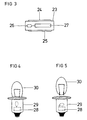
- a circuit arrangement according to the invention is preferably installed in a plate-shaped housing 23 with two contact surfaces 24 and 25, which for example form the terminals 5 and 6 according to FIGS. 1 and 2, in such a way that the circuit arrangement is integrated into an integrated circuit 27 except for a capacitor 26.
- the base of the housing corresponds to the base of the battery type used, such as the base of a mignon, baby and mono cell. The plate is thereby inserted into the battery holder and thus inserted into the circuit between the battery and light bulb.
- a circuit arrangement 28 according to the invention can also be installed in a light bulb base 29, wherein the light bulb base 29 either fixed with an evacuated incandescent lamp bulb ( FIG. 4 ) or serve as a jack for the evacuated bulb 30 ( FIG. 5 ) can.
- the operation of the circuit arrangement according to the invention is based on the fact that it is largely low-current permeable to current. As a result, the light bulb burns with full strength. At regular intervals (for example 1 second), the circuit interrupts the current flow for a short moment (for example in the ms range). During this time, the circuit arrangement over the bulb measures the voltage of the battery (of the accumulator). The measurement itself is high-impedance and is thus hardly distorted by the internal resistance of the incandescent lamp and battery (accumulator). The circuit arrangement according to the invention FIG. 2 remains in the high-resistance state until the measured voltage corresponds at least to the predetermined limit voltage. Thereafter, it turns on again for the predetermined time (eg, 1 second).
- the predetermined time eg, 1 second
- the user is now made aware by short rhythmic dropouts on the approaching "end” of energy reserves. If the lamp is still switched on deliberately, it is possible to achieve a "desired" complete discharge of the accumulator as the dark phases become longer and longer. Thus, on top of that, for example, the unwanted memory effect of NiCd accumulators is prevented.
Landscapes
- Engineering & Computer Science (AREA)
- Power Engineering (AREA)
- Circuit Arrangement For Electric Light Sources In General (AREA)
- Secondary Cells (AREA)
- Protection Of Static Devices (AREA)
Abstract
Claims (12)
- Montage pour protéger une batterie d'une décharge totale, comprenant
deux bornes (5, 6) extérieures, pour le raccordement d'une batterie (1) et d'une charge (3) montée en série avec celle4s-ci,
un interrupteur (9, 15), qui peut être commandé et qui est monté entre les deux bornes (5, 6) extérieures,
un circuit série, qui est monté entre les deux bornes (5, 6) extérieures et en parallèle à l'interrupteur (9, 15), qui peut être commandé et qui est composé d'un accumulateur (8, 14) d'énergie et d'un dispositif (7, 13) de charge de l'accumulateur (8, 14) d'énergie, et
un circuit (11, 16 à 22) de commande, alimenté par l'accumulateur (8, 14) d'énergie et relié à l'interrupteur (9, 15), pour la production d'un signal de commande en fonction d'une valeur limite et de la tension aux bornes de l'interrupteur (9, 15), de façon
à ce que l'interrupteur (9, 15) soit ouvert, pour une tension aux bornes de l'interrupteur (9, 15) ouvert, qui est inférieure à la valeur limite, et, pour une tension aux bornes de l'interrupteur (9, 15) ouvert, qui est supérieure à la valeur limite, soit ouvert pendant des intervalles de temps courts se produisant régulièrement, mais sinon soit fermé. - Montage suivant la revendication 1,
dans lequel le circuit (10, 11, 16 à 22) de commande
a un circuit (10, 16, 17, 18) de contrôle de la tension, pour la production d'un signal de commande en fonction de la valeur limite et de la tension aux bornes de l'interrupteur (9, 15), ainsi qu'
un circuit (11, 14, 16 à 22) de générateur d'impulsions pour la production d'impulsions de courte durée se produisant régulièrement,
le circuit (10, 16, 17, 18) de contrôle de la tension et le circuit (11, 14, 16 à 22) de générateur d'impulsions étant constitués et couplés à l'interrupteur (9, 15) de façon à ce que l'interrupteur (9, 15) soit ouvert, pour une tension aux bornes de l'interrupteur (9, 15) ouvert, qui est inférieure à la valeur limite, et, pour une tension aux bornes de l'interrupteur (9, 15) ouvert, qui est supérieure à la valeur limite, soit ouvert pendant des intervalles de temps courts se produisant régulièrement, mais sinon soit fermé. - Montage suivant la revendication 1 ou 2, dans lequel
il est prévu, comme accumulateur d'énergie, un accumulateur (8) auxiliaire et, comme dispositif de charge, un dispositif (7, 10) de commutation, dans lequel
le dispositif (7, 10) de commutation branche l'accumulateur (8) auxiliaire, pour la charge sur la batterie (1), mais sinon sépare la batterie (1) et l'accumulateur (8) auxiliaire. - Montage suivant la revendication 1 ou 2, dans lequel
il est prévu, comme accumulateur d'énergie, un condensateur (14) et, comme dispositif de charge, une diode (13), dans lequel
la diode (13) est montée de façon à ce que la diode (13) soit passante, lorsque la tension aux bornes de l'interrupteur (9) est plus élevée que la tension aux bornes du condensateur (14), et sinon bloque. - Montage suivant la revendication 4, dans lequel
la tension aux bornes de l'interrupteur (15) est déterminée avec interposition de la diode (13). - Montage suivant la revendication 5, dans lequel le circuit (10, 11, 16 à 22) de commande a
un diviseur (16, 17) de tension, qui est monté en parallèle au condensateur (14) et qui a une prise,
un premier transistor (20) dont la section commandée est montée entre la borne de commande de l'interrupteur (15) et un borne du condensateur (14),
un deuxième transistor (18) dont la section commandée est montée entre la borne de commande du premier transistor (20) et l'autre borne du condensateur (14) et dont la borne de commande est reliée à la prise du diviseur (16, 17) de tension, et
une résistance (22), qui est montée entre la prise du diviseur (16, 17) de tension à la borne de commande de l'interrupteur (15). - Montage suivant l'une des revendications précédentes, dans lequel il est prévu comme interrupteur un troisième transistor (9, 15).
- Montage suivant l'une des revendications précédentes, dans lequel il est prévu comme charge la lampe (29, 30) à incandescence ayant un culot (29) et
qui est intégré dans le culot (29) d'une lampe (29, 30) à incandescence. - Montage suivant l'une des revendications précédentes, qui est incorporé dans un boîtier (23) ayant une surface de base correspond à une surface de base du type de batterie utilisé.
- Montage suivant l'une des revendications précédentes, dans lequel la valeur limite peut être réglée de l'extérieur.
- Montage suivant l'une des revendications 1 à 9,
dans lequel la valeur limite est réglée de manière fixe. - Montage suivant l'une des revendications 1 à 9,
dans lequel il est prévu un dispositif (12), qui règle avec autoapprentissage la valeur limite.
Applications Claiming Priority (1)
| Application Number | Priority Date | Filing Date | Title |
|---|---|---|---|
| PCT/DE2000/001617 WO2001089056A1 (fr) | 2000-05-19 | 2000-05-19 | Circuit pour proteger une batterie de decharges totales |
Publications (2)
| Publication Number | Publication Date |
|---|---|
| EP1310033A1 EP1310033A1 (fr) | 2003-05-14 |
| EP1310033B1 true EP1310033B1 (fr) | 2010-01-06 |
Family
ID=5647684
Family Applications (1)
| Application Number | Title | Priority Date | Filing Date |
|---|---|---|---|
| EP00945538A Expired - Lifetime EP1310033B1 (fr) | 2000-05-19 | 2000-05-19 | Circuit pour proteger une batterie de decharges totales |
Country Status (5)
| Country | Link |
|---|---|
| US (1) | US7006340B2 (fr) |
| EP (1) | EP1310033B1 (fr) |
| JP (1) | JP3706581B2 (fr) |
| DE (1) | DE50015840D1 (fr) |
| WO (1) | WO2001089056A1 (fr) |
Families Citing this family (2)
| Publication number | Priority date | Publication date | Assignee | Title |
|---|---|---|---|---|
| WO2009132850A1 (fr) * | 2008-05-01 | 2009-11-05 | Bayer Bioscience N.V. | Contrôle de la résistance à l’insecte noctuelle à point blanc dans des plantes transgéniques |
| US8274263B2 (en) | 2010-03-30 | 2012-09-25 | Mcpherson Jody | Battery saver |
Family Cites Families (12)
| Publication number | Priority date | Publication date | Assignee | Title |
|---|---|---|---|---|
| US4227191A (en) * | 1978-02-21 | 1980-10-07 | Samuel Raber | Light emitting smoke detector |
| US4342953A (en) * | 1980-05-02 | 1982-08-03 | Nicholl Brothers, Inc. | Battery protection circuit |
| US4423379A (en) * | 1981-03-31 | 1983-12-27 | Sun Electric Corporation | Battery testing techniques |
| US4998888A (en) * | 1984-07-23 | 1991-03-12 | Sgs-Thomson Microelectronics, Inc. | Integrated circuit package with battery housing |
| DE3625905A1 (de) * | 1986-01-14 | 1987-07-23 | Eikoh Giken Co Ltd | Schaltungsanordnung zum pruefen der lebensdauer einer batterie |
| DE3611484C2 (de) * | 1986-04-05 | 1994-06-09 | Ceag Licht & Strom | Schaltungsanordnung für eine tragbare Leuchte |
| US5173653A (en) * | 1988-11-08 | 1992-12-22 | Hochstein Peter A | Battery saver |
| JPH10112939A (ja) * | 1996-10-07 | 1998-04-28 | Nec Corp | 電源切替回路 |
| JP3254159B2 (ja) * | 1997-02-04 | 2002-02-04 | セイコーインスツルメンツ株式会社 | 充放電制御回路 |
| US5966069A (en) * | 1998-03-19 | 1999-10-12 | Prescolite-Moldcast Lighting Company | Exit sign self-testing system |
| US6046574A (en) * | 1999-06-04 | 2000-04-04 | Sony Corporation | Battery dropout correction for battery monitoring in mobile unit |
| US6689512B2 (en) * | 2001-04-11 | 2004-02-10 | Hitachi Maxell Ltd. | Flat-shaped nonaqueous electrolyte battery |
-
2000
- 2000-05-19 JP JP2001585374A patent/JP3706581B2/ja not_active Expired - Fee Related
- 2000-05-19 EP EP00945538A patent/EP1310033B1/fr not_active Expired - Lifetime
- 2000-05-19 DE DE50015840T patent/DE50015840D1/de not_active Expired - Lifetime
- 2000-05-19 WO PCT/DE2000/001617 patent/WO2001089056A1/fr not_active Ceased
-
2002
- 2002-11-19 US US10/299,737 patent/US7006340B2/en not_active Expired - Lifetime
Also Published As
| Publication number | Publication date |
|---|---|
| US7006340B2 (en) | 2006-02-28 |
| JP2003533959A (ja) | 2003-11-11 |
| EP1310033A1 (fr) | 2003-05-14 |
| WO2001089056A1 (fr) | 2001-11-22 |
| DE50015840D1 (de) | 2010-02-25 |
| US20030076073A1 (en) | 2003-04-24 |
| JP3706581B2 (ja) | 2005-10-12 |
Similar Documents
| Publication | Publication Date | Title |
|---|---|---|
| DE69123263T2 (de) | Batterieschutzsystem | |
| DE202017007322U1 (de) | Batterie, Klemme und Ladesystem | |
| DE2440218A1 (de) | Ladegeraet | |
| DE10338082A1 (de) | Anzeigeschaltung für die Batterieladung | |
| EP0115625A1 (fr) | Procédé et dispositif pour indiquer optiquement et/ou acoustiquement l'état de charge d'une batterie ou d'un accumulateur | |
| DE10104594A1 (de) | Schaltung zum Schutz vor tiefer Entladung | |
| DE1438857B2 (de) | Gerät zum Laden von Akkumulatoren | |
| EP1310033B1 (fr) | Circuit pour proteger une batterie de decharges totales | |
| WO2009130061A1 (fr) | Accumulateur d’énergie | |
| DE2559364A1 (de) | Schaltungsanordnung zur automatischen ueberwachung des ladezustandes eines akkumulators | |
| DE3716069A1 (de) | Ladeeinrichtung mit automatischer polungs- und ladespannungswahl, abschaltautomatik und unterspannungs-einschaltschutz fuer wiederaufladbare batterien sowie einfache praezisionsmelde- und schalteinrichtung | |
| DE4116318A1 (de) | Anordnung zum schutz von akkumulatoren gegen tiefentladung | |
| DE2461964B1 (de) | Schaltung zur anzeige des absinkens der spannung einer spannungsquelle | |
| DE3244570C2 (de) | Anordnung zur elektronischen Absicherung batteriebetriebener tragbarer Leuchten | |
| DE19930402B4 (de) | Stromversorgungseinrichtung mit einem Akkumulator zur Speisung eines elektrischen Antriebs eines Lastträgers für Personen | |
| DE3002824C2 (de) | Elektrischer Zünder für Pioniersprengmittel | |
| DE2918960C2 (de) | Schaltungsanordnung zum Prüfen der Betriebsspannung eines batteriebetriebenen Meßgerätes | |
| DE69315709T2 (de) | Schutzvorrichtung zum vermeiden der entladung einer batterie | |
| DE1438857C (de) | Gerat zum Laden von Akkumulatoren | |
| DE3022156A1 (de) | Zeitschalteinrichtung | |
| DE2544548B2 (de) | Schaltungsanordnung zum Laden eines Akkumulators | |
| DE1491881C (de) | Elektrische Signaluhr | |
| DE1638178B2 (de) | Minenzündvorrichtung | |
| EP0389997A2 (fr) | Agencement de circuit pour surmonter les défaillances d'une première source de puissance branchée à un réseau alternatif pour l'alimentation ininterrompue d'interrupteurs horaires électroniques ou électriques, analogiques ou numériques, en particulier horloge commutatrice | |
| DE703922C (de) | Elektrisches Feuerzeug mit Gluehdraht und einer Batterie |
Legal Events
| Date | Code | Title | Description |
|---|---|---|---|
| PUAI | Public reference made under article 153(3) epc to a published international application that has entered the european phase |
Free format text: ORIGINAL CODE: 0009012 |
|
| 17P | Request for examination filed |
Effective date: 20020816 |
|
| AK | Designated contracting states |
Designated state(s): AT BE CH CY DE DK ES FI FR GB GR IE IT LI LU MC NL PT SE |
|
| RBV | Designated contracting states (corrected) |
Designated state(s): AT BE CH DE FR GB LI |
|
| GRAP | Despatch of communication of intention to grant a patent |
Free format text: ORIGINAL CODE: EPIDOSNIGR1 |
|
| RBV | Designated contracting states (corrected) |
Designated state(s): DE FR IT |
|
| GRAS | Grant fee paid |
Free format text: ORIGINAL CODE: EPIDOSNIGR3 |
|
| GRAA | (expected) grant |
Free format text: ORIGINAL CODE: 0009210 |
|
| AK | Designated contracting states |
Kind code of ref document: B1 Designated state(s): DE FR IT |
|
| REF | Corresponds to: |
Ref document number: 50015840 Country of ref document: DE Date of ref document: 20100225 Kind code of ref document: P |
|
| RAP2 | Party data changed (patent owner data changed or rights of a patent transferred) |
Owner name: INFINEON TECHNOLOGIES AG |
|
| PLBE | No opposition filed within time limit |
Free format text: ORIGINAL CODE: 0009261 |
|
| STAA | Information on the status of an ep patent application or granted ep patent |
Free format text: STATUS: NO OPPOSITION FILED WITHIN TIME LIMIT |
|
| 26N | No opposition filed |
Effective date: 20101007 |
|
| REG | Reference to a national code |
Ref country code: FR Ref legal event code: PLFP Year of fee payment: 17 |
|
| PGFP | Annual fee paid to national office [announced via postgrant information from national office to epo] |
Ref country code: IT Payment date: 20160524 Year of fee payment: 17 |
|
| REG | Reference to a national code |
Ref country code: FR Ref legal event code: PLFP Year of fee payment: 18 |
|
| REG | Reference to a national code |
Ref country code: FR Ref legal event code: PLFP Year of fee payment: 19 |
|
| PG25 | Lapsed in a contracting state [announced via postgrant information from national office to epo] |
Ref country code: IT Free format text: LAPSE BECAUSE OF NON-PAYMENT OF DUE FEES Effective date: 20170519 |
|
| PGFP | Annual fee paid to national office [announced via postgrant information from national office to epo] |
Ref country code: FR Payment date: 20180522 Year of fee payment: 19 |
|
| PGFP | Annual fee paid to national office [announced via postgrant information from national office to epo] |
Ref country code: DE Payment date: 20180716 Year of fee payment: 19 |
|
| REG | Reference to a national code |
Ref country code: DE Ref legal event code: R119 Ref document number: 50015840 Country of ref document: DE |
|
| PG25 | Lapsed in a contracting state [announced via postgrant information from national office to epo] |
Ref country code: DE Free format text: LAPSE BECAUSE OF NON-PAYMENT OF DUE FEES Effective date: 20191203 |
|
| PG25 | Lapsed in a contracting state [announced via postgrant information from national office to epo] |
Ref country code: FR Free format text: LAPSE BECAUSE OF NON-PAYMENT OF DUE FEES Effective date: 20190531 |