EP1310955A2 - Circuit d'attaque pour tête d'écriture et méthode d'écriture sur disque de stockage - Google Patents
Circuit d'attaque pour tête d'écriture et méthode d'écriture sur disque de stockage Download PDFInfo
- Publication number
- EP1310955A2 EP1310955A2 EP02257758A EP02257758A EP1310955A2 EP 1310955 A2 EP1310955 A2 EP 1310955A2 EP 02257758 A EP02257758 A EP 02257758A EP 02257758 A EP02257758 A EP 02257758A EP 1310955 A2 EP1310955 A2 EP 1310955A2
- Authority
- EP
- European Patent Office
- Prior art keywords
- current
- head
- terminal
- voltage
- write head
- Prior art date
- Legal status (The legal status is an assumption and is not a legal conclusion. Google has not performed a legal analysis and makes no representation as to the accuracy of the status listed.)
- Withdrawn
Links
Images



Classifications
-
- G—PHYSICS
- G11—INFORMATION STORAGE
- G11B—INFORMATION STORAGE BASED ON RELATIVE MOVEMENT BETWEEN RECORD CARRIER AND TRANSDUCER
- G11B5/00—Recording by magnetisation or demagnetisation of a record carrier; Reproducing by magnetic means; Record carriers therefor
- G11B5/02—Recording, reproducing, or erasing methods; Read, write or erase circuits therefor
- G11B5/022—H-Bridge head driver circuit, the "H" configuration allowing to inverse the current direction in the head
-
- G—PHYSICS
- G11—INFORMATION STORAGE
- G11B—INFORMATION STORAGE BASED ON RELATIVE MOVEMENT BETWEEN RECORD CARRIER AND TRANSDUCER
- G11B5/00—Recording by magnetisation or demagnetisation of a record carrier; Reproducing by magnetic means; Record carriers therefor
- G11B5/012—Recording on, or reproducing or erasing from, magnetic disks
-
- G—PHYSICS
- G11—INFORMATION STORAGE
- G11B—INFORMATION STORAGE BASED ON RELATIVE MOVEMENT BETWEEN RECORD CARRIER AND TRANSDUCER
- G11B5/00—Recording by magnetisation or demagnetisation of a record carrier; Reproducing by magnetic means; Record carriers therefor
- G11B5/02—Recording, reproducing, or erasing methods; Read, write or erase circuits therefor
-
- G—PHYSICS
- G11—INFORMATION STORAGE
- G11B—INFORMATION STORAGE BASED ON RELATIVE MOVEMENT BETWEEN RECORD CARRIER AND TRANSDUCER
- G11B5/00—Recording by magnetisation or demagnetisation of a record carrier; Reproducing by magnetic means; Record carriers therefor
- G11B2005/0002—Special dispositions or recording techniques
- G11B2005/0005—Arrangements, methods or circuits
- G11B2005/001—Controlling recording characteristics of record carriers or transducing characteristics of transducers by means not being part of their structure
- G11B2005/0013—Controlling recording characteristics of record carriers or transducing characteristics of transducers by means not being part of their structure of transducers, e.g. linearisation, equalisation
-
- G—PHYSICS
- G11—INFORMATION STORAGE
- G11B—INFORMATION STORAGE BASED ON RELATIVE MOVEMENT BETWEEN RECORD CARRIER AND TRANSDUCER
- G11B5/00—Recording by magnetisation or demagnetisation of a record carrier; Reproducing by magnetic means; Record carriers therefor
- G11B5/02—Recording, reproducing, or erasing methods; Read, write or erase circuits therefor
- G11B5/09—Digital recording
Definitions
- the present invention relates to circuit and method for writing to a memory disk, and particularly to a circuit and method for differentially driving the write head of a disk drive device.
- disk drives which may be built into or external to the computer system.
- disk drives have at least one rotating magnetic medium and associated head mechanisms that are carried adjacent the magnetic material.
- the heads are radially positionable to selectively write information to, or read information from, precise positions on the disk medium.
- Such disk drives may be, for example, hard disk drives, floppy drives, or the like.
- Data is written to the associated data disk by applying a series of signals to a write head according to the digital information to be stored on the magnetic disk media.
- the write head has a coil and one or more associated pole pieces that are located in close proximity to the disk media.
- signals cause the magnetic flux to change in the head, the magnetic domains of the magnetic media of the disk are aligned in predetermined directions for subsequent read operations.
- a small space of unaligned magnetic media separates each magnetic domain transition to enable successive transitions on the magnetic media to be distinguished from each other.
- the write head assembly includes at least one coil, forcing the current to rise rapidly, or to reverse flux directions within the write head is difficult.
- data writing circuits and/or write drive circuits used to supply such write signals to the heads included preamplifier circuits to drive the current through selected legs of an "H-bridge" circuit, which is capable of allowing relatively fast current reversals for accurate data reproduction.
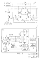
- FIG. 1 An example of a typical H-bridge write head drive circuit 10, according to the prior art, is shown in Figure 1.
- the circuit 10 includes four MOS transistors, 12-15 connected between a high reference voltage V cc and a low reference voltage Vss.
- a coil 19, used, for example, to supply data pulses for writing to a disk drive media is integrated into the write head mechanism.
- the coil 19 is connected between the center legs of the H-bridge, as shown.
- one current flow path includes the transistor 14, coil 19 from right to left, and transistor 13.
- the other current flow path includes transistor 12, the coil 19 from left to right, and the transistor 15.
- the transistor 12 and 14 serve as switching transistors, which are controlled by the out-of-phase signals on a pair of respective input lines 28 and 29.
- the transistors 13 and 15 serve as current controlling transistors, which are controlled by the out-of-phase signals on the respective input lines 29 and 28 in a manner opposite from the connections to the switching transistors 12 and 14, via respective control transistors 31 and 32.
- the magnitude of the current through the transistors 13 and 15 is controlled by a transistor 21, with which the transistors 13 and 15 form respective current mirrors, when connected via respective transmission gates 24 and 25.
- the transmission gates 24 and 25 are controlled by the signals on the respective input lines 29 and 28, in the same manner as the associated transistors 31 and 32.
- a reference current source 26 supplies the reference current to the transistor 21, which is mirrored by currents in respective transistors 13 and 15, as described above.
- the steady state voltage levels to which the two terminals of write head 19 settle are both typically near either the high reference voltage level Vdd or the low reference voltage level Vss.
- wires or lines connecting the write head coil 19 to the write drive circuitry are located proximally to the wires or lines connecting the read head to the read channel circuitry (not shown in Figure 1).
- the close proximity between the wires capacitively couples the wires together.
- voltage spikes or other voltage transitions appearing on the lines connected to write head coil 19 may have a greater tendency to appear as noise on the lines connected to the read head of the disk drive and potentially damage the read head as a result.
- a relatively sizeable voltage spike typically may be generated on a terminal of write head 19 (the terminal of write head 19 having a voltage signal experiencing a falling transition) during the time that the current passing through write head 19 transitions from one direction to another.
- a relatively sizeable voltage spike appears on a terminal of the write head when the write head transitions between steady states.
- this relatively sizeable voltage spike may be capacitively coupled to the lines associated with the read head of the disk drive and thereby damage the read head.
- the rates at which the heads can accurately write the data to the magnetic media is limited by the speed at which the flux in the coil 19 (and its associated components) can be reversed.
- the amplitude of voltage spikes appearing on a write head terminal (and noise appearing on the corresponding read head terminals) is based in part upon the rate of flux reversal.
- the maximum data rate is thus limited to the maximum physical flux reversal rate of the write head drive circuitry and the maximum allowable noise that may be tolerated at the read head during the period of flux reversal.
- Embodiments of the present invention overcome shortcomings in prior write head drive circuitry and satisfy a significant need for a write head circuit and method that effectively drives the write head of a memory disk device so that the write head transitions between steady state conditions relatively rapidly with relatively little noise levels appearing at the read head of the memory disk device.
- Embodiments of the present invention generally provide drive voltage signals to the write head that have no common mode voltage levels during transitions between steady state current levels in the write head. In other words, the drive voltage signals applied to the write head are substantially entirely differential during write head current transitions.
- a driver circuit includes switching circuitry connected between the terminals of the write head and reference voltage supplies, such as positive and negative voltage supplies.
- the driver circuit further includes timing circuitry that generates control signals for controlling the switching circuitry.
- the timing circuitry controls the switching circuitry so that in a first time period, a first terminal of the write head is driven to a first voltage level and a second terminal of the write head is driven to a second voltage level. In a second time period following the first time period, the first terminal is driven to a third voltage level and the second terminal is driven to the fourth voltage level.
- the first, second, third and fourth voltage levels form drive signals for the write head having no common mode voltage.
- the first and fourth voltage levels may be at the level of the negative supply voltage
- the second and third voltage levels may be at the level of the positive supply voltage.
- the third and fourth voltage levels may be approximately zero volts.
- a method of driving a write head includes sourcing a first steady state current level to the first terminal of the head and sinking the first steady state current level from the second terminal of the head.
- the method includes driving, during a first time period, the first terminal of the head to a first voltage level and driving the second terminal to a second voltage level so as to reverse the direction of current flow in the head.
- the first terminal is driven during a second time period to a third voltage level and the second terminal is driven to a fourth voltage level.
- the first, second, third and fourth voltage levels form drive signals for the head having approximately zero common mode voltage.
- a first steady state current level is sunk from the first terminal and the first steady state current level is sourced to the second terminal.
- Disk drive 40 includes a storage medium in the form of one of more disks 41, each of which may contain data on both sides of the disk. Data is written to disks 41 using one or more write heads 42, and read therefrom by one or more read heads 43. Each write head 42 and read head 43 is connected to an arm 44 and is positionally controlled by a voice-coil motor (“VCM”) 45 and a position system 46. The position system 46, through VCM 45, positionally maintains and/or moves write head 42 and read head 43 radially over the desired data on disks 41.
- VCM voice-coil motor
- a read channel 48 converts an analog read signal from read head 43 into digital form.
- a write channel 49 provides data in analog form to write head 42 for storing on a disk 41.
- a pre-amplifier 50 suitably conditions data read from and data to be written to disk 41.
- Channel controller 51 recognizes and organizes the digital data from the read channel 48 and digital data to be sent to write channel 49 into bytes of data.
- An interface adapter 52 provides an interface between channel controller 11 and a system bus 53 that may be particular to the host (data storage, information processing and/or computer) system 1.
- the host system 1 will also typically have other devices that communicate on system bus 53, including a central processing unit (“CPU”) 54 and volatile memory 55.
- CPU central processing unit
- a spindle motor (“SPM”) 56 and SPM control circuit 57 rotate disk 41 and maintain disk 41 at the proper speed for performing a memory access operation (read or write operation).
- the SPM control circuit 57 may communicate with interface adapter 52 or controller 51, as shown in Figure 2. It is understood that disk drive 40 may be divided into and/or include other function blocks from those shown in Figure 2, and that the particular function block implementations illustrated in Figure 2 are presented as an exemplary embodiment of the present invention.
- Driver circuit 100 for driving the write head 42 of a magnetic disk storage device.
- Driver circuit 100 is implemented as an H-bridge circuit wherein current is provided to write head 42 through selected legs of driver circuit 100 for writing data onto an associated magnetic storage disk.
- Driver circuit 100 is located within preamplifier block 50.
- driver circuit 100 applies drive signals to write head 42 so that the amount of time for transitioning current in write head 42 is substantially reduced without introducing noise levels elsewhere in disk drive 42, including noise on read head 43 due to parasitic coupling capacitors that may exist between write head 42 and read head 43.
- the drive signals applied to write head 42 have little if any common mode voltage during current transitions between steady state current levels of the write head current.
- driver circuit 100 includes a plurality of current sources for providing steady state current levels to write head 42.
- a current source 102 is connected between a positive voltage supply Vcc and a first terminal 42a of write head 42, and a current source 104 is connected between first write head terminal 42a and a negative voltage supply Vee.
- current source 106 is connected between positive voltage supply Vcc and a second terminal 42b of write head 42, and a current source 108 is connected between write head terminal 42b and the negative voltage supply Vee.
- Current sources 102 and 108 are connected to write head 42 to source a steady state current to and sink the steady state current from write head 42, respectively, in a first steady state condition.
- current sources 106 and 104 are connected to write head 42 to source a steady state current to and sink the steady state current from write head 42, respectively, in a second steady state condition.
- Current sources 102, 104, 106 and 108 are selectively enabled to source/sink current. When enabled, each current source 102, 104, 106 and 108 allows a current to pass therethrough.
- Figure 3 illustrates each current source 102, 104, 106 and 108 having an enable input connected to a control signal, the generation of which is described below. When the enable signal is asserted (i.e., driven to a voltage corresponding to a logic one), current flows through the current source.
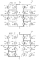
- Figure 4 illustrates a portion of driver circuit 100, and particularly an implementation of current sources 102, 104, 106 and 108 according to an exemplary embodiment of the present invention.
- Current sources 102 and 104 include a primary transistor 140 and control transistors 141 and 142 which are selectively activated to turn primary transistor 140 on and off. Only one control transistor 141, 142 is activated at a time, and one of control transistors 141 and 142 is activated when driver circuit 100 is operating. As a result, the signal driving the gate terminal of transistor 141 is the logical complement of the signal driving the gate terminal of transistor 142. In this case, signal py0 is the logical complement of signal px0, as described below.
- control signal px0 (py0) when control signal px0 (py0) is asserted, reference voltage Vrefp is connected to the gate terminal of primary transistor 140 of current source 102 (106), which turns on primary transistor 140 so as to conduct current.
- control signal px0 (py0) is de-asserted, positive voltage supply Vcc is connected to the gate terminal of primary transistor 140 of current source 102 (106), which turns off primary transistor 140 so that no current flows.
- Current sources 104 and 108 include a primary transistor 150 and control transistors 151 and 152 which are selectively activated to turn primary transistor 150 on and off. Only one control transistor 151, 152 is activated at a time, and one of control transistors 151 and 152 is activated when driver circuit 100 is operating. As a result, the signal driving the gate terminal of transistor 151 is the logical complement of the signal driving the gate terminal of transistor 152. In this case, signal ny0 is the logical complement of signal nx0, as described below.
- control signal nx0 (ny0) when control signal nx0 (ny0) is asserted, reference voltage Vrefn is connected to the gate terminal of primary transistor 150 of current source 104 (108) which turns on primary transistor 150 so as to conduct current.
- negative voltage supply Vee is connected to the gate terminal of primary transistor 150 of current source 104 (108), which turns off primary transistor 150 so that no current flows.
- driver circuit 100 includes switching circuitry which is connected between positive voltage supply Vcc, write head terminals 42a and 42b, and negative voltage supply Vee.
- the switching circuitry may include switching transistors for selectively connecting current sources 102, 104, 106 and 108 to write head 42 (during steady state conditions), and for selectively connecting write head 42 to positive voltage supply Vcc and negative voltage supply Vee (during transitions between steady state conditions).
- the switching circuitry may include first transistor 111 connected in parallel with current source 102, transistor 112 connected in parallel with current source 104, transistor 113 connected in parallel with current source 106 and transistor 114 connected in parallel with current source 108. Further, the switching circuitry may include transistor 116 connected between current source 102 and write head terminal 42a, and transistor 117 connected between current source 104 and write head terminal 42a.
- the phrase "connected in parallel” is used to refer to a transistor having its conduction (drain, source) terminals connected across another component.
- Transistor 118 is connected between current source 106 and write head terminal 42b and transistor 119 is connected between current source 108 and write head terminal 42b.
- the switching circuitry may include transistor 120 connected in parallel with transistor 116, transistor 121 connected in parallel with transistor 117, transistor 122 connected in parallel with transistor 118 and transistor 123 connected in parallel with transistor 119.
- transistors of the switching circuitry are shown in Figure 3 as n-channel transistors, it is understood that the transistors of the switching circuitry may be implemented differently, such as with different types of transistors.
- Driver circuit 100 includes timing circuitry 125 which generates control signals for controlling the conductive state of the transistors of the switching circuitry and current sources 102, 104, 106 and 108.
- Timing circuitry 125 generates a distinct control signal for each transistor of the switching circuitry. In this way, write head 42 may be manipulated so as to relatively rapidly transition between steady state conditions without timing circuitry having to place relatively narrow pulsewidths on the generated control signals.
- timing circuitry 125 includes logic gates or other circuits (not shown) which will provide, at any one time, one or more current paths between positive voltage supply Vcc and write head 42, and between write head 42 and negative voltage supply Vee.
- the specific current paths provided depend upon the particular state of write head 42. Because each transistor of the switching circuitry is independently controlled by timing circuitry 125, the switching circuitry may be relatively easily controlled to generate any of a wide variety of timing-based drive signals to write head 42. The control of the switching circuitry, and particularly the timing of the control signals thereto, to change the direction of current flow in write head 42 is described below.
- Timing circuitry 125 may include programmable or programmed elements, (not shown) to set the desired timing delays for the control signals generated by timing circuitry 125.
- Driver circuit 100 further includes resistive elements 130, 131.
- a resistive element 130, 131 is connected between each write head terminal and a voltage reference, such as the ground reference.
- the single-ended output impedance of driver circuit 100 is approximately equal to the value of resistive elements 130 and 131.
- Each resistive element 130, 131 may have a variable resistance to allow for the single-ended output impedances of driver circuit 100 to be adjusted to match the particular impedances of the lines connecting driver circuit 100 and write head 42.
- driver circuit 100 An operation of driver circuit 100 will be described with reference to Figure 5. The operation described below involves applying drive signals to write head 42 so that current flowing through write head 42 changes from a first steady state to a second steady state. Initially, it is assumed that a steady state current flows through write head 42, from terminal 42a to terminal 42b. In this state, timing circuitry 125 controls the switching circuitry so that steady state current is sourced to terminal 42a from current source 102 (via transistors 116 and 120) and sunk from terminal 42b from current source 108 (via transistors 119 and 123).
- Control signals px0, px2, ny0 and ny2 are driven by timing circuitry 125 to a high logic level to activate (i.e., turn on) transistors 120, 116, 123 and 119, respectively.
- Current sources 104 and 106 are deactivated by timing circuitry 125.
- Transistors 112 and 113 are activated but do not contribute to current sourcing to or sinking from write head 42.
- Transistors 118, 111, 122, 117, 121 and 114 are deactivated.
- the value of resistive elements 130 and 131 serve to set the output voltage levels for write head terminals 42a and 42b.
- Figure 6 shows, in highlighted form, the activated current paths through driver circuit 100 in this steady state condition.
- timing circuitry 125 In the event a write operation is to occur that requires write head 42 to transition to the other steady state condition, timing circuitry 125 enables current paths to write head 42 to cause a current reversal at time T1. Timing circuitry 125 activates current sources 104 and 106 and deactivates current sources 102 and 108. Timing circuitry 125 also activates transistors 113, 122, 121 and 112. Transistors 111, 120, 118, 123, 114 and 117 are turned off. Transistors 116 and 119 are activated but do not serve to source/sink current relative to write head 42. This state causes write head terminal 42b to be connected to positive voltage supply Vcc and write head terminal 42a to be connected to negative voltage supply Vee.
- Timing circuitry 125 maintains the switching circuitry in this state until the current flowing through write head 42 reaches a predetermined overshoot current level that is greater in magnitude than the second steady state current level (i.e., the destination steady state current level).
- Figure 7 shows, in highlighted form, the activated current paths in this first time period during which write head current transitions between the two steady state current levels.
- Timing circuitry 125 drives control signals at time T2 to temporarily reverse the drive signal voltages applied to write head 42.
- timing circuitry 125 drives the control signals to activate transistors 111, 116, 119 and 114.
- Transistors 113, 120, 118, 117, 123 and 112 are turned off.
- Current sources 102 and 108 are turned off.
- Transistors 122 and 121 and current sources 104 and 106 are turned on but do not source/sink current to/from write head 42.
- Resistive elements 130 and 131 may be disconnected from write head terminals 42a and 42b, respectively, in order to prevent current flow.
- write head terminal 42a is connected to positive voltage supply Vcc and write head terminal 42b to be connected to negative voltage supply Vee.
- Vcc positive voltage supply
- write head terminal 42b is connected to negative voltage supply Vee.
- Driver circuit 100 remains in this state for a programmed period of time corresponding to the time it takes for the write head current to reach a predetermined undershoot value that is less in magnitude than the destination steady state current level.
- Figure 8 shows, in highlighted form, the activated current paths in this second time period during which write head current transitions between the two steady state current levels.
- timing circuitry 125 controls the switching circuitry so that write head 42 enters the second steady state condition.
- Timing circuitry 125 drives control signals so that current sources 104 and 106 sink current from and source current to write head 42, respectively. Specifically, timing circuitry activates transistors 118, 122, 121 and 117.
- Transistors 120, 116, 119, 113, 112 and 123 and current sources 102 and 108 are turned off.
- Transistors 111 and 114 are turned on but do not contribute in sourcing/sinking current relative to write head 42.
- a steady state current level is sourced to write head terminal 42b from current source 106 (via transistors 118 and 122) and sunk from write head terminal 42a (via transistors 117 and 121).
- the write head current settles to the steady state current level.
- the values of resistive elements 130 and 131 set the output voltage levels for write head terminals 42a and 42b, respectively.
- Figure 9 shows, in highlighted form, the activated current paths in this steady state condition.
- the write head 42 may be controlled by driver circuit 100 to cause the write head current to transition back to the original steady state current level using timing for the control signals similar to that described above.
- the drive signals applied to write head terminals 42a and 42b are substantially entirely differential, i.e., the drive signals do not possess any common mode signals. Consequently, the capacitive coupling contribution of one drive signal to the read head 43 is substantially entirely offset by the capacitive coupling contribution of the other drive signal to the read head 43, thereby preventing an appreciable amount of noise on the read head 43.
Landscapes
- Digital Magnetic Recording (AREA)
Applications Claiming Priority (2)
| Application Number | Priority Date | Filing Date | Title |
|---|---|---|---|
| US991557 | 2001-11-09 | ||
| US09/991,557 US6970316B2 (en) | 2001-11-09 | 2001-11-09 | Write head driver circuit and method for writing to a memory disk |
Publications (2)
| Publication Number | Publication Date |
|---|---|
| EP1310955A2 true EP1310955A2 (fr) | 2003-05-14 |
| EP1310955A3 EP1310955A3 (fr) | 2007-02-21 |
Family
ID=25537325
Family Applications (1)
| Application Number | Title | Priority Date | Filing Date |
|---|---|---|---|
| EP02257758A Withdrawn EP1310955A3 (fr) | 2001-11-09 | 2002-11-08 | Circuit d'attaque pour tête d'écriture et méthode d'écriture sur disque de stockage |
Country Status (3)
| Country | Link |
|---|---|
| US (1) | US6970316B2 (fr) |
| EP (1) | EP1310955A3 (fr) |
| JP (1) | JP2003187402A (fr) |
Families Citing this family (19)
| Publication number | Priority date | Publication date | Assignee | Title |
|---|---|---|---|---|
| US7099098B2 (en) * | 2003-01-22 | 2006-08-29 | Stmicroelectronics, Inc. | Preamplifier circuit and method for a disk drive device |
| US20050030660A1 (en) * | 2003-08-08 | 2005-02-10 | Ho-Yul Bang | Amplitude spike detector for head instability |
| US7265926B2 (en) * | 2003-10-29 | 2007-09-04 | Texas Instruments Incorporated | High speed hard disk drive with symmetric writer |
| US7113359B2 (en) * | 2003-12-09 | 2006-09-26 | Texas Instruments Incorporated | Impedance-controlled write driver for low power preamp |
| US7375909B2 (en) * | 2004-04-14 | 2008-05-20 | Stmicroelectronics, Inc. | Write driver with power optimization and interconnect impedance matching |
| US7365928B2 (en) * | 2004-04-14 | 2008-04-29 | Stmicroelectronics, Inc. | Write driver with improved boosting circuit and interconnect impedance matching |
| US7035028B2 (en) * | 2004-05-12 | 2006-04-25 | Stmicroelectronics, Inc. | Disk drive write driver with boosting circuit to improve output voltage swing |
| ATE439668T1 (de) | 2004-10-28 | 2009-08-15 | Agere Systems Inc | Verfahren und vorrichtungen zur steuerung des schreibtreiberstroms |
| US7280294B2 (en) * | 2004-11-30 | 2007-10-09 | International Business Machines Corporation | Tri-state servowriter driver with slow return to zero |
| US7701654B2 (en) * | 2005-09-23 | 2010-04-20 | Agere Systems Inc. | Apparatus and method for controlling common mode voltage of a disk drive write head |
| US20070188455A1 (en) * | 2006-02-15 | 2007-08-16 | Logitech Europe S.A. | Single element digital and analog input for a control device |
| US7729077B2 (en) * | 2006-08-30 | 2010-06-01 | Stmicroelectronics, Inc. | Disk drive write driver and associated control logic circuitry |
| US20080204914A1 (en) * | 2007-02-27 | 2008-08-28 | Texas Instruments Incorporated | Low Power Write Driver for a Magnetic Disk Drive |
| JP5084388B2 (ja) * | 2007-07-25 | 2012-11-28 | キヤノン株式会社 | 画像形成装置 |
| US8643969B2 (en) * | 2012-04-26 | 2014-02-04 | Texas Instruments Incorporated | Voltage-mode driver |
| US9105276B2 (en) * | 2013-02-13 | 2015-08-11 | Avago Technologies General Ip (Singapore) Pte. Ltd. | System and method for providing controllable steady state current waveshaping in a hard disk drive (HDD) preamplifier |
| US9978401B1 (en) | 2016-08-19 | 2018-05-22 | Seagate Technology Llc | Chirped current profile with undershoot feature |
| JP2021044704A (ja) * | 2019-09-11 | 2021-03-18 | ローム株式会社 | モータドライバ回路およびハードディスク装置 |
| US20260094615A1 (en) * | 2024-09-30 | 2026-04-02 | Seagate Technology Llc | Write curent undershoot for a heat-assisted magnetic storage device |
Family Cites Families (20)
| Publication number | Priority date | Publication date | Assignee | Title |
|---|---|---|---|---|
| US4551772A (en) * | 1984-03-28 | 1985-11-05 | Storage Technology Corporation | Write drive with current mirrors which reduce feed-through |
| JPH0833974B2 (ja) * | 1987-08-19 | 1996-03-29 | ソニー株式会社 | 磁気ヘッド駆動回路 |
| JPH02285999A (ja) * | 1989-04-26 | 1990-11-26 | Citizen Watch Co Ltd | ステッピングモータの駆動回路 |
| JPH06274805A (ja) * | 1993-03-19 | 1994-09-30 | Hitachi Ltd | リード/ライト集積回路 |
| US5378943A (en) * | 1993-04-20 | 1995-01-03 | International Business Machines Corporation | Low power interface circuit |
| JP3623963B2 (ja) * | 1994-06-10 | 2005-02-23 | コーニンクレッカ フィリップス エレクトロニクス エヌ ヴィ | 情報信号記録装置 |
| US5892371A (en) * | 1996-02-12 | 1999-04-06 | Advanced Micro Devices, Inc. | Gate oxide voltage limiting devices for digital circuits |
| US5751179A (en) * | 1996-04-26 | 1998-05-12 | Crystal Semiconductor | Output driver for PCI bus |
| US6052017A (en) * | 1997-06-30 | 2000-04-18 | Stmicroelectronics, Inc. | Method and circuit for enabling rapid flux reversal in the coil of a write head associated with a computer disk drive, or the like |
| US5926056A (en) * | 1998-01-12 | 1999-07-20 | Lucent Technologies Inc. | Voltage tolerant output buffer |
| US6018257A (en) * | 1998-03-23 | 2000-01-25 | Lsi Logic Corporation | Output drive circuit tolerant of higher voltage signals |
| US6121800A (en) * | 1998-07-07 | 2000-09-19 | Lucent Technologies, Inc. | Impedance matched, voltage-mode H-bridge write drivers |
| US6246533B1 (en) * | 1998-07-13 | 2001-06-12 | Agilent Technologies, Inc. | Programmable write driver circuit for writing information to a magnetic storage media |
| US6054888A (en) * | 1998-10-02 | 2000-04-25 | Advanced Micro Devices, Inc. | Level shifter with protective limit of voltage across terminals of devices within the level shifter |
| US6081152A (en) * | 1998-10-02 | 2000-06-27 | Advanced Micro Devices, Inc. | Output buffer with protective limit of voltage across terminals of devices within the output buffer |
| JP2000268309A (ja) * | 1999-03-19 | 2000-09-29 | Mitsubishi Electric Corp | 書き込み電流駆動回路 |
| US6400190B1 (en) * | 1999-05-07 | 2002-06-04 | Texas Instruments Incorporated | Controlled current undershoot circuit |
| US6236246B1 (en) * | 1999-07-19 | 2001-05-22 | Lucent Technologies Inc. | Voltage-mode boosting circuit for write driver |
| US6252450B1 (en) * | 1999-09-09 | 2001-06-26 | Stmicroelectronics, Inc. | Circuit and method for writing to a memory disk |
| US6504666B1 (en) * | 2000-08-30 | 2003-01-07 | Stmicroelectronics, Inc. | Write head driver circuit and method for writing to a memory disk |
-
2001
- 2001-11-09 US US09/991,557 patent/US6970316B2/en not_active Expired - Lifetime
-
2002
- 2002-11-08 EP EP02257758A patent/EP1310955A3/fr not_active Withdrawn
- 2002-11-11 JP JP2002327083A patent/JP2003187402A/ja active Pending
Also Published As
| Publication number | Publication date |
|---|---|
| US20030090828A1 (en) | 2003-05-15 |
| US6970316B2 (en) | 2005-11-29 |
| JP2003187402A (ja) | 2003-07-04 |
| EP1310955A3 (fr) | 2007-02-21 |
Similar Documents
| Publication | Publication Date | Title |
|---|---|---|
| US6970316B2 (en) | Write head driver circuit and method for writing to a memory disk | |
| US5822141A (en) | High speed FET write driver for an inductive head | |
| US6052017A (en) | Method and circuit for enabling rapid flux reversal in the coil of a write head associated with a computer disk drive, or the like | |
| US6496317B2 (en) | Accurate adjustable current overshoot circuit | |
| EP1083549B1 (fr) | Circuit et méthode pour l'écriture sur un disque de mémoire | |
| US7035028B2 (en) | Disk drive write driver with boosting circuit to improve output voltage swing | |
| US6504666B1 (en) | Write head driver circuit and method for writing to a memory disk | |
| US6512645B1 (en) | Circuit and method for writing to a memory disk with a boosted voltage | |
| US6259305B1 (en) | Method and apparatus to drive the coil of a magnetic write head | |
| US6166869A (en) | Method and circuit for enabling rapid flux reversal in the coil of a write head associated with a computer disk drive, or the like | |
| US6366421B2 (en) | Adjustable writer overshoot for a hard disk drive write head | |
| US6512649B1 (en) | Method for differentially writing to a memory disk | |
| US7035027B2 (en) | Circuits to achieve high data rate writing on thin film transducer | |
| US6400190B1 (en) | Controlled current undershoot circuit | |
| US6275092B1 (en) | Active damping circuit | |
| US7375909B2 (en) | Write driver with power optimization and interconnect impedance matching | |
| US6583946B1 (en) | Method of providing read bias during servo block write | |
| US6975473B2 (en) | Power efficient overshoot protection during an operating mode transition | |
| US6580575B1 (en) | Process and temperature resistant active damping circuit for inductive write drivers | |
| US20030142432A1 (en) | Storage media reading system and semiconductor integrated circuit device | |
| US7099098B2 (en) | Preamplifier circuit and method for a disk drive device | |
| US20010022699A1 (en) | Differentially driven, current mirror based coil driver | |
| JPH11149604A (ja) | コンピュータディスク駆動装置等に関連する書込ヘッドのコイル内の迅速な磁束反転を可能とする方法及び回路 | |
| JPH11149605A (ja) | コンピュータディスクドライブ等に関連する書込ヘッドのコイルにおける迅速な磁束反転を可能とする方法及び回路 | |
| JP4642191B2 (ja) | モータドライバ |
Legal Events
| Date | Code | Title | Description |
|---|---|---|---|
| PUAI | Public reference made under article 153(3) epc to a published international application that has entered the european phase |
Free format text: ORIGINAL CODE: 0009012 |
|
| AK | Designated contracting states |
Designated state(s): AT BE BG CH CY CZ DE DK EE ES FI FR GB GR IE IT LI LU MC NL PT SE SK TR |
|
| AX | Request for extension of the european patent |
Extension state: AL LT LV MK RO SI |
|
| PUAL | Search report despatched |
Free format text: ORIGINAL CODE: 0009013 |
|
| AK | Designated contracting states |
Kind code of ref document: A3 Designated state(s): AT BE BG CH CY CZ DE DK EE ES FI FR GB GR IE IT LI LU MC NL PT SE SK TR |
|
| AX | Request for extension of the european patent |
Extension state: AL LT LV MK RO SI |
|
| 17P | Request for examination filed |
Effective date: 20070808 |
|
| AKX | Designation fees paid |
Designated state(s): DE FR GB IT |
|
| 17Q | First examination report despatched |
Effective date: 20071214 |
|
| STAA | Information on the status of an ep patent application or granted ep patent |
Free format text: STATUS: THE APPLICATION IS DEEMED TO BE WITHDRAWN |
|
| 18D | Application deemed to be withdrawn |
Effective date: 20080625 |