EP1311064A2 - CSD Filterarchitectur mit linearer Phase und mit niederigem Leistungsverbrauch die eine vertikale gemeinsame Unterexpression verwendet und Entwurfsverfahren dafür - Google Patents
CSD Filterarchitectur mit linearer Phase und mit niederigem Leistungsverbrauch die eine vertikale gemeinsame Unterexpression verwendet und Entwurfsverfahren dafür Download PDFInfo
- Publication number
- EP1311064A2 EP1311064A2 EP02253828A EP02253828A EP1311064A2 EP 1311064 A2 EP1311064 A2 EP 1311064A2 EP 02253828 A EP02253828 A EP 02253828A EP 02253828 A EP02253828 A EP 02253828A EP 1311064 A2 EP1311064 A2 EP 1311064A2
- Authority
- EP
- European Patent Office
- Prior art keywords
- vertical common
- csd
- filter
- code words
- subexpression
- Prior art date
- Legal status (The legal status is an assumption and is not a legal conclusion. Google has not performed a legal analysis and makes no representation as to the accuracy of the status listed.)
- Ceased
Links
Images


Classifications
-
- H—ELECTRICITY
- H03—ELECTRONIC CIRCUITRY
- H03H—IMPEDANCE NETWORKS, e.g. RESONANT CIRCUITS; RESONATORS
- H03H17/00—Networks using digital techniques
- H03H17/02—Frequency selective networks
-
- H—ELECTRICITY
- H03—ELECTRONIC CIRCUITRY
- H03H—IMPEDANCE NETWORKS, e.g. RESONANT CIRCUITS; RESONATORS
- H03H17/00—Networks using digital techniques
- H03H17/02—Frequency selective networks
- H03H17/06—Non-recursive filters
-
- H—ELECTRICITY
- H03—ELECTRONIC CIRCUITRY
- H03H—IMPEDANCE NETWORKS, e.g. RESONANT CIRCUITS; RESONATORS
- H03H17/00—Networks using digital techniques
- H03H17/02—Frequency selective networks
- H03H17/0223—Computation saving measures; Accelerating measures
- H03H17/0227—Measures concerning the coefficients
Definitions
- the present invention relates to a digital filter, and more particularly, to low-power CSD (Canonical Signed Digit) linear phase FIR filter architectures using vertical common subexpressions and filter design methods therefor.
- CSD Commercial Signed Digit
- a mobile radio communications system such as a cellular phone requires a low-power and high-speed linear phase Finite Impulse Response (FIR) filter using CMOS techniques.
- FIR Finite Impulse Response
- CMOS complementary metal-oxide-semiconductor
- CSD type coefficients are expressed as binary digits subtracting 1 from 2's complement type coefficients.
- Intermediate frequency (IF) processing terminals of wireless transceivers such as Digital Frequency Down Converter (DFDC) require a high-speed decimation filter. It is preferred that the high-speed/low power filter performs a multiplication using only adders (including subtracter) and delay devices. The high-speed/low power filter can perform the multiplication more efficiently with the CSD type coefficients.
- the numbers b 0, b 1 , b 2 , Across, b N-1 are the CSD type coefficients if each b i 0, +1, -1 and no two consecutive b i are nonzero.
- the CSD type coefficients are expressed by subtracting 2's complement type coefficients from "1". For example, if the 2's complement type coefficient is "01111", the CSD type coefficient can be expressed as "1 - 00001".
- "-1" is expressed as "n” for convenience. That is, when “-1" is expressed as "n”, the 2's complement type coefficient "01111” is expressed as a CSD type coefficient "1000n”. In such a way, all the 2's complement type coefficients are easily converted into CSD type coefficients.
- a filter that performs a multiplication using an adder will require a reduced number of adders in using the CSD type coefficients as filter coefficients.
- the multiplication for filter coefficients is performed using adders and shifts. Because the cost for the filter can be reduced by designing the shift as hardwired logic, it is desirable to reduce the number of adders to reduce the cost for the filter.
- Table 1 lists 4-bit filter coefficients expressed as 2's complement type digits and corresponding CSD type digits. As shown in Table 1, the 2's complement type coefficients have 32 digits "1" and the CSD type coefficients have 23 digits "1". That is, the CSD type coefficients has the number of digits "1" less than in the 2' complement type coefficients by 9 digits "1".
- Table 2 shows CSD type coefficients of a linear phase FIR filter having 11 taps.
- each of the coefficients h 0 , h 1 , h 2 , h 3 , h 4 is symmetric to each of the coefficients h 10 , h 9 , h 8 , h 7 , h 6 , so that the linear phase FIR filter has two common subexpressions.
- An output signal (y) of the FIR filter is expressed by a following formula y [n]: wherein since a ij has digits "1, 0, or -1", the output signal is expressed as the sum of various shifted and delayed versions of input signals (x).
- Each row X ij indicates “delay” of the input signal (x) and each column X ij indicates "shift” of the input signal (x).
- An entry ⁇ 1 in a row i and a column j is represented as ⁇ x 1 [-i]>>j, and a first row (h0) and a first column (2 ⁇ -1) are defined by "x1" without i and j and determined as a reference point.
- (2 ⁇ -2) indicates -2 multiplication of 2 (i.e., 2 -2 ).
- the linear phase FIR filter in Table 2 may be designed using a conventional horizontal common subexpression sharing method to reduce the number of adders. As shown in Table 2, the number of common subexpressions for "n0n", "n001" and "n01" is two.
- the symbol “>>” denotes "shift” of the input signal (x) in a lowest level bit (LSB) direction.
- LSB lowest level bit
- a highest level bit (MSB) out of n0n is "-x 1 "
- the LSB' out of n0n is -x 1 shifted to a right direction by 2 bits, so that "n0n” is expressed as the sum of the results, i.e., "-x 1 -x 1 >> 2”.
- x 2 is defined as a horizontal common subexpression of "n0n”. Similar to the common subexpression for "n0n", the horizontal common subexpression for "n001" is defined as "x 3 ", i.e., "-x 1 +x 1 >> 3".
- the output signal (y) of the filter using the horizontal common subexpression sharing method is expressed by following equation.
- y x 1 >>8 + x 2 [-1]>>6 +x 3 [-2]>>3 +x 4 [-3]>>1 +x 1 [-4]>>1 +x 1 [-5] + x 1 [-6]>>1 + x 4 [-7]>>1 +x 3 [-8]>>3 + x 2 [-9]>>6 +x 1 [-10]>>8
- "x 1 >>8" indicates "1" in a first row (h0) and a ninth column (2 ⁇ -9) in Table 2.
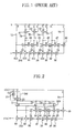
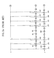
- symbol Ai (“i" is a natural number greater than 1) indicates adders connected to tap lines T1 through T6, symbol Di indicates delayers, x indicates an input signal, and y indicates an output signal.
- Numerals next to the tap lines indicate the number of bits to be shifted.
- the numeral "9" next to the tap line T1 indicates that a digital input signal (x) to be filtered is shifted to a LSB direction by 9 bits.
- Shift registers are employed in the configuration of FIG. 1 to perform a multiplication by shifting the input signals in response to clock signals.
- the adders Ai having a symbol "-" at input terminals thereof perform negative additions, i.e., subtracts. It should be noted that the term "adder” used in this disclosure includes the addition function for performing positive addition as well as the subtraction for performing negative addition.
- the coefficient h0 in Table 2 is implemented on the tap line T1. That is, "x 1 >>8" is implemented using a shift register.
- the horizontal common subexpression x 2 is calculated by the shift registers, each register shifting the input signal (x) by 1 and 3, and the adder A1 connected to the line T2.
- the "x 2 [-1]>> 6" is implemented by the adder A4 that adds up the output (that is shifted by 6 bits) of the shift register connected to the tap line T2 and the output of the delayer D1 (that delays the output of the tap line T1 by one clock cycle).
- the adder A12 implements "x 2 [-9] >> 6”
- the adder A5 implements "x 3 [-2]>>3
- the adder A11 implements "x 3 [-8] >> 3".
- FIG. 1 multiplies the input signal (x) by 9 via the shift register, prior to performing addition operations, so that "-n" in Fig. 1 is implemented by a shift register hardware.
- Each of the delayers D1 through D10 delays the output of the adder inputted to the input terminal thereof by a predetermined time in order to obtain the output signal (y).
- the reason the coefficient h0 is implemented to -1, -4 and -7 is that since x 1 is a reference point shifted by -1, x 1 should be once more shifted by -1 than in the implementing formula when x 1 is implemented.
- MILP mixed integer programming
- a high-speed FIR digital filter structure using minimum numbers of adders is disclosed by M. Yagyu, A. Nishihara and N. Fujii, "Fast FIR digital filter structures using minimal number of adders and its application to filter design", IEICE Transaction on Fundamentals, Vol. E79 A, No. 8, pp. 1120-1129, August 1996.
- the conventional methods reduce the number of adders by searching and sharing common subexpressions in coefficients but symmetric common subexpressions of linear phase filter coefficients.
- the reduced number of adders is not sufficient to implement a high-speed and low-power semiconductor chip.
- the conventional linear phase CSD filter employs only the horizontal common subexpressions, because it is advantage to use common subexpressions naturally generated at both sides thereof due to the symmetric structures of the filters.
- the conventional horizontal common subexpressions sharing method is not adequate to be used in high-speed and low power filters, because the method still requires relatively large numbers of adders.
- a method is provided to implement filter coefficients in a linear phase digital filter in which CSD (Canonical Signed Digit) filter coefficients are used as filter coefficients, and the CSD filter coefficient are expressed with CSD code words in a predetermined number of bits.
- the method comprises the steps of determining vertical common CSD code words between corresponding CSD code words of adjacent filter coefficients, wherein a vertical common CSD code word in a highest level bit is set as a vertical common subexpression, expressing the vertical common CSD code words out of the CSD code words of each filter coefficient with the vertical common subexpression by shifting and delaying the vertical common subexpression, and synthesizing the expressed vertical common CSD code words of the filter coefficients.
- a method is provided to implement a digital filter comprising filter coefficients expressed with CSD (Canonical Signed Digit) code words of n bits (n is a natural number greater than or equal to 2) for filtering digital samples of k bits (k is a natural number greater than or equal to 4).
- the method comprises the steps of generating a vertical common subexpression by searching vertical common CSD code words between corresponding CSD code words of adjacent filter coefficients and determining a vertical common CSD code word in a highest-level bit of the vertical common CSD code words as the vertical common subexpression, and converting the vertical common CSD code words out of each filter coefficient to a shifted and delayed vertical common subexpression such that the filter coefficients are synthetically implemented.
- CSD Physical Signed Digit
- a linear phase digital filter using CSD (Canonical Signed Digit) filter coefficients expressed with CSD code words of a given number of bits as filter coefficients at taps of delay lines comprises a vertical common subexpression generator, connected to a data input terminal, for setting a vertical common CSD code word in a highest level bit of vertical common CSD code words if corresponding CSD code words of adjacent filter coefficients have a plurality of the vertical common CSD code words as a vertical common subexpression, a shift register comprising a plurality of shifters commonly connected to an output terminal of the vertical common subexpression generator, each shifter shifting the output of the vertical common subexpression generator by a predetermined number of bits different from each other, a plurality of adders, each adder being connected to one of the shifters, and a plurality of delayers, each delayer being alternatively connected to an output terminal of corresponding adder of the adders and for delaying the output of the corresponding adder by a unit time.
- CSD Physical Signed Digit
- a linear phase digital filter in which CSD (Canonical Signed Digit) filter coefficients expressed with CSD code words of a predetermined number of bits are used as filter coefficients at taps of delay lines comprises a plurality of vertical common subexpression generators, connected to a plurality of data input terminals respectively, for setting a highest-level bit of vertical common CSD code words of adjacent filter coefficients as vertical common subexpression, respectively, a plurality of shift registers, each shift register being commonly connected to an output terminal of corresponding one of the vertical common subexpression generators and comprising a plurality of output terminals for shifting and outputting an output of the corresponding vertical common subexpression generator by a predetermined number of bits different from each other, a plurality of adders connected to the plurality of output terminals of the shift registers, respectively, and a plurality of delayers alternatively connected to the adders and for delaying the output of the adders by a unit time, respectively.
- CSD Physical Signed Digit
- a shift register commonly connected to an output terminal of the addition member of the vertical common subexpression generator, compris
- filter coefficients according to one aspect of the present invention are implemented using vertical common subexpressions, the number of adders for implementing a digital filter is minimized thereby forming a high-speed and low-power digital filter.
- filter coefficients to be processed are implemented using a vertical common subexpression. It is preferable to use full adders having a plurality input terminals except for where the adders are used in first input terminals of a filter.
- the full adder comprises two half adders and one OR gate.
- the half adder comprises one exclusive OR gate and one AND gate.
- a delayer may be configured with flip-flop or register.
- Table 3 shows filter coefficients grouped in a vertical direction according to the present invention (which is to be contrasted with Table 2 in which the filter coefficients are grouped in a horizontal direction).
- each box in double lines denotes a group of vertical common subexpressions
- each blank denotes a numeral "0”
- each column indicates a 1-bit CSD type filter coefficient
- each row indicates a tap of a filter.
- a tap "h0” has a CSD filter coefficient "000000001”.
- a term "2 ⁇ -1” indicates -1 multiplication of 2 (i.e., 2 -1 )
- a term “2 ⁇ -2” indicates -2 multiplication of 2 (i.e., 2 -2 ).
- a cross point of a first row (h0) and a first column (2 ⁇ -1) is defined as a reference point "x 1 ". If a signal is moved to a horizontal direction from the reference point "x 1 ", the signal is shifted to a lowest level bit direction (LSB). If moved to a vertical direction, the signal is delayed by a unit time.
- LSB lowest level bit direction
- a vertical common subexpression "1n” may be obtained form CSD code words of adjacent filter coefficients.
- the vertical common subexpression "1n” of a tap (h0) filter coefficient and a tap (h1) filter coefficient is obtained from the ninth bits of the CSD code words (000000001) of the tap (h0) and the CSD code words (000000n0n) of the tap (h1).
- the vertical common subexpression "n1" of a tap (h1) filter coefficient and a tap (h2) filter coefficient is obtained from the seventh bits of the CSD code words (000000n0n and 000n00100) of h1 and h2. If the CSD code words of the adjacent filter coefficients have a plurality of vertical common CSD code words, a vertical common CSD code word in a highest level bit (MSB) of the vertical common CSD code words is assigned as the vertical common subexpression.
- MSB highest level bit
- the vertical common subexpression "x 2 " is the sum (in this case, negative sum) of a coefficient (i.e., 1) of the reference point “x 1 " and a coefficient (i.e., n) of the vertically delayed (1tap delayed) and inverted (minus sign or plus sign) reference point “x 1 ". Therefore, if a digit "1" locates at a cross point of a row 1 (h0) and a column 1 (2 ⁇ -1) and a digit "n” locates at a cross point of a row 2 (h1) and a column 1, the vertical common subexpression "x 2 " is defined as a group of these digits in a vertical direction.
- a filter requires one adder (in this case, subtracter) to implement the vertical common subexpression "x 2 ", and an output signal (y) of the filter may be expressed as follow.
- y x 2 >>8 - x 2 [-1]>>6 -x 2 [-2]>>3 -x 2 [-3]>>1 +x 1 [-4] +x 2 [-5]>>1 + x 2 [-6]>>3 + x 2 [-7]>>6 -x 2 [-8]>>8 wherein the symbol ">>” indicates shifting of an input signal (x) and the symbol "[ ]" indicates delaying of the input signal (x).
- the symbol “x 2 >>8” means that the vertical common subexpression “x 2 " is shifted to a right direction by 8 bits
- the symbol “x 2 >>8” indicates “1 and n” located at cross points of rows 1 (h0) and 2 (h1) and a column 9 (2 ⁇ -9).
- the symbol “- x 2 [-1] >> 6” means that the vertical common subexpression “x 2 " is delayed to a vertical direction by 1 (1 tap) and shifted to a right direction by 6 bits.
- the symbol indicates that "n and 1" are located at cross points of rows 2 (h1) and 3 (h2) and column 7 (2 ⁇ -7).
- the output signal of the filter is implemented by synthesizing converted values, i.e., shifted and delayed values of CSD code words of filter coefficients having the vertical common subexpression "x 2 " with reference to the vertical common subexpression "x 2 ".
- a filter requires total 9 adders comprising 8 adders for implementing the output signal (y) according to the above formula, like the filter as shown in FIG. 2, and one adder for implementing the vertical common subexpression "x 2 ".
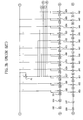
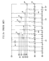
- FIG. 2 shows a linear phase digital filter architecture using a vertical common subexpression method according to an embodiment of the present invention.
- the linear phase digital filter has CSD filter coefficients expressed with CSD code words having a given number of bits as filter coefficients at taps of delay lines.
- the linear phase digital filter comprises a vertical common subexpression generator 100 comprising an adder A1 and a delayer D1 connected to a data input terminal x [n] and for assigning a vertical common subexpression to a highest level bit of the CSD code words when there are a plurality of vertical common subexpressions in the CSD code words of the adjacent filter coefficients, a shift register 200 comprising a plurality of shifters commonly connected to an output terminal of the adder A1 and for shifting the output of the adder A1 by a predetermined number of bits, the shifters being arranged in a highest level shifted bit, i.e., in the order of 8-bit shifter, 6-bit shifter, 3-bit shifter and 1-bit shifter, a plurality of adders A2,A3,A4,A6,A7,A8,A9, each input terminal being connected to each output terminal of the shifters of the shift register 200, and a plurality of delays D3,D4,D8,D9,D10 alternatively connected to the adders and for
- the adders connected to tap lines T1 through T6 are designated as Ai (i is a natural number greater than 1), delayers as Di, an input signal as x, and an output signal as y, respectively.
- the numeral next to the tap lines T2-T5 indicates the number of shifted bits.
- the numeral "8" next to the tap line T2 means that the input signal (x) to be filtered is shifted by 8 bits to a LSB direction. Shift registers may be used for a multiplication in which the input signal (x) is shifted in response to a clock signal.
- a subtracter is not illustrated in FIG. 2, the adders with the symbol "-" at input terminals thereof indicate substracters.
- the vertical common subexpression "x 2 " (i.e., "1n") is implemented at line T2 in FIG. 2. That is, the vertical common subexpression "1n” in Table 3 is implemented with the adder A1 (in this case, subtraction) that adds the coefficient (in this case, 1) of the reference point "x 1 " and the coefficient (in this case, n) of delayed (ltap delayed with the delayer D1) and inverted reference point “x 1 ". Accordingly, the delayer D1 and the adder A1 construct the vertical common subexpression generator 100.
- the vertical common subexpression "x 2 " output from vertical common subexpression generator 100 is shifted by 8 bits through the 8-bit shifter of the shift register 200 and the tap line T2, so that the coefficients h 0 , h 1 and h 9 , h 10 in Table 3 are implemented.
- the tap line T2 is for implementing "x 2 >>8" and "-x 2 [-8]>>8", and the adder A9 is for calculating "-x 2 [-8]>>8".
- the tap line T3 outputs the 6-bit shifted vertical common subexpression x 2 through the 6-bit shifter of the shift register 200 to implement the coefficients h 1 , h 2 and h 8 , h 9 in Table 3.
- the line T3 is for implementing "-x 2 [-1]>>6" and "x 2 [-7]>>6", the adder A2 calculates "-x 2 [-1]>>6" and the adder A8 calculates "x 2 [-7]>>6".
- the line T4 outputs the 3-bits shifted vertical common subexpression x 2 through the 3-bit shifter of the shift register 200 to implement the coefficients h 2 , h 3 and h 7 , h 8 in Table 3.
- the line T4 is for implementing "-x 2 [-2]>>3" and "x 2 [-6]>>3", the adder A3 calculates "-x 2 [-2]>>3” and the adder A7 calculates "x 2 [-6]>>3".
- the coefficients h 3 , h 4 and h 6 , h 7 in Table 3 are implemented through the tap line T5.
- the line T5 is for implementing "-x 2 [-3]>>1" and "x 2 [-5]>>1", the adder A4 calculates "-x 2 [-3]>>1" and the adder A6 calculates "x 2 [-5]>>1".
- the coefficient h 5 is implemented through the tap line T6 for implementing "x 1 [-4]", instead of using the vertical common subexpression.
- the adder A5 computes the x 1 [-4]. Since x 1 is a reference point having 1-bit shift to a lowest level bit direction and requires one more shift to be implemented, a shift bit "1" is required in implementing the coefficient h 5
- the delayers Di delay the outputs of the corresponding adders by a unit time to obtain the output signal (y).
- the delay timing comprises one clock cycle.
- the digital filter according to the present invention comprises the plurality of adders A9,A2,A3,A4,A6,A7,A8 commonly connected to the tap line T2 outputting the vertical common subexpression "x 2 " through the corresponding 8, 6, 3, 1-shifters of the shift register (200).
- the filter architecture of FIG. 2 using the vertical common subexpression method requires the number of adders less than the number of adders in a conventional filter architecture (as shown in FIG. 1) by 4 adders, a reduction ratio of 30.8% in the number of adders is achieved.
- FIG. 7 shows an IF digital signal processor of a wireless receiving terminal employing a digital filter according to the present invention.
- an analog input signal is received through a RF signal processor 10 and is input to an intermediate frequency processor 20 comprising a A/D converter 22, multipliers 24, 25, first and second low pass filters (LPFs) 26, 27, and first and second decimators 28, 29.
- LPFs low pass filters
- the analog signal is converted into digital samples having a predetermined bit by the A/D converter 22 to output to the first and second multipliers 24, 25.
- the multipliers 24, 25 respectively multiply the digital samples by cos ⁇ n and sin ⁇ n to mix them, and provide the mixed signal to the first and second low pass filters (LPFs) 26, 27.
- the first and second low pass filters 26, 27 filter the mixed signal in a given band and output the filtered signal to the corresponding decimators 28, 29.
- the decimators 28, 29 decimate the filtered intermediate frequency signal to generate signals I, Q and provide the signals I, Q to the base band processor 30.
- the base band processor 30 performs channel coding and source coding of the signals I, Q.
- the intermediate frequency processor 20 can be implemented with a Digital Frequency Down Converter (DFDC) as shown in FIG. 8 in which an integrated circuit "HSP50214" of Harris Semiconductor is illustrated.
- the circuit of FIG. 8 comprises a CIC filter 2, a CSD filter 3 and a parallel filter 4 all connected to a mixer 1.
- the CSD filter 3, comprising a half band filter and a programmable filter, may be implemented with the vertical common subexpression method according to the present invention, because the filter 3 necessarily requires a high-speed and low power operation.
- a sampling frequency of a digital filter was 19.6608 MHz
- a pass band frequency and an amount of damping were 630 KHz and 0.1 dB, respectively
- a stop band frequency and an amount of damping were 1.2288 MHz and -40 dB, respectively.
- a linear phase filter was designed using a COSSAP FIR filter design tool according to the specification, so that a linear phase filter coefficient of 73 taps was achieved.
- Table 4 shows CSD type coefficients of 24-bit precision for 37 coefficients except 36 symmetric coefficients out of the above 73 filter coefficients.
- "-1" is indicated as “n”
- columns indicate coefficients of h 0 through h 36 and rows indicates bits of 2 -1 through 2 -24 .
- Table 5 shows conventional horizontal common subexpressions generated with 1 bit to 9 bits out of the CSD coefficients in Table 4
- Table 6 shows vertical common subexpressions generated with 1bit to 9bits out of the CSD coefficients in Table 4.
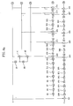
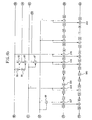
- FIGS. 3A, 3B and 3C show a 9-bit CSD linear phase filters implemented according to the conventional horizontal common subexpression of Table 5.
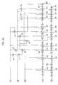
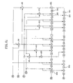
- FIGS 4A and 4B show a configuration of the 9-bit CSD linear phase filter implemented according to the present invention, like the configuration as shown in FIG. 2. Compared with the configurations of FIG. 3, the configuration of FIG. 4 achieves a reduction of 64.5 % in the number of adders.
- Tables 7 and 8 respectively conventional horizontal common subexpressions and vertical common subexpressions of the present invention generated with 1 bit to 10 bits out of the CSD coefficients in Table 4.
- FIGS. 6A, 6B and 6C show configurations of a 10-bit CSD linear phase filter implemented with the vertical common subexpressions in Table 8.
- FIGS. 5A and 5B show configurations of a 10-bit CSD linear phase filter implemented with the horizontal common subexpressions in Table 7.
- the filter of FIG. 5 requires 74 adders, while the filter of FIG. 6 requires 49 adders.
- the vertical common subexpression method of present invention accomplishes a reduction of 33.8 % in the number of adders.
- Table 9 shows the number of adders for implementing 9bits to 16bits in Table 4 when coefficients of the bits is respectively implemented with a conventional horizontal common subexpression method and a vertical common subexpression method of the present invention. As shown in Table 9, the number of adders implemented with the vertical common subexpression method is less than the number of adders implemented with the horizontal common subexpression method.
- the vertical common subexpression method according to the present invention can achieve higher efficiency in implementing the less number of bits.
- a specification of a CDMA IS-95 intermediate frequency terminal (that is suggested by Qualcomm) was implemented with a vertical common subexpression method of the present invention.
- a sampling frequency of a digital filter was 19.6608 MHz
- a pass band frequency and an amount of damping were 630 KHz and 0.1 dB
- a stop band frequency and an amount of damping were 820 MHz and -40 dB, respectively.
- a filter was designed using the MATLAB FIR filter design tool to meet the specification, so that the linear phase filter coefficients of 219 taps were achieved. 110 coefficients except 109 symmetric coefficients out of the total 219 filter coefficients were converted into 2's complement type of 20 bits and thereafter were represented with CSD type coefficients.
- Table 10 respectively shows the number of adders for implementing 9bits to 16bits in Table 4 when coefficients of the bits is respectively implemented with a conventional horizontal common subexpression method and a vertical common subexpression method of the present invention. As shown in Table 10, the reduction ratio in the number of adders is greater when the number of bits is smaller. Reduction ratio in the number of additions of vertical common subexpression relative to a conventional method (219 taps) Conventional horizontal common subexpression Vertical common subexpression Saving (%) 9bit 108 56 48.15 10bit 153 80 47.71 11 bit 203 116 44.76 12bit 223 136 39.01 13bit 226 172 27.12 14bit 248 193 22.18 15bit 270 227 15.93 16bit 288 244 15.28
- the average reduction ratio in the number of adders of the vertical common subexpression method of the present invention relative to the conventional horizontal common subexpression method was 22.11 %.
- the performance of the vertical common subexpression method of the present invention was higher at a higher order filter (that is, the filter having 219taps) than a lower order filter (that is, the filter having 73taps).
- the vertical common subexpression method according to the present invention may be employed in a general filter as well as in a linear phase FIR filter.
Landscapes
- Engineering & Computer Science (AREA)
- Physics & Mathematics (AREA)
- Computer Hardware Design (AREA)
- Mathematical Physics (AREA)
- Computing Systems (AREA)
- Theoretical Computer Science (AREA)
- Complex Calculations (AREA)
- Digital Transmission Methods That Use Modulated Carrier Waves (AREA)
- Filters That Use Time-Delay Elements (AREA)
- Compression, Expansion, Code Conversion, And Decoders (AREA)
Applications Claiming Priority (2)
| Application Number | Priority Date | Filing Date | Title |
|---|---|---|---|
| KR10-2001-0070065A KR100422449B1 (ko) | 2001-11-12 | 2001-11-12 | 수직 공통패턴을 사용한 저전력 csd 선형위상 디지털필터 구조 및 그에 따른 필터구현방법 |
| KR2001070065 | 2001-11-12 |
Publications (2)
| Publication Number | Publication Date |
|---|---|
| EP1311064A2 true EP1311064A2 (de) | 2003-05-14 |
| EP1311064A3 EP1311064A3 (de) | 2005-04-27 |
Family
ID=19715899
Family Applications (1)
| Application Number | Title | Priority Date | Filing Date |
|---|---|---|---|
| EP02253828A Ceased EP1311064A3 (de) | 2001-11-12 | 2002-05-30 | CSD Filterarchitectur mit linearer Phase und mit niederigem Leistungsverbrauch die eine vertikale gemeinsame Unterexpression verwendet und Entwurfsverfahren dafür |
Country Status (5)
| Country | Link |
|---|---|
| US (1) | US7016926B2 (de) |
| EP (1) | EP1311064A3 (de) |
| JP (1) | JP2003188685A (de) |
| KR (1) | KR100422449B1 (de) |
| CN (1) | CN100391280C (de) |
Families Citing this family (13)
| Publication number | Priority date | Publication date | Assignee | Title |
|---|---|---|---|---|
| US7529788B2 (en) * | 2002-10-21 | 2009-05-05 | Neuro Solution Corp. | Digital filter design method and device, digital filter design program, and digital filter |
| US20050171988A1 (en) * | 2002-10-21 | 2005-08-04 | Neuro Solution Corp. | Digital filter design method and device, digital filter design program, and digital filter |
| KR100644271B1 (ko) * | 2004-07-16 | 2006-11-10 | 한국전자통신연구원 | 군지연 등화된 다중 통과 대역 필터 구현 방법 |
| US20060020650A1 (en) * | 2004-07-20 | 2006-01-26 | Guozhong Shen | Ripple elimination filter |
| EP1650869A1 (de) * | 2004-10-20 | 2006-04-26 | STMicroelectronics Pvt. Ltd | Eine Vorrichtung zur Implementierung eines Summenprodukt-Ausdrucks |
| US20060218213A1 (en) * | 2005-03-24 | 2006-09-28 | Shereef Shehata | Optimization technique for FIR and IIR filter design |
| WO2007013036A2 (en) * | 2005-07-29 | 2007-02-01 | Nxp B.V. | Digital filter |
| US9106394B1 (en) * | 2006-02-24 | 2015-08-11 | The United States of America as presented by the Secretary of the Navy | Signal event detection system |
| US8819095B2 (en) * | 2007-08-28 | 2014-08-26 | Qualcomm Incorporated | Fast computation of products by dyadic fractions with sign-symmetric rounding errors |
| CN102170276B (zh) * | 2011-03-01 | 2013-08-21 | 深圳市蓝韵实业有限公司 | 一种用于超声信号处理的升采样滤波方法 |
| KR20160057590A (ko) | 2014-11-13 | 2016-05-24 | 삼성디스플레이 주식회사 | 공통 부분식 소거 방법 및 이를 이용한 필터 |
| CN110830005B (zh) * | 2019-11-13 | 2023-01-24 | 中国科学院微电子研究所 | 数字滤波器电路的实现方法及系统 |
| CN116149600B (zh) * | 2023-03-13 | 2023-09-08 | 深圳鸿芯微纳技术有限公司 | 多常数乘法器的逻辑电路设置方法、装置、设备及介质 |
Family Cites Families (7)
| Publication number | Priority date | Publication date | Assignee | Title |
|---|---|---|---|---|
| US5058047A (en) * | 1989-05-30 | 1991-10-15 | Advanced Micro Devices, Inc. | System and method for providing digital filter coefficients |
| KR100248021B1 (ko) * | 1995-09-30 | 2000-03-15 | 윤종용 | Csd 필터의 신호처리방법과 그 회로 |
| US6112218A (en) * | 1998-03-30 | 2000-08-29 | Texas Instruments Incorporated | Digital filter with efficient quantization circuitry |
| US6163788A (en) * | 1998-06-25 | 2000-12-19 | Industrial Technology Research Institute | Programmable finite impulse response processor with scalable dynamic data range |
| US6757326B1 (en) * | 1998-12-28 | 2004-06-29 | Motorola, Inc. | Method and apparatus for implementing wavelet filters in a digital system |
| US6590931B1 (en) * | 1999-12-09 | 2003-07-08 | Koninklijke Philips Electronics N.V. | Reconfigurable FIR filter using CSD coefficient representation |
| KR100422443B1 (ko) * | 2001-02-13 | 2004-03-11 | 삼성전자주식회사 | 버츄얼 공통패턴을 사용한 저전력 csd 선형위상 fir필터 구조 및 그에 따른 필터구현방법 |
-
2001
- 2001-11-12 KR KR10-2001-0070065A patent/KR100422449B1/ko not_active Expired - Fee Related
-
2002
- 2002-05-07 US US10/140,591 patent/US7016926B2/en not_active Expired - Lifetime
- 2002-05-30 EP EP02253828A patent/EP1311064A3/de not_active Ceased
- 2002-06-26 CN CNB021231737A patent/CN100391280C/zh not_active Expired - Lifetime
- 2002-09-26 JP JP2002281050A patent/JP2003188685A/ja active Pending
Non-Patent Citations (4)
| Title |
|---|
| HARTLEY R I: "SUBEXPRESSION SHARING IN FILTERS USING CANONIC SIGNED DIGIT MULTIPLIERS" IEEE TRANSACTIONS ON CIRCUITS AND SYSTEMS II: ANALOG AND DIGITAL SIGNAL PROCESSING, IEEE INC. NEW YORK, US, vol. 43, no. 10, October 1996 (1996-10), pages 677-688, XP000641991 ISSN: 1057-7130 * |
| MEHENDALE M ET AL: "Synthesis of multiplier-less FIR filters with minimum number of additions" 1995 IEEE/ACM INTERNATIONAL CONFERENCE ON COMPUTER-AIDED DESIGN (ICCAD). SAN JOSE, NOV. 5 - 9, 1995, IEEE/ACM INTERNATIONAL CONFERENCE ON COMPUTER-AIDED DESIGN, LOS ALAMITOS, IEEE COMP. SOC. PRESS, US, 5 November 1995 (1995-11-05), pages 668-671, XP010153129 ISBN: 0-8186-7213-7 * |
| POTKONJAK M ET AL: "MULTIPLE CONSTANT MULTIPLICATIONS: EFFICIENT AND VERSATILE FRAMEWORK AND ALGORITHMS FOR EXPLORING COMMON SUBEXPRESSION ELIMINATION" IEEE TRANSACTIONS ON COMPUTER AIDED DESIGN OF INTEGRATED CIRCUITS AND SYSTEMS, IEEE INC. NEW YORK, US, vol. 15, no. 2, 1 February 1996 (1996-02-01), pages 151-165, XP000590734 ISSN: 0278-0070 * |
| YAGYU M ET AL: "FAST FIR DIGITAL FILTER STRUCTURES USING MINIMAL NUMBER OF ADDERS AND ITS APPLICATION TO FILTER DESIGN" IEICE TRANSACTIONS ON FUNDAMENTALS OF ELECTRONICS, COMMUNICATIONS AND COMPUTER SCIENCES, INSTITUTE OF ELECTRONICS INFORMATION AND COMM. ENG. TOKYO, JP, vol. E79-A, no. 8, August 1996 (1996-08), pages 1120-1129, XP000633525 ISSN: 0916-8508 * |
Also Published As
| Publication number | Publication date |
|---|---|
| US20030105787A1 (en) | 2003-06-05 |
| US7016926B2 (en) | 2006-03-21 |
| KR100422449B1 (ko) | 2004-03-11 |
| CN1419388A (zh) | 2003-05-21 |
| KR20030039124A (ko) | 2003-05-17 |
| JP2003188685A (ja) | 2003-07-04 |
| EP1311064A3 (de) | 2005-04-27 |
| CN100391280C (zh) | 2008-05-28 |
Similar Documents
| Publication | Publication Date | Title |
|---|---|---|
| Mahesh et al. | A new common subexpression elimination algorithm for realizing low-complexity higher order digital filters | |
| EP1311064A2 (de) | CSD Filterarchitectur mit linearer Phase und mit niederigem Leistungsverbrauch die eine vertikale gemeinsame Unterexpression verwendet und Entwurfsverfahren dafür | |
| Mahesh et al. | New reconfigurable architectures for implementing FIR filters with low complexity | |
| Chen et al. | A low-power digit-based reconfigurable FIR filter | |
| US8417750B2 (en) | Filters for communication systems | |
| US7277479B2 (en) | Reconfigurable fir filter | |
| JP4665099B2 (ja) | デジタル・フィルタのフィルタ係数を決定する方法およびデジタル・フィルタ | |
| US5784419A (en) | Efficient digital filter and method using coefficient precombing | |
| KR100422443B1 (ko) | 버츄얼 공통패턴을 사용한 저전력 csd 선형위상 fir필터 구조 및 그에 따른 필터구현방법 | |
| US7028062B2 (en) | FIR filter, method of operating the same, semiconductor integrated circuit including FIR filter, and communication system for transmitting data filtered by FIR filter | |
| Zhu et al. | ASIC implementation architecture for pulse shaping FIR filters in 3G mobile communications | |
| Mathew et al. | Realization of low power high-speed channel filters with stringent adjacent channel attenuation specifications for software radio receivers | |
| Smitha et al. | A reconfigurable high-speed rns-fir channel filter for multi-standard software radio receivers | |
| Vinod et al. | Optimizing vertical common subexpression elimination using coefficient partitioning for designing low complexity software radio channelizers | |
| KR100746856B1 (ko) | 무승산기 fir 디지털 필터 및 그 설계 방법 | |
| Mahesh et al. | An architecture for integrating low complexity and reconfigurability for channel filters in software defined radio receivers | |
| Vinod et al. | Complexity reduction of software defined radio channelizers using filter coefficient-partitioning. | |
| Uusikartano et al. | A low-power fractional decimator architecture for an IF-sampling dual-mode receiver | |
| Uusikartano et al. | Power-efficient CIC decimator architecture for f/sub s//4-downconverting digital receivers | |
| Grati et al. | Design and implementation of cascade decimation filter for radio communications | |
| KR20070073462A (ko) | 디지털 통신 시스템에서의 보간 장치 및 방법 | |
| Grati et al. | Design and hardware implementation of digital channel selection processor for radio receiver | |
| Smitha et al. | Low power realization and synthesis of higher-order FIR filters using an improved common subexpression elimination method | |
| Mathew et al. | Realization of low power high-speed channel filters with stringent adjacent channel attenuation specifications for wireless communication receivers | |
| Shahare et al. | A review: FPGA implementation of reconfigurable digital FIR filter |
Legal Events
| Date | Code | Title | Description |
|---|---|---|---|
| PUAI | Public reference made under article 153(3) epc to a published international application that has entered the european phase |
Free format text: ORIGINAL CODE: 0009012 |
|
| 17P | Request for examination filed |
Effective date: 20020613 |
|
| AK | Designated contracting states |
Designated state(s): AT BE CH CY DE DK ES FI FR GB GR IE IT LI LU MC NL PT SE TR |
|
| AX | Request for extension of the european patent |
Extension state: AL LT LV MK RO SI |
|
| PUAL | Search report despatched |
Free format text: ORIGINAL CODE: 0009013 |
|
| AK | Designated contracting states |
Kind code of ref document: A3 Designated state(s): AT BE CH CY DE DK ES FI FR GB GR IE IT LI LU MC NL PT SE TR |
|
| AX | Request for extension of the european patent |
Extension state: AL LT LV MK RO SI |
|
| AKX | Designation fees paid |
Designated state(s): FI GB NL |
|
| REG | Reference to a national code |
Ref country code: DE Ref legal event code: 8566 |
|
| STAA | Information on the status of an ep patent application or granted ep patent |
Free format text: STATUS: THE APPLICATION HAS BEEN REFUSED |
|
| 18R | Application refused |
Effective date: 20091215 |