EP1314255B1 - Verbesserte verfahren und vorrichtung zur auf- und abwärtsumsetzung von hochfrequenzsignalen (rf) - Google Patents
Verbesserte verfahren und vorrichtung zur auf- und abwärtsumsetzung von hochfrequenzsignalen (rf) Download PDFInfo
- Publication number
- EP1314255B1 EP1314255B1 EP01944827A EP01944827A EP1314255B1 EP 1314255 B1 EP1314255 B1 EP 1314255B1 EP 01944827 A EP01944827 A EP 01944827A EP 01944827 A EP01944827 A EP 01944827A EP 1314255 B1 EP1314255 B1 EP 1314255B1
- Authority
- EP
- European Patent Office
- Prior art keywords
- signal
- power
- frequency
- synthesizer
- time
- Prior art date
- Legal status (The legal status is an assumption and is not a legal conclusion. Google has not performed a legal analysis and makes no representation as to the accuracy of the status listed.)
- Expired - Lifetime
Links
- 238000000034 method Methods 0.000 title claims abstract description 34
- 238000006243 chemical reaction Methods 0.000 title abstract description 31
- 238000002156 mixing Methods 0.000 claims abstract description 46
- 239000003990 capacitor Substances 0.000 claims description 6
- 238000012937 correction Methods 0.000 claims description 4
- 230000008878 coupling Effects 0.000 claims description 4
- 238000010168 coupling process Methods 0.000 claims description 4
- 238000005859 coupling reaction Methods 0.000 claims description 4
- 238000001914 filtration Methods 0.000 claims description 4
- 230000003044 adaptive effect Effects 0.000 claims description 3
- 230000000295 complement effect Effects 0.000 abstract description 9
- 239000000047 product Substances 0.000 description 21
- 238000004891 communication Methods 0.000 description 20
- 238000013461 design Methods 0.000 description 13
- 238000010586 diagram Methods 0.000 description 13
- 238000001228 spectrum Methods 0.000 description 13
- 230000006870 function Effects 0.000 description 12
- 230000010354 integration Effects 0.000 description 11
- 230000015654 memory Effects 0.000 description 10
- 230000008569 process Effects 0.000 description 9
- 230000003247 decreasing effect Effects 0.000 description 7
- 230000000737 periodic effect Effects 0.000 description 7
- 230000008901 benefit Effects 0.000 description 6
- 238000004519 manufacturing process Methods 0.000 description 6
- 230000001413 cellular effect Effects 0.000 description 5
- 238000005070 sampling Methods 0.000 description 5
- 230000010363 phase shift Effects 0.000 description 4
- 230000009467 reduction Effects 0.000 description 4
- 238000013519 translation Methods 0.000 description 4
- 230000005540 biological transmission Effects 0.000 description 3
- 230000000694 effects Effects 0.000 description 3
- 238000005516 engineering process Methods 0.000 description 3
- PCHJSUWPFVWCPO-UHFFFAOYSA-N gold Chemical compound [Au] PCHJSUWPFVWCPO-UHFFFAOYSA-N 0.000 description 3
- 239000010931 gold Substances 0.000 description 3
- 229910052737 gold Inorganic materials 0.000 description 3
- 238000002955 isolation Methods 0.000 description 3
- 230000011664 signaling Effects 0.000 description 3
- 238000003892 spreading Methods 0.000 description 3
- 238000003491 array Methods 0.000 description 2
- 230000001419 dependent effect Effects 0.000 description 2
- 230000009977 dual effect Effects 0.000 description 2
- 230000001788 irregular Effects 0.000 description 2
- 230000000670 limiting effect Effects 0.000 description 2
- 239000011159 matrix material Substances 0.000 description 2
- 239000013307 optical fiber Substances 0.000 description 2
- 230000002829 reductive effect Effects 0.000 description 2
- 230000007480 spreading Effects 0.000 description 2
- IRLPACMLTUPBCL-KQYNXXCUSA-N 5'-adenylyl sulfate Chemical compound C1=NC=2C(N)=NC=NC=2N1[C@@H]1O[C@H](COP(O)(=O)OS(O)(=O)=O)[C@@H](O)[C@H]1O IRLPACMLTUPBCL-KQYNXXCUSA-N 0.000 description 1
- 102100032919 Chromobox protein homolog 1 Human genes 0.000 description 1
- 101000797584 Homo sapiens Chromobox protein homolog 1 Proteins 0.000 description 1
- 230000002860 competitive effect Effects 0.000 description 1
- 238000010276 construction Methods 0.000 description 1
- 238000007796 conventional method Methods 0.000 description 1
- 230000007547 defect Effects 0.000 description 1
- 230000001934 delay Effects 0.000 description 1
- 238000000586 desensitisation Methods 0.000 description 1
- 238000011161 development Methods 0.000 description 1
- 238000009826 distribution Methods 0.000 description 1
- 239000000835 fiber Substances 0.000 description 1
- 239000012467 final product Substances 0.000 description 1
- 230000007274 generation of a signal involved in cell-cell signaling Effects 0.000 description 1
- 238000003384 imaging method Methods 0.000 description 1
- 230000007774 longterm Effects 0.000 description 1
- 239000000463 material Substances 0.000 description 1
- 230000007246 mechanism Effects 0.000 description 1
- 238000012986 modification Methods 0.000 description 1
- 230000004048 modification Effects 0.000 description 1
- 238000012544 monitoring process Methods 0.000 description 1
- 238000004806 packaging method and process Methods 0.000 description 1
- 238000011045 prefiltration Methods 0.000 description 1
- 230000004044 response Effects 0.000 description 1
- 230000000717 retained effect Effects 0.000 description 1
- 238000010079 rubber tapping Methods 0.000 description 1
- 238000007493 shaping process Methods 0.000 description 1
- 230000035939 shock Effects 0.000 description 1
- 230000008054 signal transmission Effects 0.000 description 1
- 238000004088 simulation Methods 0.000 description 1
- 239000007787 solid Substances 0.000 description 1
- 238000003860 storage Methods 0.000 description 1
- 239000000758 substrate Substances 0.000 description 1
- 230000001629 suppression Effects 0.000 description 1
- 238000012360 testing method Methods 0.000 description 1
- 238000012876 topography Methods 0.000 description 1
- 238000012549 training Methods 0.000 description 1
- 238000005303 weighing Methods 0.000 description 1
Images




Classifications
-
- H—ELECTRICITY
- H04—ELECTRIC COMMUNICATION TECHNIQUE
- H04B—TRANSMISSION
- H04B1/00—Details of transmission systems, not covered by a single one of groups H04B3/00 - H04B13/00; Details of transmission systems not characterised by the medium used for transmission
- H04B1/02—Transmitters
- H04B1/04—Circuits
- H04B1/0475—Circuits with means for limiting noise, interference or distortion
-
- H—ELECTRICITY
- H03—ELECTRONIC CIRCUITRY
- H03D—DEMODULATION OR TRANSFERENCE OF MODULATION FROM ONE CARRIER TO ANOTHER
- H03D7/00—Transference of modulation from one carrier to another, e.g. frequency-changing
- H03D7/16—Multiple-frequency-changing
- H03D7/161—Multiple-frequency-changing all the frequency changers being connected in cascade
-
- H—ELECTRICITY
- H04—ELECTRIC COMMUNICATION TECHNIQUE
- H04B—TRANSMISSION
- H04B1/00—Details of transmission systems, not covered by a single one of groups H04B3/00 - H04B13/00; Details of transmission systems not characterised by the medium used for transmission
- H04B1/06—Receivers
- H04B1/10—Means associated with receiver for limiting or suppressing noise or interference
- H04B1/1027—Means associated with receiver for limiting or suppressing noise or interference assessing signal quality or detecting noise/interference for the received signal
- H04B1/1036—Means associated with receiver for limiting or suppressing noise or interference assessing signal quality or detecting noise/interference for the received signal with automatic suppression of narrow band noise or interference, e.g. by using tuneable notch filters
-
- H—ELECTRICITY
- H04—ELECTRIC COMMUNICATION TECHNIQUE
- H04B—TRANSMISSION
- H04B1/00—Details of transmission systems, not covered by a single one of groups H04B3/00 - H04B13/00; Details of transmission systems not characterised by the medium used for transmission
- H04B1/06—Receivers
- H04B1/16—Circuits
- H04B1/30—Circuits for homodyne or synchrodyne receivers
Definitions
- the present invention relates generally to communications, and more specifically, to a fully-integrable method and apparatus for up- and down-conversion of radio frequency (RF) and baseband signals with improved performance.
- RF radio frequency
- the original (or baseband) signal may be, for example: data, voice or video.
- These baseband signals may be produced by transducers such as microphones or video cameras, be computer generated, or transferred from an electronic storage device.
- the high frequencies provide longer range and higher capacity channels than baseband signals, and because high frequency RF signals can propagate through the air, they can be used for wireless transmissions as well as hard wired or fibre channels.
- radio frequency signals are electromagnetic signals; that is, waveforms with electrical and magnetic properties within the electromagnetic spectrum normally associated with radio wave propagation.
- the electromagnetic spectrum was traditionally divided into 26 alphabetically designated bands, however, the International Telecommunication Union (ITU) formally recognizes 12 bands, from 30 Hz to 3000 GHz. New bands, from 3 THz to 3000 THz, are under active consideration for recognition.
- ITU International Telecommunication Union
- Wired communication systems which employ such modulation and demodulation techniques include computer communication systems such as local area networks (LANs), point to point signalling, and wide area networks (WANs) such as the Internet. These networks generally communication data signals over electrically conductive or optical fibre channels.
- Wireless communication systems which may employ modulation and demodulation include those for public broadcasting such as AM and FM radio, and UHF and VHF television.
- Private communication systems may include cellular telephone networks, personal paging devices, HF (high frequency) radio systems used by taxi services, microwave backbone networks, interconnected appliances under the Bluetooth standard, and satellite communications. Other wired and wireless systems which use RF modulation and demodulation would be known to those skilled in the art.
- the super-heterodyne receiver uses a two-step frequency translation method to convert an RF signal to a baseband signal.
- Figure 1 presents a block diagram of a typical super-heterodyne receiver 10.
- the mixers labelled M1 12 , MI 14, and MQ 16 are used to translate an incoming RF signal to baseband or to some other frequency. The balance of the components amplify the signal being processed and filter noise from it.
- the RF band pass filter (BPF1) 18 first filters the incoming signal and corruptive noise coming from the antenna 20, attenuating out of band signals and passing the desired signal (note that this band pass filter 18 may also be a duplexer.
- a duplexer is an electronic switch which permits a receiver and transmitter to use the same antenna by alternately interconnecting them with the antenna).
- a low noise amplifier (LNA) 22 then amplifies the filtered antenna signal, increasing the strength of the RF signal and reducing the noise figure of the receiver 10.
- the signal is next filtered by another band pass filter (BPF2) 24 usually identified as an image rejection filter.
- BPF2 band pass filter
- the desired signal, plus residual unwanted signals, then enter mixer M1 12 which multiplies this signal with a periodic sinusoidal signal generated by the local oscillator (LO1) 26.
- the mixer M1 12 receives the signal from the image rejection filter 24 and causes both a down-conversion and an up-conversion in the frequency domain. Usually, the down-converted portion is retained at the
- a mixer is a circuit or device that accepts as its input two different frequencies and presents at its output:
- the frequency conversion process causes a second band of frequencies to be superimposed upon the desired signal at the IF frequency. These "image frequencies" cannot be blocked by a band pass filter 24 so they corrupt the desired signal.
- the typical embodiment of a mixer is a digital switch, which may generate significantly more tones than those described in (a) through (c).
- the IF signal is next filtered by a band pass filter (BPF3) 28 typically called the channel filter, which is centred around the IF frequency, thus filtering out mixer signals (a) and (c) above.
- BPF3 band pass filter
- the signal is then amplified by an amplifier (IFA) 30, and is split into its in-phase (I) and quadrature (Q) components, using mixers MI 14 and MQ 16 and orthogonal mixing signals generated by local oscillator (LO2) 32 and 90 degree phase shifter 34.
- LO2 32 generates a regular, periodic signal which is typically tuned to the IF frequency, so that the signals coming from the outputs of MI 14 and MQ 16 are now at baseband, that is, the frequency at which they were originally generated.
- the two signals are next filtered using low pass filters LPFI 36 and LPFQ 38 to remove the unwanted products of the mixing process, producing baseband I and Q signals.
- the signals may then be amplified by gain-controlled amplifiers AGCI 40 and AGCQ 42, and digitized via analog to digital converters ADI 44 and ADQ 46 if required by the receiver.
- Direct conversion architectures demodulate RF signals to baseband in a single step, by mixing the RF signal with a local oscillator signal at the carrier frequency of the RF signal. There is therefore no image frequency, and no image components to corrupt the signal.
- Direct conversion receivers offer a high level of integratability, but also have several important problems. Hence, direct conversion receivers have thus far proved useful only for signalling formats that do not place appreciable signal energy near DC after conversion to baseband.
- a typical direct conversion receiver 60 is shown in Figure 2 .
- the RF band pass filter (BPF1) 18 first filters the signal coming from the antenna 20 (this band pass filter 18 may also be a duplexer).
- a low noise amplifier 22 is then used to amplify the filtered antenna signal, increasing the strength of the RF signal and reducing the noise figure of the receiver 60.
- the signal is then split into its quadrature components and demodulated in a single stage using mixers MI 14 and MQ 16, and orthogonal signals generated by local oscillator (LO) 32 and 90 degree phase shifter 34.
- LO 32 generates a regular, periodic signal which is tuned to the incoming wanted frequency rather than an IF frequency as in the case of the super-heterodyne receiver 10.
- the signals coming from the outputs of MI 14 and MQ 16 are now at baseband, that is, the frequency at which they were originally generated.
- the two signals are next filtered using low pass filters LPFI 36 and LPFQ 38, are amplified by gain-controlled amplifiers AGCI 40 and AGCQ 42, and are digitized via analog to digital converters ADI 44 and ADQ 46.
- Direct conversion RF receivers 60 have several advantages over super-heterodyne systems 10 in term of cost, power consumption, and level of integration, however, there are also several serious problems with direct conversion. These problems include:
- This receiver architecture is similar to the direct conversion architecture, in that the RF input signal band is translated close to baseband in a single step using a regular, periodic oscillator signal. However, the desired signal is not brought exactly to baseband and therefore DC offsets and 1/f noise do not contaminate the output signal. Image frequencies are again a problem though, as in the case of the super-heterodyne structure.
- This method of signal down-conversion utilizes subsampling of the input signal to effect the frequency translation, that is, the input signal is sampled at a lower rate than the signal frequency. This may be done, for example, by use of a sample and hold circuit.
- One aspect of the invention is broadly defined as a synthesizer for generating signals to be input to successive mixers for modulating or demodulating an input signal x(t) to an output y(t) , said synthesizer comprising: a first signal generator for producing a first time-varying signal ⁇ 1 ; and a second signal generator for producing a second time-varying signal ⁇ 2 ; where ⁇ 1 * ⁇ 2 has significant power at the frequency of a local oscillator signal being emulated, and one of said ⁇ 1 and ⁇ 2 has minimal power around the frequency of said output y(t) , while the other of said ⁇ 1 and ⁇ 2 has minimal power around the centre frequency, f RF , of said input signal x(t).
- a modulator or demodulator comprising: multiple mixing streams; each said mixing stream having: two mixers; a first signal generator for producing a first time-varying signal ⁇ 1 ; and a second signal generator for producing a second time-varying signal ⁇ 2 ; where ⁇ 1 * ⁇ 2 has significant power at the frequency of a local oscillator signal being emulated, and one of said ⁇ 1 and ⁇ 2 has minimal power around the frequency of said output y(t) , while the other of said ⁇ 1 and ⁇ 2 has minimal power around the centre frequency, f RF , of said input signal x(t) ; and a weighted summer for receiving the output of each said mixing stream and combining a weighted factor of each of said outputs.
- An additional aspect of the invention is defined as a method of modulating or demodulating an input signal x(t) to an output y(t) , comprising the steps of:
- the present invention relates to the frequency translation of RF signals to and from baseband in highly integrated receivers and transmitters. It is particularly concerned with the generation of signals used in the translation process which have properties that solve the image-rejection problems associated with heterodyne receivers and transmitters, and the LO-leakage and 1/f noise problems associated with direct conversion receivers and transmitters.
- FIG. 3 A circuit which addresses the objects outlined above, is presented as a block diagram in Figure 3 .
- This figure presents a modulator or demodulator topography 70 in which an input signal x(t) is mixed with two synthesized signals (labelled ⁇ 1 and ⁇ 2 ) which are irregular and vary in the time domain, to effect the desired modulation or demodulation.
- the two mixers M1 72 and M2 74 are standard mixers known in the art, having the typical properties of an associated noise figure, linearity response, and conversion gain. The selection and design of these mixers would follow the standards known in the art, and could be, for example, double balanced mixers. Though this figure implies that various elements are implemented in analogue form, they can also be implemented in digital form.
- the two synthesizers 76 and 78 generate two digitally-definable, time-varying functions ⁇ 1 and ⁇ 2 that together comprise a virtual local oscillator (VLO) signal. These two functions have the properties that:
- the mixer pair is demodulating the input signal x(t) to baseband, it is preferable that one of either ⁇ 1 and ⁇ 2 has minimal power around DC. As a result, the desired modulation or demodulation is affected, but there is no LO signal to leak into the signal path and appear at the output.
- any f RF component or component at the frequency of the output y(t) in either of the mixing signals ⁇ 1 and ⁇ 2 is suppressed or eliminated by the other mixing signal.
- the mixing signal ⁇ 2 has some amount of power within the bandwidth of the up-converted RF (output) signal, and it leaks into the signal path, then if will be suppressed by the ⁇ 1 mixing signal which has minimal power within the bandwidth of the up-converted RF (output) signal.
- This complementary mixing suppresses interference from the mixing signals ⁇ 1 and ⁇ 2 .
- the representation in Figure 3 is exemplary, as any two-stage or multiple stage mixing architecture may be used to implement the invention.
- the synthesizer for generating the time-varying mixer signals ⁇ 1 and ⁇ 2 may be comprised of a single device, or multiple devices.
- Direct-conversion transceivers suffer from LO leakage and 1/f noise problems which limit their capabilities, while heterodyne transceivers require image-rejection techniques which are difficult to implement on-chip with high levels of performance.
- the problems of image-rejection, LO leakage and 1/f noise in highly integrated transceivers can be overcome by using the complementary signals of the invention.
- These signals are complementary in that one of the ⁇ 1 and ⁇ 2 signals has minimal power around the frequency of the output signal y(t) (which is around DC if conversion is to baseband), and the other has minimal power around the centre frequency, f RF , of the input signal x(t) .
- virtual LO signals may be generated which provide the benefits of the invention to greater or lesser degrees. While it is possible in certain circumstances to have almost no LO leakage, it may be acceptable in other circumstances to incorporate virtual LO signals which still allow a degree of LO leakage.
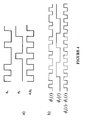
- Exemplary sets of acceptable waveforms are presented in Figures 4(a) and 4(b), plotted in amplitude versus time.
- Mixing signals are typically presented herein in terms of binary 1 s and 0s, however, bipolar waveforms, ⁇ 1, may also be used.
- Bipolar waveforms are typically used in spread spectrum applications because they use commutating mixers which periodically invert their inputs in step with a local control signal (this inverting process is distinct from mixing a signal with a local oscillator directly).
- the two mixing signals ⁇ 1 and ⁇ 2 in Figure 4(a) satisfy the above criteria. Any frequency component one mixing signal might have around DC or around the centre frequency, f RF , of the input signal x(t) , is suppressed by the other. As well, the product of the two mixing signals is that of the desired LO frequency, so the input signal x(t) will be demodulated or modulated as desired.
- Figure 4(b) presents a second exemplary set of acceptable waveforms, plotted in amplitude versus time. In this case, however, the waveforms repeat on a four cycle pattern.
- the states of these ⁇ 1 and ⁇ 2 signals with respect to the hypothetical ⁇ 1 * ⁇ 2 output are as follows: ⁇ 1 * ⁇ 2 ⁇ 1 ⁇ 2 Cycle 1 - LO LO LO Cycle 1 - HI HI LO Cycle 2 - LO LO LO Cycle 2 - HI HI LO Cycle 3 - LO HI HI Cycle 3 - HI LO HI Cycle 4 - LO HI HI Cycle 4 - LO HI HI Cycle 4 - HI LO HI LO HI
- the topology of the invention is similar to that of two stage or multistage modulators and demodulators, but the use of irregular, time-varying mixer signal provides fundamental advantages over known transmitters and receivers. For example:
- a high level of integration results in decreased IC (integrated circuit) pin counts, decreased signal power loss, decreased IC power requirements, imrproved SNR (signal to noise ratio), improved NF (noise factor), and decreased manufacturing costs and complexity.
- the invention provides the basis for fully integrated communications transmitters and receivers. Increasing levels of integration have been the driving impetus towards lower cost, higher volume, higher reliability and lower power consumer electronics since the inception of the integrated circuit. This invention will enable communications devices to follow the same integration route that other consumer electronic products have benefited from.
- advantages from the perspective of the manufacturer when incorporating the invention into a product include:
- mixer M1I 92 receives the input signal x(t) and mixes it with ⁇ 1I ; subsequent to this, mixer M2I 94 mixes signal x(t) ⁇ 1I with ⁇ 2I to yield the in-phase component of the input signal, that is, x(t) ⁇ 1I ⁇ 2I .
- mixer M1Q 96 receives the input signal x(t) and mixes it with ⁇ 1Q ; after which mixer M2Q 98 mixes signal x(t) ⁇ 1Q with ⁇ 2Q to yield the quadrature phase component of the input signal, that is, x(t) ⁇ 1Q ⁇ 2Q .
- ⁇ 1 and ⁇ 2 The general criteria for ⁇ 1 and ⁇ 2 presented above are suitable for most applications. It follows logically, that the further the ⁇ 1 and ⁇ 2 signals are away from the centre frequency, f RF , of the input signal x(t) , and from the output signal y(t) , the less noise will result.
- PN sequences also referred to as spreading codes, pseudo-random or pseudo-noise
- PN codes are called "pseudo" because they are not real Gaussian noise; while they appear to be random sequences of binary 1s and 0s, or ⁇ 1s, but in fact are perfectly deterministic and periodic. While PN codes have properties which can be exploited by embodiment of the invention, they were clearly developed for an entirely different purpose.
- the essence of a spread spectrum communications system is the process of expanding the signal bandwidth in accordance with a spreading code, transmitting that expanded signal, and then recovering the desired signal by reconstructing the received spread-spectrum signal into the original information bandwidth by application of a corresponding de-spreading code.
- the purpose of this bandwidth trade-off is to allow the system to deliver error-free information in a hostile signal environment.
- PN sequences Two of the properties of PN sequences that make them effective in spread spectrum communications are their auto-correlation and cross-correlation properties. These auto-correlation and cross-correlation properties also make PN sequences well suited for use in the mixer of the invention.
- Auto-correlation is the degree of correspondence between a sequence and a phase shifted replica of itself. In a spread-spectrum application, this helps avoid false synchronization. When applied to the invention, this property results in a broad distribution of power across the frequency spectrum.
- Cross-correlation is the measure of similarity between two different PN codes. In a spread-spectrum application, this helps signals from being confused with one another. In the context of the invention, signals with good cross-correlation will have very different power spectra. Thus, they will not emphasize images and intermodulation products generated by one another, and in fact, will suppress them.
- Pseudo-random noise (PN) codes are generally designed to optimise auto-correlation and cross-correlation in view of the number of codes desired in an application.
- rows 5 and 6 of the H 8 matrix are the signals presented in Figure 4(b).
- Other suitable pairings of an H 8 Hadamard matrix are rows 3 and 4, and rows 7 and 8.
- PN sequences can be generated using binary linear feedback shift register (LFSR) and syncopated-register circuits as known in the art.
- LFSR circuits are constructed using a series of shift registers, modulo 2 adders (XOR gates) and feedback loops.
- Syncopated-register circuits are particularly useful because they allow the use of two or more slow generators to produce high rate sequences.
- An initial sequence or seed must be loaded into the LFSR, otherwise the shift register series would simply cycle 0s through itself.
- This seed can be stored in a ROM (read only memory) or processor, or set using DIP (dual in-line package) switches or jumpers.
- the maximum length of a PN sequence is determined by the length of the register chain and the configuration of the feedback network.
- An n-bit register can provide up to 2" different combinations of zeros and ones.
- PN codes may also be generated using field programmable gate arrays (FPGAs), programmable array logic (PALs), read only memories (ROMs), microcontrollers, digital signal processors (DSPs), microprocessors or other devices known in the art.
- FPGAs field programmable gate arrays
- PALs programmable array logic
- ROMs read only memories
- DSPs digital signal processors
- the PN code generating components could be integrated with the rest of the invention into an ASIC (Application Specific Integrated Circuit).
- ASIC Application Specific Integrated Circuit
- PN sequences There are a number of widely used PN sequences known in the art, including Walsh-Hadamard codes, Gold codes and Kasami codes.
- Gold codes for example, are generated by adding together the output of two LFSR sequence generators.
- PN codes are "balanced", that is, they do not have an equal number of 0s and 1s (or +1s and -1s). All PN codes with an odd number of bits, for example, cannot be balanced. Also, Gold codes do not average to zero.
- the mixing signals used in the implementation of the invention be balanced in order to satisfy the conditions outlined hereinabove under the heading "Preferred Criteria for ⁇ 1 and ⁇ 2 ". If unbalanced PN codes are used to implement the invention, it is preferred that such codes be modified by inserting additional 0s and 1s. The locations of these additional 0s and 1s must be carefully determined to maintain the requirement of ⁇ 1 (t) * ⁇ 2 (t) having a frequency component at the RF carrier frequency.
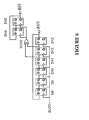
- the synthesizer 100 presented in Figure 6 uses an input square wave (2LO) at twice the frequency of the RF carrier of the signal being modified to produce the signals ⁇ 1 (t) and ⁇ 2 (t).
- the D-latches D8 through D13 form a shift register which is clocked by the signal 2LO. Since this circuit uses an oscillator at twice the carrier frequency of the input signal, there is no LO signal to leak to the output or into other parts of the circuit.
- none of the intermediate signals, nor either of the mixer signals ⁇ 1 (t) and ⁇ 2 (t) has an LO frequency component.
- the shift register can be initially loaded with a predetermined sequence and the output ⁇ 1 will cycle through that sequence producing the desired output.
- the second output ⁇ 2 is then produced by taking the output of consecutive taps from the shift register, and exclusive-ORing them together with gate XOR2 to produce a signal that can be used to clock a second shift register (D14 and D15).
- the output of the second shift register is then ⁇ 2 .
- this circuit will repeatedly output a signal that consists of six-bits at the 2LO frequency.
- Typical LFSR circuits have feedback loops that generate far longer bit strings before they repeat.
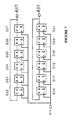
- Figure 7 shows a method similar to that of Figure 6 , except that signal ⁇ 2 is generated by a second shift register (D22 through D27), which is a duplicate of the shift register that produces the signal ⁇ 1 (D16 through D21 ).
- a second shift register (D22 through D27)
- D22 through D27 is a duplicate of the shift register that produces the signal ⁇ 1 (D16 through D21 ).
- the first shift register being loaded with the sequence that will produce ⁇ 1
- the second being loaded with the sequence which will produce ⁇ 2 .
- FIG. 8 An example of a shift register circuit which generates a longer bit string before repeating, is presented in the block diagram of Figure 8 .
- the D-latches D29 through D32 form a shift register which is clocked by the signal at twice the RF carrier frequency.
- MOD1 does a modulo-2 multiplication of the output of D31 with the output of D32, which is then fed into the input of D32 to produce the required feedback.
- the signal ⁇ 2 is then produced at the output of D32.
- a similar shift register with similar feedback can be used to produce the signal ⁇ 1 .
- Unwanted signals may arrive at the receiver or transmitter via many different paths. As these unwanted signals are mixed with the VLO signals, aliasing of out of band power into the signal spectrum may occur. The complementary mixing along the mixing path will remove much of this unwanted signal power from the bandwidth of the desired signal, but a portion of the aliased power may remain within the bandwidth of the output desired signal.
- This aliasing power can be reduced in several manners, including the following:
- DC noise signals will be generated by the direct conversion process, and interfere with low-frequency information contained in the demodulated baseband signal.
- These DC noise signals are particularly difficult to overcome because they are typically unpredictable and time varying.
- Exemplary mechanisms which may generate such DC signals include the following:
- DC offset may or may not be a significant problem.
- the level of these DC signals may be reduced or compensated for in a number of manners:
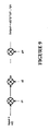
- FIG 3 two mixer signals are used to perform the down-conversion or up-conversion of x(t) . It is also possible to use more than two signals to accomplish the same goal.
- the block diagram of Figure 9 presents such a variation, where several functions ⁇ 1 , ⁇ 2 , ⁇ 3 ... ⁇ n are used to generate the virtual LO.
- ⁇ 1 * ⁇ 2 *... * ⁇ n has a significant power level at the LO frequency being emulated
- the grouping of the functions ⁇ 1 ... ⁇ n are complementary in that they suppress power from one another, within the bandwidth of the input signal x(t) , and within the bandwidth of the output signal.
- the invention consists of m parallel signal paths in which each signal path can be modelled as n mixers operating in series.
- the outputs of the m signal paths are combined into a single output signal y(t) via mixers M w1 through M wm , and the summer.
- Each mixer path is modulated by a weighting factor, ⁇ w1 through ⁇ wm .
- the weighting factors could be binary, in that one or more particular signal paths are chosen at a time, or may modulate the amplitude of the various signal paths before mixing.
- each mixer path could be supplied with a different set of mixer signals ⁇ 1x through ⁇ nx' and mixer paths be chosen which optimise certain desired parameters (for example, maximizing amplitude of the output signal, minimizing interference, etc.).
- these weighing factors may vary with time.
- the invention allows one to fully integrate a RF transmitter on a single chip without using external filters. Furthermore, the RF transmitter can be used as a multi-standard transmitter because new mixing sequences can easily be generated. This is in contrast to existing mixer systems which are typically hard wired.
- the electrical circuits of the invention may be described by computer software code in a simulation language, or hardware development language used to fabricate integrated circuits.
- This computer software code may be stored in a variety of formats on various electronic memory media including computer diskettes, CD-ROM, Random Access Memory (RAM) and Read Only Memory (ROM).
- electronic signals representing such computer software code may also be transmitted via a communication network.
- Such computer software code may also be integrated with the code of other programs, implemented as a core or subroutine by external program calls, or by other techniques known in the art.
- Such signals may be generated using conventional methods and components including basic logic gates, field programmable gate arrays (FPGAs), programmable array logic (PALs) or gate array logic (GALs).
- the signals of the invention may also be stored on memory devices such as read only memories (ROMs), programmable read only memories (PROMs), erasable programmable read only memories (EPROMs), electrically erasable programmable read only memories (EEPROMs) or flash memory, and cycled out as required.
- ROMs read only memories
- PROMs programmable read only memories
- EPROMs erasable programmable read only memories
- EEPROMs electrically erasable programmable read only memories
- flash memory and cycled out as required.
- the embodiments of the invention may also be implemented using processor-type devices such as digital signal processors (DSPs), microcontrollers, microprocessors, or similar devices as known in the art. Such implementations would be clear to one skilled in the art.
- the invention may be applied to various communication protocols and formats including: amplitude modulation (AM), frequency modulation (FM), frequency shift keying (FSK), phase shift keying (PSK), cellular telephone systems including analogue and digital systems such as code division multiple access (CDMA), time division multiple access (TDMA) and frequency division multiple access (FDMA).
- AM amplitude modulation
- FM frequency modulation
- FSK frequency shift keying
- PSK phase shift keying
- CDMA code division multiple access
- TDMA time division multiple access
- FDMA frequency division multiple access
- wired communication systems include computer communication systems such as local area networks (LANs), point to point signalling, and wide area networks (WANs) such as the Internet, using electrical or optical fibre cable systems.
- wireless communication systems may include those for public broadcasting such as AM and FM radio, and UHF and VHF television; or those for private communication such as cellular telephones, personal paging devices, wireless local loops, monitoring of homes by utility companies, cordless telephones including the digital cordless European telecommunication (DECT) standard, mobile radio systems, GSM and AMPS cellular telephones, microwave backbone networks, interconnected appliances under the Bluetooth standard, and satellite communications.
- DECT digital cordless European telecommunication
Landscapes
- Engineering & Computer Science (AREA)
- Computer Networks & Wireless Communication (AREA)
- Signal Processing (AREA)
- Power Engineering (AREA)
- Superheterodyne Receivers (AREA)
- Radar Systems Or Details Thereof (AREA)
- Burglar Alarm Systems (AREA)
Claims (26)
- Ein Synthesizer zur Erzeugung von Signalen, welche sukzessiven Mischern zur Modulation oder Demodulation eines Eingangssignals x(t) in eine Ausgabe y(t) zugeführt werden, wobei der Synthesizer umfasst:einen ersten Signalgenerator zur Erzeugung eines ersten zeitvariierenden Signals ϕ1, wobei das erste zeitvariierende Signal ϕ1 einem ersten der sukzessiven Mischer zugeführt wird, um das Eingangssignal x(t) mit dem ersten zeitvariierenden Signal ϕ1 zu mischen, um ein x(t) * ϕ1 Signal zu erzeugen; undeinem zweiten Signalgenerator zur Erzeugung eines zweiten zeitvariierenden Signals ϕ2, wobei das zweite zeitvariierende Signal ϕ2 einem zweiten der sukzessiven Mischer zugeführt wird, um das x(t) * ϕ1 Signal mit dem zweiten zeitvariierenden Signal ϕ2 zu mischen, um die Ausgabe y(t) zu erzeugen; undwobei ϕ1 * ϕ2 eine signifikante Leistung bei der Frequenz eines emulierten Lokal-Oszillatorsignals aufweist, und wobei einer der ϕ1 und ϕ2 eine minimale Leistung im Bereich der Frequenz der Ausgabe y(t) aufweist, während der andere der ϕ1 und ϕ2 eine minimale Leistung im Bereich der Mittenfrequenz fRF des Eingangssignals x(t) aufweist.
- Der Synthesizer nach Anspruch 1, wobei die Leistung von ϕ1 im Bereich der Frequenz der Ausgabe y(t) auf ein Minimum gebracht ist und wobei die Leistung von ϕ2 im Bereich der Mittenfrequenz fRF des Eingangssignals x(t) auf ein Minimum gebracht ist.
- Der Synthesizer nach Anspruch 1, wobei die Leistung von ϕ2 im Bereich der Frequenz der Ausgabe y(t) auf ein Minimum gebracht ist und wobei die Leistung von ϕ1 im Bereich der Mittenfrequenz fRF des Eingangssignals x(t) auf ein Minimum gebracht ist.
- Der Synthesizer nach Anspruch 1 zur Demodulation des Eingangssignals x(t) in das Basisband, wobei die Leistung von ϕ1 im Bereich von DC auf ein Minimum gebracht ist, und wobei die Leistung von ϕ2 im Bereich der Mittenfrequenz fRF des Eingangssignals x(t) auf ein Minimum gebracht ist.
- Der Synthesizer nach Anspruch 1 zur Demodulation des Eingangssignals x(t) in das Basisband, wobei die Leistung von ϕ2 im Bereich von DC auf ein Minimum gebracht ist und wobei die Leistung von ϕ1 im Bereich der Mittenfrequenz fRF des Eingangssignals x(t) auf ein Minimum gebracht ist.
- Der Synthesizer nach Anspruch 4, wobei die Leistung von ϕ1 im Frequenzbereich von DC bis DC plus der Bandbreite BW des Eingangssignals x(t) geringer ist als die Leistung von ϕ1 bei Frequenzen, die größer sind als DC plus BW, und wobei die Leistung von ϕ2 im Frequenzbereich von fRF - BW/2 und fRF + BW/2 geringer ist als die Leistung von ϕ2 bei Frequenzen, die größer sind als fRF + BW.
- Der Synthesizer nach Anspruch 5, wobei die Leistung von ϕ2 im Frequenzbereich von DC bis DC plus der Bandbreite BW des Eingangssignals x(t) geringer ist als die Leistung von ϕ2 bei Frequenzen, die größer sind als DC plus BW, und wobei die Leistung von ϕ1 im Frequenzbereich von fRF - BW/2 und fRF + BW/2 geringer ist als die Leistung von ϕ1 bei Frequenzen, die größer sind als fRF + BW.
- Der Synthesizer nach Anspruch 4, wobei gilt:

und
wobei Δf geringer ist als BW. - Synthesizer nach Anspruch 5, wobei gilt:

und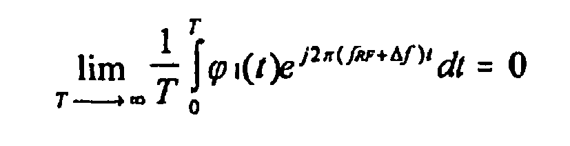
wobei Δf geringer ist als BW. - Der Synthesizer nach Anspruch 4, wobei gilt:
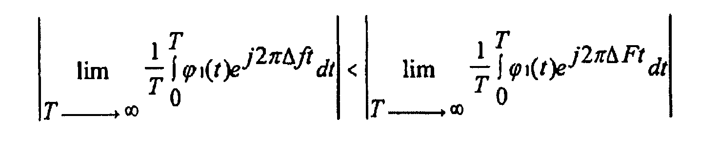
wobei Δf < BW und ΔF > BW ist; und wobei gilt:
wobei Δf < BW und ΔF > BW ist. - Der Synthesizer nach Anspruch 5, wobei gilt:
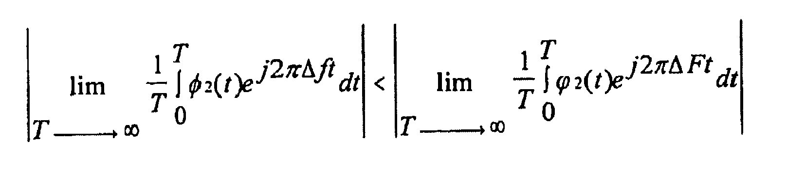
wobei Δf < BW und ΔF > BW ist; und wobei gilt:
wobei Δf < BW und ΔF > BW ist. - Der Synthesizer nach Anspruch 1, wobei das erste und das zweite zeitvariierende Signal mittels linear rückgekoppelte Schieberegister-Schaltungen (LFSR- Schaltungen) erzeugt werden.
- Der Synthesizer nach Anspruch 1, wobei der erste und der zweite Signalgenerator umfassen:Schieberegistermittel zur Erzeugung des ersten und des zweiten zeitvariierenden Signals ϕ1 und ϕ2, indem korrespondierende, vorher festgelegte Sequenzen umgeschaltet werden.
- Der Synthesizer nach Anspruch 13, wobei die Schieberegistermittel umfassen:ein Schieberegister, um ein Oszillatorsignal bei einer Frequenz zu empfangen, die zweimal so hoch ist wie die Frequenz des emulierten Lokal-Oszillatorsignals, um das erste zeitvariierende Signal ϕ1 zu erzeugen, indem korrespondierende, vorher festgelegte Sequenzen umgeschaltet werden.
- Der Synthesizer nach Anspruch 13, wobei der erste Signalgenerator ein Schieberegister mit einer Rückkopplungsschleife umfasst.
- Der Synthesizer nach Anspruch 1, wobei
ein zusätzlicher oder mehrere zusätzliche Signalgeneratoren zum Erzeugen von einem oder mehreren zusätzlichen zeitvariierenden Signalen vorgesehen sind;
wobei das Produkt aller zeitvariierenden Signale eine signifikante Leistung bei der Frequenz des emulierten Lokal-Oszillatorsignals aufweist; und wobei keines der zeitvariierenden Signale eine signifikante Leistung bei der Frequenz des emulierten Lokal-Oszillatorsignals aufweist. - Der Synthesizer nach Anspruch 1, wobei Mittel zur Vorfilterung vorgesehen sind, um die Aliasingleistung zu reduzieren.
- Der Synthesizer nach Anspruch 17, wobei τ/T der Mittel zur Vorfilterung auf ein Minimum gebracht wird, um die Aliasingleistung zu reduzieren.
- Der Synthesizer nach Anspruch 1, wobei Mittel zur Flankenplatzierung vorgesehen sind, um die Aliasingleistung zu reduzieren.
- Der Synthesizer nach Anspruch 1, wobei Mittel zur Gleichstrom-Offset (DC-Offset) Korrektur vorgesehen sind.
- Der Synthesizer nach Anspruch 20, wobei das Mittel zur Gleichstrom-Offset Korrektur Kopplungskondensatoren umfasst.
- Der Synthesizer nach Anspruch 20, wobei das Mittel zur Gleichstrom - Offset Korrektur Mittel zur anpassungsfähigen Rückkopplung umfasst.
- Der Synthesizer nach Anspruch 1, weiter mit einem einzelnen Oszillator zur Erzeugung des ersten zeitvariierenden Signals ϕ1 und des zweiten zeitvariierenden Signals ϕ2.
- Ein Modulator oder Demodulator, umfassend:mehrere Mischkanäle, wobei jeder Mischkanalzwei Mischer,einen ersten Signalgenerator zum Erzeugen eines ersten zeitvariierenden Signals ϕ1 und einen zweiten Signalgenerator zum Erzeugen eines zweiten zeitvariierenden Signals ϕ2 aufweist,wobei ϕ1 * ϕ2 eine signifikante Leistung bei der Frequenz eines emulierten Lokal-Oszillatorsignals aufweist, und wobei einer der ϕ1 und ϕ2 eine minimale Leistung im Bereich der Frequenz der Ausgabe y(t) aufweist, während der andere der ϕ1 und ϕ2 eine minimale Leistung im Bereich der Mittenfrequenz fRF des Eingangssignals x(t) aufweist; und einen gewichteten Addierer zum Empfangen der Ausgabe der einzelnen Mischkanäle und zum Kombinieren eines gewichteten Faktors der jeweiligen Ausgabe.
- Der Modulator oder Demodulator nach Anspruch 24, wobei die Gewichtungsfaktoren über die Zeit variieren.
- Ein Verfahren zur Modulation oder Demodulation eines Eingangssignals x(t) in eine Ausgabe y(t), wobei das Verfahren die folgenden Schritte aufweist:Erzeugung eines ersten zeitvariierenden Signals ϕ1;Erzeugung eines zweiten zeitvariierenden Signals ϕ2, wobei ϕ1 * ϕ2 eine signifikante Leistung bei der Frequenz eines emulierten Lokal-Oszillatorsignals aufweist, und wobei einer der ϕ1 und ϕ2 eine minimale Leistung im Bereich der Frequenz der Ausgabe y(t) aufweist, während der andere der ϕ1 und ϕ2 eine minimale Leistung im Bereich der Mittenfrequenz fRF des Eingangssignals x(t) aufweist;Mischen des ersten Eingangssignals x(t) mit dem ersten zeitvariierenden Signal ϕ1, um ein x(t) * ϕ1 Signal zu erzeugen; undMischen des x(t) * ϕ1 Signals mit dem zweiten zeitvariierenden Signal ϕ2, um die Ausgabe y(t) zu erzeugen.
Applications Claiming Priority (7)
| Application Number | Priority Date | Filing Date | Title |
|---|---|---|---|
| WOPCT/CA00/00996 | 2000-09-01 | ||
| PCT/CA2000/000996 WO2001017122A1 (en) | 1999-09-01 | 2000-09-01 | Improved method and apparatus for up- and down-conversion of radio frequency (rf) signals |
| PCT/CA2000/000994 WO2001017120A2 (en) | 1999-09-01 | 2000-09-01 | Freqency translator using a non-periodic local oscillator signal |
| WOPCT/CA00/00995 | 2000-09-01 | ||
| PCT/CA2000/000995 WO2001017121A1 (en) | 1999-09-01 | 2000-09-01 | Improved method and apparatus for up-conversion of radio frequency (rf) signals |
| WOPCT/CA00/00994 | 2000-09-01 | ||
| PCT/CA2001/000876 WO2002019548A2 (en) | 2000-09-01 | 2001-06-19 | Improved method and apparatus for up- and down- conversion of radio frequency (rf) signals |
Publications (2)
| Publication Number | Publication Date |
|---|---|
| EP1314255A2 EP1314255A2 (de) | 2003-05-28 |
| EP1314255B1 true EP1314255B1 (de) | 2009-10-21 |
Family
ID=27168651
Family Applications (1)
| Application Number | Title | Priority Date | Filing Date |
|---|---|---|---|
| EP01944827A Expired - Lifetime EP1314255B1 (de) | 2000-09-01 | 2001-06-19 | Verbesserte verfahren und vorrichtung zur auf- und abwärtsumsetzung von hochfrequenzsignalen (rf) |
Country Status (6)
| Country | Link |
|---|---|
| EP (1) | EP1314255B1 (de) |
| AT (1) | ATE446613T1 (de) |
| AU (1) | AU2001267222A1 (de) |
| CA (1) | CA2421173A1 (de) |
| DE (1) | DE60140261D1 (de) |
| WO (1) | WO2002019548A2 (de) |
Families Citing this family (1)
| Publication number | Priority date | Publication date | Assignee | Title |
|---|---|---|---|---|
| CA2375291C (en) * | 2002-03-08 | 2005-05-17 | Sirific Wireless Corporation | Generation of virtual local oscillator inputs for use in direct conversion radio systems |
Family Cites Families (9)
| Publication number | Priority date | Publication date | Assignee | Title |
|---|---|---|---|---|
| DE2627586C3 (de) * | 1976-06-19 | 1980-03-13 | Carl Schenck Ag, 6100 Darmstadt | Verfahren und Schaltungsanordnung zur Multiplikation von elektrischen Wechselspannungssignalen |
| US5390346A (en) * | 1994-01-21 | 1995-02-14 | General Instrument Corporation Of Delaware | Small frequency step up or down converters using large frequency step synthesizers |
| AU2909795A (en) * | 1994-06-29 | 1996-01-25 | Honeywell Inc. | Spurious response rejecting mixer using spread spectrum techniques |
| JP2737655B2 (ja) * | 1994-07-12 | 1998-04-08 | 双葉電子工業株式会社 | スペクトル拡散通信方式 |
| US5956345A (en) * | 1996-09-13 | 1999-09-21 | Lucent Technologies Inc. | IS-95 compatible wideband communication scheme |
| JP3651154B2 (ja) * | 1996-12-27 | 2005-05-25 | ソニー株式会社 | Pn符号発生回路及び無線システムの端末装置 |
| KR100264862B1 (ko) * | 1997-07-31 | 2000-09-01 | 윤종용 | 대역확산에따른직교부호도약다중접속방식통신시스템의송수신장치및그방법 |
| CN1211969C (zh) * | 1997-09-13 | 2005-07-20 | 三星电子株式会社 | 用于双正交码跳变多址通信系统的设备和方法 |
| EP0977351B1 (de) * | 1998-07-30 | 2004-02-18 | Motorola Semiconducteurs S.A. | Verfahren und Gerät zur Funkübertragung |
-
2001
- 2001-06-19 EP EP01944827A patent/EP1314255B1/de not_active Expired - Lifetime
- 2001-06-19 CA CA002421173A patent/CA2421173A1/en not_active Abandoned
- 2001-06-19 WO PCT/CA2001/000876 patent/WO2002019548A2/en not_active Ceased
- 2001-06-19 AU AU2001267222A patent/AU2001267222A1/en not_active Abandoned
- 2001-06-19 AT AT01944827T patent/ATE446613T1/de not_active IP Right Cessation
- 2001-06-19 DE DE60140261T patent/DE60140261D1/de not_active Expired - Lifetime
Also Published As
| Publication number | Publication date |
|---|---|
| AU2001267222A1 (en) | 2002-03-13 |
| ATE446613T1 (de) | 2009-11-15 |
| EP1314255A2 (de) | 2003-05-28 |
| WO2002019548A3 (en) | 2002-12-27 |
| WO2002019548A2 (en) | 2002-03-07 |
| DE60140261D1 (de) | 2009-12-03 |
| CA2421173A1 (en) | 2002-03-07 |
Similar Documents
| Publication | Publication Date | Title |
|---|---|---|
| US7046980B1 (en) | Method and apparatus for up-and down-conversion of radio frequency (RF) signals | |
| US7277683B2 (en) | Regenerative divider for up and down conversion of radio frequency (RF) signals | |
| JP4335135B2 (ja) | 複数の局部発振器を有する改善されたミキサおよびこれに基づくシステム | |
| JP2008178135A (ja) | 無線受信回路、無線送信回路および無線受信回路を動作させる方法 | |
| US6449471B1 (en) | Wireless terminal device | |
| US7215931B2 (en) | Method and apparatus for up-and-down-conversion of radio frequency (RF) signals | |
| US20050226349A1 (en) | Down conversion methodology and topology which compensates for spurious response | |
| US10804974B2 (en) | N-path mixer-based receiver apparatus and method with transmitter self-interference rejection | |
| EP1479171A1 (de) | Verfahren und vorrichtung zur abwärtsumsetzung von radiofrequenzsignalen | |
| US6727764B2 (en) | Generation of virtual local oscillator inputs for use in direct conversion radio systems | |
| CA2375291C (en) | Generation of virtual local oscillator inputs for use in direct conversion radio systems | |
| EP1590886B1 (de) | Abwärtsumsetzung von Radiofrequenzen (RF)-Signalen | |
| KR20010111051A (ko) | 직접 변환 수신기 및 송수신기 | |
| EP1314255B1 (de) | Verbesserte verfahren und vorrichtung zur auf- und abwärtsumsetzung von hochfrequenzsignalen (rf) | |
| CA2381999C (en) | Improved method and apparatus for up- and down- conversion of radio frequency (rf) signals | |
| US20020094794A1 (en) | Method and apparatus for conversion of radio frequency (RF) and baseband signals | |
| US6980785B1 (en) | Direct conversion wireless receiver with digital phase equalization | |
| EP1089446A1 (de) | Funkendgerät | |
| EP1111772B1 (de) | Verfahren und Vorrichtung zum verbesserten Schutz gegen der Intermodulationsverzerrung | |
| EP1170875B1 (de) | Radio Architektur zur Verringerung der Senderinterferenz | |
| CA2511819A1 (en) | Regenerative divider for up and down conversion of radio frequency (rf) signals | |
| Zolfaghari | Transceiver Architecture |
Legal Events
| Date | Code | Title | Description |
|---|---|---|---|
| PUAI | Public reference made under article 153(3) epc to a published international application that has entered the european phase |
Free format text: ORIGINAL CODE: 0009012 |
|
| 17P | Request for examination filed |
Effective date: 20030319 |
|
| AK | Designated contracting states |
Designated state(s): AT BE CH CY DE DK ES FI FR GB GR IE IT LI LU MC NL PT SE TR |
|
| AX | Request for extension of the european patent |
Extension state: AL LT LV MK RO SI |
|
| RIN1 | Information on inventor provided before grant (corrected) |
Inventor name: WONG, LAWRENCE Inventor name: MANKU, TAJINDER Inventor name: WEALE, GARETH Inventor name: SNYDER, CHRIS |
|
| RIN1 | Information on inventor provided before grant (corrected) |
Inventor name: SNYDER, CHRIS Inventor name: WEALE, GARETH Inventor name: MANKU, TAJINDER Inventor name: WONG, LAWRENCE |
|
| GRAP | Despatch of communication of intention to grant a patent |
Free format text: ORIGINAL CODE: EPIDOSNIGR1 |
|
| RAP1 | Party data changed (applicant data changed or rights of an application transferred) |
Owner name: ICERA CANADA ULC |
|
| GRAS | Grant fee paid |
Free format text: ORIGINAL CODE: EPIDOSNIGR3 |
|
| GRAA | (expected) grant |
Free format text: ORIGINAL CODE: 0009210 |
|
| AK | Designated contracting states |
Kind code of ref document: B1 Designated state(s): AT BE CH CY DE DK ES FI FR GB GR IE IT LI LU MC NL PT SE TR |
|
| AX | Request for extension of the european patent |
Extension state: AL LT LV MK RO SI |
|
| REG | Reference to a national code |
Ref country code: GB Ref legal event code: FG4D |
|
| REG | Reference to a national code |
Ref country code: CH Ref legal event code: EP |
|
| REG | Reference to a national code |
Ref country code: IE Ref legal event code: FG4D |
|
| REF | Corresponds to: |
Ref document number: 60140261 Country of ref document: DE Date of ref document: 20091203 Kind code of ref document: P |
|
| LTIE | Lt: invalidation of european patent or patent extension |
Effective date: 20091021 |
|
| PG25 | Lapsed in a contracting state [announced via postgrant information from national office to epo] |
Ref country code: SE Free format text: LAPSE BECAUSE OF FAILURE TO SUBMIT A TRANSLATION OF THE DESCRIPTION OR TO PAY THE FEE WITHIN THE PRESCRIBED TIME-LIMIT Effective date: 20091021 Ref country code: PT Free format text: LAPSE BECAUSE OF FAILURE TO SUBMIT A TRANSLATION OF THE DESCRIPTION OR TO PAY THE FEE WITHIN THE PRESCRIBED TIME-LIMIT Effective date: 20100222 Ref country code: FI Free format text: LAPSE BECAUSE OF FAILURE TO SUBMIT A TRANSLATION OF THE DESCRIPTION OR TO PAY THE FEE WITHIN THE PRESCRIBED TIME-LIMIT Effective date: 20091021 Ref country code: ES Free format text: LAPSE BECAUSE OF FAILURE TO SUBMIT A TRANSLATION OF THE DESCRIPTION OR TO PAY THE FEE WITHIN THE PRESCRIBED TIME-LIMIT Effective date: 20100201 |
|
| PG25 | Lapsed in a contracting state [announced via postgrant information from national office to epo] |
Ref country code: AT Free format text: LAPSE BECAUSE OF FAILURE TO SUBMIT A TRANSLATION OF THE DESCRIPTION OR TO PAY THE FEE WITHIN THE PRESCRIBED TIME-LIMIT Effective date: 20091021 Ref country code: BE Free format text: LAPSE BECAUSE OF FAILURE TO SUBMIT A TRANSLATION OF THE DESCRIPTION OR TO PAY THE FEE WITHIN THE PRESCRIBED TIME-LIMIT Effective date: 20091021 |
|
| PG25 | Lapsed in a contracting state [announced via postgrant information from national office to epo] |
Ref country code: DK Free format text: LAPSE BECAUSE OF FAILURE TO SUBMIT A TRANSLATION OF THE DESCRIPTION OR TO PAY THE FEE WITHIN THE PRESCRIBED TIME-LIMIT Effective date: 20091021 |
|
| PLBE | No opposition filed within time limit |
Free format text: ORIGINAL CODE: 0009261 |
|
| STAA | Information on the status of an ep patent application or granted ep patent |
Free format text: STATUS: NO OPPOSITION FILED WITHIN TIME LIMIT |
|
| 26N | No opposition filed |
Effective date: 20100722 |
|
| PG25 | Lapsed in a contracting state [announced via postgrant information from national office to epo] |
Ref country code: GR Free format text: LAPSE BECAUSE OF FAILURE TO SUBMIT A TRANSLATION OF THE DESCRIPTION OR TO PAY THE FEE WITHIN THE PRESCRIBED TIME-LIMIT Effective date: 20100122 |
|
| PG25 | Lapsed in a contracting state [announced via postgrant information from national office to epo] |
Ref country code: MC Free format text: LAPSE BECAUSE OF NON-PAYMENT OF DUE FEES Effective date: 20100630 |
|
| REG | Reference to a national code |
Ref country code: CH Ref legal event code: PL |
|
| PG25 | Lapsed in a contracting state [announced via postgrant information from national office to epo] |
Ref country code: IT Free format text: LAPSE BECAUSE OF FAILURE TO SUBMIT A TRANSLATION OF THE DESCRIPTION OR TO PAY THE FEE WITHIN THE PRESCRIBED TIME-LIMIT Effective date: 20091021 |
|
| PG25 | Lapsed in a contracting state [announced via postgrant information from national office to epo] |
Ref country code: CH Free format text: LAPSE BECAUSE OF NON-PAYMENT OF DUE FEES Effective date: 20100630 Ref country code: IE Free format text: LAPSE BECAUSE OF NON-PAYMENT OF DUE FEES Effective date: 20100619 Ref country code: LI Free format text: LAPSE BECAUSE OF NON-PAYMENT OF DUE FEES Effective date: 20100630 |
|
| PGFP | Annual fee paid to national office [announced via postgrant information from national office to epo] |
Ref country code: FR Payment date: 20110617 Year of fee payment: 11 |
|
| PG25 | Lapsed in a contracting state [announced via postgrant information from national office to epo] |
Ref country code: CY Free format text: LAPSE BECAUSE OF FAILURE TO SUBMIT A TRANSLATION OF THE DESCRIPTION OR TO PAY THE FEE WITHIN THE PRESCRIBED TIME-LIMIT Effective date: 20091021 |
|
| PG25 | Lapsed in a contracting state [announced via postgrant information from national office to epo] |
Ref country code: LU Free format text: LAPSE BECAUSE OF NON-PAYMENT OF DUE FEES Effective date: 20100619 |
|
| PG25 | Lapsed in a contracting state [announced via postgrant information from national office to epo] |
Ref country code: TR Free format text: LAPSE BECAUSE OF FAILURE TO SUBMIT A TRANSLATION OF THE DESCRIPTION OR TO PAY THE FEE WITHIN THE PRESCRIBED TIME-LIMIT Effective date: 20091021 |
|
| REG | Reference to a national code |
Ref country code: FR Ref legal event code: ST Effective date: 20130228 |
|
| REG | Reference to a national code |
Ref country code: DE Ref legal event code: R082 Ref document number: 60140261 Country of ref document: DE Representative=s name: KEIL & SCHAAFHAUSEN PATENT- UND RECHTSANWAELTE, DE |
|
| PG25 | Lapsed in a contracting state [announced via postgrant information from national office to epo] |
Ref country code: FR Free format text: LAPSE BECAUSE OF NON-PAYMENT OF DUE FEES Effective date: 20120702 |
|
| REG | Reference to a national code |
Ref country code: GB Ref legal event code: 732E Free format text: REGISTERED BETWEEN 20130502 AND 20130508 |
|
| REG | Reference to a national code |
Ref country code: DE Ref legal event code: R082 Ref document number: 60140261 Country of ref document: DE Representative=s name: KEIL & SCHAAFHAUSEN PATENT- UND RECHTSANWAELTE, DE Effective date: 20130415 Ref country code: DE Ref legal event code: R081 Ref document number: 60140261 Country of ref document: DE Owner name: NVIDIA TECHNOLOGY UK LIMITED, GB Free format text: FORMER OWNER: ICERA CANADA ULC, CALGARY, CA Effective date: 20130415 Ref country code: DE Ref legal event code: R081 Ref document number: 60140261 Country of ref document: DE Owner name: NVIDIA TECHNOLOGY UK LIMITED, GB Free format text: FORMER OWNER: ICERA CANADA ULC, CALGARY, ALBERTA, CA Effective date: 20130415 |
|
| REG | Reference to a national code |
Ref country code: NL Ref legal event code: SD Effective date: 20130806 |
|
| PGFP | Annual fee paid to national office [announced via postgrant information from national office to epo] |
Ref country code: NL Payment date: 20200525 Year of fee payment: 20 Ref country code: DE Payment date: 20200519 Year of fee payment: 20 |
|
| PGFP | Annual fee paid to national office [announced via postgrant information from national office to epo] |
Ref country code: GB Payment date: 20200525 Year of fee payment: 20 |
|
| REG | Reference to a national code |
Ref country code: DE Ref legal event code: R071 Ref document number: 60140261 Country of ref document: DE |
|
| REG | Reference to a national code |
Ref country code: NL Ref legal event code: MK Effective date: 20210618 |
|
| REG | Reference to a national code |
Ref country code: GB Ref legal event code: PE20 Expiry date: 20210618 |
|
| PG25 | Lapsed in a contracting state [announced via postgrant information from national office to epo] |
Ref country code: GB Free format text: LAPSE BECAUSE OF EXPIRATION OF PROTECTION Effective date: 20210618 |