EP1316115B1 - Technique de catalyseur metallique pour texturer des piles solaires au silicium - Google Patents
Technique de catalyseur metallique pour texturer des piles solaires au silicium Download PDFInfo
- Publication number
- EP1316115B1 EP1316115B1 EP01955043A EP01955043A EP1316115B1 EP 1316115 B1 EP1316115 B1 EP 1316115B1 EP 01955043 A EP01955043 A EP 01955043A EP 01955043 A EP01955043 A EP 01955043A EP 1316115 B1 EP1316115 B1 EP 1316115B1
- Authority
- EP
- European Patent Office
- Prior art keywords
- metal
- reactive ion
- chamber
- textured
- silicon
- Prior art date
- Legal status (The legal status is an assumption and is not a legal conclusion. Google has not performed a legal analysis and makes no representation as to the accuracy of the status listed.)
- Expired - Lifetime
Links
Images






Classifications
-
- H—ELECTRICITY
- H10—SEMICONDUCTOR DEVICES; ELECTRIC SOLID-STATE DEVICES NOT OTHERWISE PROVIDED FOR
- H10F—INORGANIC SEMICONDUCTOR DEVICES SENSITIVE TO INFRARED RADIATION, LIGHT, ELECTROMAGNETIC RADIATION OF SHORTER WAVELENGTH OR CORPUSCULAR RADIATION
- H10F77/00—Constructional details of devices covered by this subclass
- H10F77/70—Surface textures, e.g. pyramid structures
-
- H—ELECTRICITY
- H10—SEMICONDUCTOR DEVICES; ELECTRIC SOLID-STATE DEVICES NOT OTHERWISE PROVIDED FOR
- H10F—INORGANIC SEMICONDUCTOR DEVICES SENSITIVE TO INFRARED RADIATION, LIGHT, ELECTROMAGNETIC RADIATION OF SHORTER WAVELENGTH OR CORPUSCULAR RADIATION
- H10F77/00—Constructional details of devices covered by this subclass
- H10F77/70—Surface textures, e.g. pyramid structures
- H10F77/703—Surface textures, e.g. pyramid structures of the semiconductor bodies, e.g. textured active layers
-
- H—ELECTRICITY
- H10—SEMICONDUCTOR DEVICES; ELECTRIC SOLID-STATE DEVICES NOT OTHERWISE PROVIDED FOR
- H10P—GENERIC PROCESSES OR APPARATUS FOR THE MANUFACTURE OR TREATMENT OF DEVICES COVERED BY CLASS H10
- H10P50/00—Etching of wafers, substrates or parts of devices
- H10P50/20—Dry etching; Plasma etching; Reactive-ion etching
- H10P50/28—Dry etching; Plasma etching; Reactive-ion etching of insulating materials
- H10P50/282—Dry etching; Plasma etching; Reactive-ion etching of insulating materials of inorganic materials
- H10P50/283—Dry etching; Plasma etching; Reactive-ion etching of insulating materials of inorganic materials by chemical means
-
- Y—GENERAL TAGGING OF NEW TECHNOLOGICAL DEVELOPMENTS; GENERAL TAGGING OF CROSS-SECTIONAL TECHNOLOGIES SPANNING OVER SEVERAL SECTIONS OF THE IPC; TECHNICAL SUBJECTS COVERED BY FORMER USPC CROSS-REFERENCE ART COLLECTIONS [XRACs] AND DIGESTS
- Y02—TECHNOLOGIES OR APPLICATIONS FOR MITIGATION OR ADAPTATION AGAINST CLIMATE CHANGE
- Y02E—REDUCTION OF GREENHOUSE GAS [GHG] EMISSIONS, RELATED TO ENERGY GENERATION, TRANSMISSION OR DISTRIBUTION
- Y02E10/00—Energy generation through renewable energy sources
- Y02E10/50—Photovoltaic [PV] energy
Definitions
- This invention pertains generally to the field of multicrystalline silicon solar cells and manufacturing techniques directed to yield improvements in optical performance of silicon solar cells. More specifically, the invention pertains to use of reactive ion etching (RIE) in the presence of metal catalysts to texture the surface of silicon solar cell material.
- RIE reactive ion etching
- the techniques described can controllably generate randomly distributed surface features optimally having dimensions comparable, or smaller than solar spectrum wavelengths.
- Multicrystalline silicon is a frequently-used semiconductor substrate in the manufacture of silicon solar cells.
- Single crystal silicon c-Si is also used in manufacture of silicon solar cells, but it has certain disadvantages including the fact that it is more expensive than mc-Si.
- U.S. Patent 6,091,021 describes some aspects of mc-Si solar cell fabrication developed by the present inventors, including use of micromasks (for example, a thin polycrystalline coating such as SiO 2 ) to aid in etched texturing of mc-Si surfaces.
- micromasks for example, a thin polycrystalline coating such as SiO 2
- CRAIGHEAD H.G. et al: "Textured thin-film Si solar selective absorbers using reactive ion etching" Applied Physics Letters, American Institute of Physics, New York, US, vol. 37, no. 7, October 1980 (1980-10), pages 653-655, XP000816486 ISSN: 0003-6951 discloses a method of forming a textured surface on a substrate by generating randomly distributed surface features thereon comprising the step of exposing a surface of said substrate to a reactive ion plasma comprising at least one etchant and particles of metal introduced into the plasma.
- metal "impurities" particles
- RIE reactive ion etching
- tailored texturization can be engineered according to one embodiment by a strategic placement of metal-coated silicon samples at various locations relative to the surface of the silicon wafer inside the RIE chamber.
- suitable metal species include, for example, Cr, Au, Cu, Al, Pd, and Ti.
- desired texturing results and high throughput can be achieved by conditioning the RIE chamber with a suitable choice of metal catalysts.
- This can include, for example, forming a thin layer of metal, or metals on the inner surfaces of the chamber prior to RIE texturing of silicon in the chamber.
- Suitable metal species include those just mentioned in conjunction with the embodiment utilizing metal-coated Si samples.
- Metal thus introduced into the RIE chamber has the effect of introducing "micro-masks” (or microscopic particles of metal) into the RIE environment.
- Metal present in the reaction chamber “catalyzes” the formation of random nanoscale features on the surface of silicon etched in the chamber, thus resulting in an optically-favorable texturing beneficial for solar cell applications.
- Silicon surfaces textured in this fashion include, for example, columnar and pyramidal features with dimensions that can be much smaller than the wavelength of incident light. This sub-wavelength fabrication technology enables creation of a layer of a tailored index of refraction, spanning the range defined by the refractive indices of air and silicon.
- the invention enables fabrication of an optimum anti-reflective layer on, for example, a mc-Si solar cell, to optimize photon absorption over a broad spectral range and enhance solar cell efficiency.
- the processes of the invention induce only slight surface damage to the Si, if any, which does not significantly diminish current extraction from the solar cell. Such damage, if it occurs, can be easily removed without compromising the optically favorable texture features.
- catalyze refers and relate to the enabling or facilitating effect that certain metals have on random texturing of Si, when they are added to the RIE environment. It is not certain, at this time, whether a classic chemical catalysis is involved, wherein the plasma process is changed due to alteration of reaction pathways. Indeed, the precise chemical and/or physical mechanism(s) responsible for the formation of desirable surface texture features evidently mediated by the presence of metal in the chamber are not presently known, although studies aimed at a complete understanding of underlying physical mechanisms are underway.
- an advantage of the invention is that it provides a method forming a textured surface on a substrate by generating randomly distributed surface features thereon, as recited in claim 1 and a method of forming a silicon solar cell as recited in claim 4.
- Another advantage of the invention is that it includes exposing a surface of such substrate to a reactive ion etching plasma comprising at least one etchant and particles of metal introduced into the plasma.
- Another advantage of the invention is that the techniques of the invention result in nanoscale surface texture features having dimensions smaller than the wavelength of light in the solar spectrum (meaning, specifically, light that is capable of causing the photovoltaic effect in silicon solar cells).
- metal catalysts can be introduced in to a reactive ion etching chamber in various ways including by placing discrete metal sources in the chamber in the presence of a substrate to be textured, and pre-conditioning the interior surfaces of a reactive ion etching chamber using, for example, a thin coating of metal.
- the nano-texturing process of the present invention is based on the critical influence of the metal catalysts on the fundamental nature of the random RIE texturing in Si. This metal-assisted process helps achieve highly uniform textures over a wide process range.
- the present process in one embodiment, utilizes nontoxic and inert etchants such as SF 6 and O 2 gases. This allows for safer and lower cost processing in comparison with hazardous etchants, such as Cl 2 gas employed by some researchers, for example, in Japan. Cost savings are associated with using less hazardous etchants. It is noted, however, texturing can be optimized using the metal catalyst process disclosed here when etchants other than SF 6 and O 2 , including those based on chlorine, bromine and fluorine plasma chemistries, are used.
- the invention process produces silicon (e.g., an mc-Si solar cell) with controllable randomly textured feature dimensions either smaller, or comparable to the solar spectrum wavelengths inside the semiconductor surface.
- Silicon textured according to the invention appear black, or grey to the human eye, and scanning electron micrographs (SEMs) show that the textured profiles achieved are a critical function of the metal catalyst used.
- surface texturing is achieved by placing metal-coated small pieces of silicon in the RIE chamber in proximity to a silicon wafer or other silicon substrate.
- silicon wafer is made here to illustrate one type of silicon substrate suited to texturing according to the principles of the invention.
- Other silicon surfaces such as those of actual silicon solar cells or other bulk silicon material, can be textured, as well, according the processes described herein.
- other semiconductor and dielectric materials, including glass can be textured according to the principles described herein.
- Figures 1 (a) - (d) are schematic illustrations showing the influence of Cr in the chamber during RIE-texture processes on round, 4-inch Si wafers.
- the chamber used in generating these results was Plasma-ThermTM 790 reactor.
- a large parameter space matrix consisting of power, pressure, gas ratios, and etch times was investigated. Desirable texturing results were achieved for RF power of - 300 W, SF 6 flow rate - 14 sccm, O 2 flow rate - 16 sccm, chamber pressure - 170 mTorr, and etch time - 15 minutes.
- Figure 1(a) shows the influence on RIE using SF 6 /O 2 single source of Cr 10 (film thickness - 50 nm, on a piece of silicon having dimensions of - 2 cm x 1.5 cm) positioned nearly adjacent to ( ⁇ 1 inch from) the boundary of a 4-inch diameter Si wafer 4.
- Figure 1(a) shows that the Cr-assisted RIE process described above results in an approximately oval textured region 6 .
- the textured surface generally extended over a large proportion of the wafer and was particularly apparent in the region of the wafer closest to the Cr sample. In those regions of the wafer most distant from the metal sample, no significant amount of texturing occurred.
- Figure 1(a) includes width desigations W 1 , W 2 , W 3 , and W 4 to show representative widths (ranging from about 1 mm closest to the Cr source 10 to about 1.5 cm furthest from the Cr source 10) of portions of the non-textured region 8 .
- Figure 1 (b) shows results from a similar test in which three separate Cr sources 12a, 12b, 12c (film thickness - 50 nm, Si dimensions - 5 mm x 5 mm) are approximately evenly spaced around the perimeter of a 4-inch diameter Si wafer 4.
- Figure 1 (b) shows an approximately triangular textured region 6 using Cr-assisted RIE with three samples.
- Figure 1(c) shows a generally rectangular textured area 6 that resulted from using four Cr sources 12 a - d (film thickness - 50 nm, Si dimensions - 5 mm x 5 mm) approximately evenly spaced around the perimeter of a 4-inch diameter Si wafer.
- Widths W 5 - W 8 (ranging between -1.0 and -1.5 cm) are given in the figure to show approximate size of the non-textured region 8 relative to the textured region 6.
- Figure 1(d) shows a generally circularly symmetric pattern achieved by a symmetric placement of 4 Cr sources 16a -16d (film thickness - 50 nm, Si dimensions - 5 mm x 5 mm) on the wafer itself.
- the non-textured region 8 is also shown in each of the Figures 1(b) - 1(d) , just described.
- Figure 1(d) also shows better uniformity of texturing across the wafer by placing sources on the water edge.
- Figures 2(a) and 2(b) show SEM pictures of a textured region created using Cr as the metallic catalyst.
- Figure 2(a) shows a magnification of x100000, the horizontal bar represents a length of 100 nm
- Figure 2(b) shows a magnification of x70000, the horizontal bar represents a length of 200 nm.
- the columnar features shown in the figures, created using Cr-assisted RIE texturing process have diameters of - 20 - 50 nm, separation of - 50 nm, and depths of - 500 nm.
- Figures 3 (a) - (c) show some examples of RIE textures achieved using Al, Ti, and Pd, respectively, as catalysts.
- Al-assisted texturing illustrated in Figure 3(a) , gives rise to columnar profiles
- Ti-assisted RIE illustrated in Figure 3(b)
- Pd-assisted RIE illustrated in Figure 3(c) results in much larger dimensions.
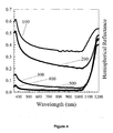
- Figure 4 shows spectral hemispherical reflectance measurements from metal-assisted textured surfaces. Plots are shown for Pd texturing (200), Al texturing (300), Ti texturing (400), and Cr texturing (500). For comparison, reflection from planar Si surface is also plotted (100). It is seen that both Cr and Ti assisted textures have similar reflectance response despite significant variation in their textured profiles. The larger Pd-assisted textures exhibit much higher reflection even though it is still less than that of a planar surface. The Al-assisted texture reflection lies in between Pd and Cr-assisted textures.
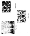
- Figure 5 shows an example of texture obtained for Al samples placed - 3 - 4 inches away from the wafer. Notice that in comparison with the columnar profile shown in Fig. 3(a) , relatively larger features are obtained (on the order of 200 - 500 nm in width, with a separation distance of about 500 nm. These features exhibit longitudinal dimensions of about 500-1000 nm, and larger.
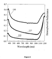
- Figure 6 shows reflectance measurements from two Al-assisted RIE processes. Also in this Figure, for comparison, reflection from planar Si surface is also plotted (100). The plot designated 111 shows hemispherical reflection measurements for Al-assisted random RIE-texured surfaces with the Al source near the wafer. The plot designated 222 shows data for the circumstance in which the Al source is further away from the wafer. It is seen that for Al samples further away from the wafer, significantly lower reflection is achieved. This process also improves texture uniformity and extension over larger wafer regions.
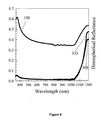
- Figure 8 shows reflectance measurements from these surfaces.
- the plot designated 333 shows results obtained from texturing using the chamber conditioning technique where a thin (presumably mono-layer) coating of Al is deposited on the interior surfaces of the RIE chamber followed by a thin coating of Cr prior to etching of the Si.
- Cr-assisted reflectance plot 500 obtained using the previously described embodiment using strategic placement of metal sources relative to the Si wafer. (This is the same plot 500 shown in Figure 4 .) It is seen that surfaces textured using the two different techniques (conditioning, and discrete metal source) exhibit similar reflectance response. Again, also for comparison, reflection from planar Si surface is also plotted ( 100 ).
- Figure 9 shows reflectance measurements from textured surfaces using graphite and Si cathodes.
- the figure shows hemispherical reflection measurements from planar (100), and random RIE-textured surfaces on graphite (600) and Si (700) cathodes. It is seen that significantly lower reflectance is achieved using a Si cathode.
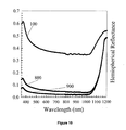
- Figure 10 shows reflectance measurements from two conditioned texture processes carried out at - 20° C (plot 800) and - 1° C (plot 900) temperatures. It is seen that lower temperature process gives rise to a significantly lower reflectance.
- Highly uniform texturing can be achieved by conditioning of the RIE chamber, and furthermore, this approach has the potential for being highly economical. For example, by conditioning a reaction chamber with metal coating, high throughput can be achieved since many etching runs can be completed without need for adding more metal. Eventually, the metal coating inside the chamber will degenerate, however, the potential exists for large amounts of Si to be textured in between down periods when reconditioning is done.
- etching of the textured Si surface in 40 % by weight of potassium hydroxide will remove damage without compromising the surface texture features.
- Other etchants for this purpose could include mixtures of hydrofluoric acid, nitric acid and acetic acid.
- damage may be removed by performing an isotropic plasma-less Si etch, i.e., using the vapor pressure from a XeF 2 crystal source, after the randomly distributed surface features have been generated.
- Figure 11 shows a comparison of internal quantum efficiency measurements relating to various treatments applied to remove damage.
- the Figure shows measurements for planar silicon (plot 444), untreated random RIE-textured silicon (plot 777) and KOH-etched treated RIE-textured Si solar cells (plot 666 showing results obtained using a 60-second treatment, and plot 555 showing results obtained using a 270-second treatment). It is apparent from these data that quantum efficiency improves by removal of surface damage using KOH. Removal of surface damage, however, is considered an optional step for purposes of the present invention, and it is noted that favorable results can be obtained even when the damage-removal etch is not performed.
Landscapes
- Photovoltaic Devices (AREA)
- Catalysts (AREA)
- Drying Of Semiconductors (AREA)
Claims (6)
- Procédé de formation d'une surface texturée (6) sur un substrat (4) en générant des caractéristiques de surface réparties de manière aléatoire sur celui-ci, le procédé comprenant l'étape consistant à exposer une surface du substrat (4) à un plasma de gravure par ions réactifs comprenant au moins un agent de gravure et des particules de métal introduites dans le plasma à des quantités qui ne sont pas à l'état de traces, depuis au moins une source, caractérisé en ce que les particules de métal comprennent un métal sélectionné parmi le groupe constitué de Cr, Au, Cu, Pd et Ti et de leurs combinaisons.
- Procédé selon la revendication 1, comprenant en outre l'étape consistant à exécuter une deuxième gravure après que les caractéristiques de surface réparties de manière aléatoire ont été générées, la deuxième gravure étant exécutée en utilisant un agent de gravure sélectionné à partir du groupe constitué de : KOH, un mélange d'acide nitrique et d'acide fluorhydrique, un mélange d'acide nitrique, d'acide fluorhydrique et d'acide acétique, et de la vapeur de fluorure de xénon.
- Procédé selon la revendication 1, dans lequel la gravure par ions réactifs est exécutée en utilisant une puissance HF d'environ 300 W, le temps de gravure est d'environ 15 minutes, les gaz de gravure utilisés comprennent du SF6 à un débit d'environ 14 sccm et de l'O2 à un débit d'environ 16 sccm, et la pression de chambre est d'environ 170 mT.
- Procédé de formation d'une pile solaire au silicium comprenant une surface texturée médiée par un catalyseur métallique (6), le procédé comprenant les étapes consistant à placer un matériau comprenant du silicium (4), lequel matériau comprend une surface, à l'intérieur d'une chambre de gravure par ions réactifs, introduire une source de métal en quantités qui ne sont pas à l'état de traces dans la chambre de gravure par ions réactifs, et exécuter une gravure par ions réactifs du matériau à l'intérieur de la chambre, grâce à quoi : un nuage de plasma est formé à l'intérieur de la chambre et, en raison de la présence de la source de métal à l'intérieur de la chambre de gravure par ions réactifs, des particules de métal provenant de ladite source de métal en viennent à être en suspension au moins temporairement dans le nuage de plasma, caractérisé en ce que les particules de métal comprennent un métal sélectionné à partir du groupe constitué de Cr, Au, Cu, Pd, et Ti et de leurs combinaisons.
- Procédé selon la revendication 4, comprenant en outre l'étape consistant à exécuter une deuxième gravure après que la surface texturée (6) a été générée, la deuxième gravure étant exécutée en utilisant un agent de gravure sélectionné à partir du groupe constitué de : KOH, un mélange d'acide nitrique et d'acide fluorhydrique, un mélange d'acide nitrique, d'acide fluorhydrique et d'acide acétique, et de la vapeur de fluorure de xénon.
- Procédé selon la revendication 1, caractérisé en ce que le substrat est sélectionné à partir du groupe constitué de semiconducteurs, de diélectriques, de verre et du silicium.
Applications Claiming Priority (3)
| Application Number | Priority Date | Filing Date | Title |
|---|---|---|---|
| US634905 | 1990-12-27 | ||
| US09/634,905 US6329296B1 (en) | 2000-08-09 | 2000-08-09 | Metal catalyst technique for texturing silicon solar cells |
| PCT/US2001/024340 WO2002013279A2 (fr) | 2000-08-09 | 2001-08-03 | Technique de catalyseur metallique pour texturer des piles solaires au silicium |
Publications (2)
| Publication Number | Publication Date |
|---|---|
| EP1316115A2 EP1316115A2 (fr) | 2003-06-04 |
| EP1316115B1 true EP1316115B1 (fr) | 2008-04-23 |
Family
ID=24545629
Family Applications (1)
| Application Number | Title | Priority Date | Filing Date |
|---|---|---|---|
| EP01955043A Expired - Lifetime EP1316115B1 (fr) | 2000-08-09 | 2001-08-03 | Technique de catalyseur metallique pour texturer des piles solaires au silicium |
Country Status (7)
| Country | Link |
|---|---|
| US (1) | US6329296B1 (fr) |
| EP (1) | EP1316115B1 (fr) |
| JP (1) | JP3855105B2 (fr) |
| AT (1) | ATE393479T1 (fr) |
| AU (1) | AU2001277250A1 (fr) |
| DE (1) | DE60133749D1 (fr) |
| WO (1) | WO2002013279A2 (fr) |
Cited By (1)
| Publication number | Priority date | Publication date | Assignee | Title |
|---|---|---|---|---|
| CN110729379A (zh) * | 2019-10-16 | 2020-01-24 | 哈尔滨工业大学 | 一种具有超低反射率微纳复合结构的黑硅衬底制备方法 |
Families Citing this family (31)
| Publication number | Priority date | Publication date | Assignee | Title |
|---|---|---|---|---|
| US7193128B2 (en) * | 1997-06-03 | 2007-03-20 | Chromatin, Inc. | Methods for generating or increasing revenues from crops |
| US6897085B2 (en) | 2003-01-21 | 2005-05-24 | Spheral Solar Power, Inc. | Method of fabricating an optical concentrator for a photovoltaic solar cell |
| US20060185715A1 (en) * | 2003-07-25 | 2006-08-24 | Hammerbacher Milfred D | Photovoltaic apparatus including spherical semiconducting particles |
| US20050148198A1 (en) * | 2004-01-05 | 2005-07-07 | Technion Research & Development Foundation Ltd. | Texturing a semiconductor material using negative potential dissolution (NPD) |
| US7563722B2 (en) * | 2004-03-05 | 2009-07-21 | Applied Nanotech Holdings, Inc. | Method of making a textured surface |
| DE102005048366A1 (de) * | 2005-10-10 | 2007-04-19 | X-Fab Semiconductor Foundries Ag | Verfahren zur Herstellung von defektarmen selbstorganisierten nadelartigen Strukturen mit Nano-Dimensionen im Bereich unterhalb der üblichen Lichtwellenlängen mit großem Aspektverhältnis |
| DE102005048361B4 (de) * | 2005-10-10 | 2011-07-14 | X-FAB Semiconductor Foundries AG, 99097 | Verfahren zur lokalen Beschichtung von Halbleiterschaltungen und diskreten Bauelementen mit einer thermischen SiO2-Schicht, deren Oberflächen Gebiete mit nadelförmigen Strukturen in Nanometerdimensionen enthalten |
| US8350209B2 (en) * | 2005-10-10 | 2013-01-08 | X-Fab Semiconductor Foundries Ag | Production of self-organized pin-type nanostructures, and the rather extensive applications thereof |
| JP4852972B2 (ja) * | 2005-10-26 | 2012-01-11 | パナソニック電工株式会社 | 光学部品の製造方法及び発光素子 |
| DE102006013670A1 (de) * | 2006-03-24 | 2007-09-27 | X-Fab Semiconductor Foundries Ag | Breitbandig entspiegelte optische Bauteile mit gekrümmten Oberflächen |
| DE102006046131B4 (de) | 2006-09-28 | 2020-06-25 | X-Fab Semiconductor Foundries Ag | Verfahren zur Herstellung einer optischen Schnittstelle für integrierte Optikanwendungen |
| DE102007024478A1 (de) * | 2007-05-25 | 2008-11-27 | Friedrich-Schiller-Universität Jena | Fotoempfindliches Halbleiterbauelement |
| KR100971658B1 (ko) * | 2008-01-03 | 2010-07-22 | 엘지전자 주식회사 | 실리콘 태양전지의 텍스처링 방법 |
| US20090236317A1 (en) * | 2008-03-21 | 2009-09-24 | Midwest Research Institute | Anti-reflection etching of silicon surfaces catalyzed with ionic metal solutions |
| US8075792B1 (en) * | 2008-03-21 | 2011-12-13 | Alliance For Sustainable Energy, Llc | Nanoparticle-based etching of silicon surfaces |
| US8815104B2 (en) * | 2008-03-21 | 2014-08-26 | Alliance For Sustainable Energy, Llc | Copper-assisted, anti-reflection etching of silicon surfaces |
| US8729798B2 (en) | 2008-03-21 | 2014-05-20 | Alliance For Sustainable Energy, Llc | Anti-reflective nanoporous silicon for efficient hydrogen production |
| KR20120003859A (ko) | 2009-03-17 | 2012-01-11 | 아이엠이씨 | 플라즈마 텍스처링 방법 |
| TWI379430B (en) * | 2009-04-16 | 2012-12-11 | Atomic Energy Council | A method of fabricating a thin interface for internal light reflection and impurities isolation |
| CA2815754A1 (fr) | 2009-11-11 | 2011-05-19 | Alliance For Sustainable Energy, Llc | Systemes et procedes chimiques par voie humide de production de substrats de silicium noir |
| US8828765B2 (en) | 2010-06-09 | 2014-09-09 | Alliance For Sustainable Energy, Llc | Forming high efficiency silicon solar cells using density-graded anti-reflection surfaces |
| WO2012061266A2 (fr) | 2010-11-01 | 2012-05-10 | The Board Of Trustees Of The University Of Illinois | Procédé de fabrication d'un réseau de nanostructures |
| CN104992990B (zh) * | 2010-12-30 | 2018-05-11 | 深圳市石金科技股份有限公司 | 一种降低硅片表面光反射率的方法 |
| US9276153B2 (en) | 2011-01-26 | 2016-03-01 | Sumco Corporation | Solar cell wafer and method of producing the same |
| CA2815764A1 (fr) | 2011-03-08 | 2012-09-13 | Alliance For Sustainable Energy, Llc | Dispositifs photovoltaiques au silicium noir efficaces ayant une meilleure reponse dans le bleu |
| JP2012246216A (ja) * | 2011-05-25 | 2012-12-13 | Agency For Science Technology & Research | 基板上にナノ構造を形成させる方法及びその使用 |
| TWI453927B (zh) | 2011-06-29 | 2014-09-21 | Ind Tech Res Inst | 多重反射結構以及光電元件 |
| WO2015069227A1 (fr) * | 2013-11-05 | 2015-05-14 | The Regents Of The University Of California | Mousse hybride à base de graphène et de nanotube de carbone à ancrage d'oxyde métallique |
| CN104393114A (zh) * | 2014-11-17 | 2015-03-04 | 中国电子科技集团公司第四十八研究所 | 一种微纳复合绒面结构的多晶黑硅制备方法 |
| CN106711240B (zh) * | 2016-11-14 | 2018-06-05 | 华南师范大学 | 一种半透明太阳能电池的制备方法 |
| CN109103301B (zh) * | 2018-08-30 | 2020-07-07 | 鲁东大学 | 一种多晶硅表面微纳复合结构的制备方法 |
Family Cites Families (3)
| Publication number | Priority date | Publication date | Assignee | Title |
|---|---|---|---|---|
| US4229233A (en) * | 1979-02-05 | 1980-10-21 | International Business Machines Corporation | Method for fabricating non-reflective semiconductor surfaces by anisotropic reactive ion etching |
| US4478209A (en) * | 1982-06-30 | 1984-10-23 | Guarnieri C Richard | Radiant energy collector having plasma-textured polyimide exposed surface |
| JP2000022185A (ja) * | 1998-07-03 | 2000-01-21 | Sharp Corp | 太陽電池セル及びその製造方法 |
-
2000
- 2000-08-09 US US09/634,905 patent/US6329296B1/en not_active Expired - Lifetime
-
2001
- 2001-08-03 JP JP2002518537A patent/JP3855105B2/ja not_active Expired - Lifetime
- 2001-08-03 AT AT01955043T patent/ATE393479T1/de not_active IP Right Cessation
- 2001-08-03 AU AU2001277250A patent/AU2001277250A1/en not_active Abandoned
- 2001-08-03 DE DE60133749T patent/DE60133749D1/de not_active Expired - Lifetime
- 2001-08-03 EP EP01955043A patent/EP1316115B1/fr not_active Expired - Lifetime
- 2001-08-03 WO PCT/US2001/024340 patent/WO2002013279A2/fr not_active Ceased
Non-Patent Citations (1)
| Title |
|---|
| H. JANSEN ET AL.: "RIE lag in high aspect ratio trench etching of silicon", MICROELECTRONIC ENGINEERING, vol. 35, February 1997 (1997-02-01), Amsterdam, NL, pages 45 - 50 * |
Cited By (2)
| Publication number | Priority date | Publication date | Assignee | Title |
|---|---|---|---|---|
| CN110729379A (zh) * | 2019-10-16 | 2020-01-24 | 哈尔滨工业大学 | 一种具有超低反射率微纳复合结构的黑硅衬底制备方法 |
| CN110729379B (zh) * | 2019-10-16 | 2021-05-04 | 哈尔滨工业大学 | 一种具有超低反射率微纳复合结构的黑硅衬底制备方法 |
Also Published As
| Publication number | Publication date |
|---|---|
| WO2002013279A2 (fr) | 2002-02-14 |
| ATE393479T1 (de) | 2008-05-15 |
| JP2004506330A (ja) | 2004-02-26 |
| US6329296B1 (en) | 2001-12-11 |
| EP1316115A2 (fr) | 2003-06-04 |
| AU2001277250A1 (en) | 2002-02-18 |
| DE60133749D1 (de) | 2008-06-05 |
| WO2002013279A3 (fr) | 2003-04-03 |
| JP3855105B2 (ja) | 2006-12-06 |
Similar Documents
| Publication | Publication Date | Title |
|---|---|---|
| EP1316115B1 (fr) | Technique de catalyseur metallique pour texturer des piles solaires au silicium | |
| Moreno et al. | Plasma texturing for silicon solar cells: From pyramids to inverted pyramids-like structures | |
| US8329046B2 (en) | Methods for damage etch and texturing of silicon single crystal substrates | |
| US20250033955A1 (en) | Formation of antireflective surfaces | |
| JP2022545188A (ja) | ペロブスカイト/シリコンタンデム型光起電力デバイス | |
| JP2013503476A (ja) | 太陽電池およびこのような太陽電池の製造方法 | |
| US8101522B2 (en) | Silicon substrate having nanostructures and method for producing the same and application thereof | |
| WO2010105703A1 (fr) | Procédé de texturage au plasma | |
| US20130306148A1 (en) | Method for fabricating substrate for solar cell and solar cell | |
| Kumaravelu et al. | Surface texturing for silicon solar cells using reactive ion etching technique | |
| US20230261124A1 (en) | High absorption photovoltaic material and methods of making the same | |
| US20180067235A1 (en) | Structured antireflection optical surface having a long lifetime and its manufacturing method | |
| Zhang et al. | Fabrication of ultra-low antireflection SiNWs arrays from mc-Si using one step MACE | |
| Costa et al. | Improving light capture on crystalline silicon wafers | |
| CN101624266B (zh) | 玻璃纹理化 | |
| Borra et al. | Development of a selective wet-chemical etchant for precise 3D sculpting of silicon enabled by infrared non-linear laser modification | |
| CN119452759A (zh) | 带纹理表面的生成、串联太阳能电池的制造以及串联太阳能电池 | |
| TW201140681A (en) | Texturing and damage etch of silicon single crystal (100) substrates | |
| Joshi et al. | Black silicon photovoltaics: fabrication methods and properties | |
| Blattmann et al. | Hybrid laser-etching-process for wafer texturing | |
| KR102514017B1 (ko) | 태양전지 기판의 습식 텍스쳐링 방법 | |
| Mohd Rais et al. | The impact of pulsed Nd: YAG laser on the surface of n-Si and photo-electrical performance of silicon solar cells | |
| Kim et al. | Reducing the optical reflectance of kerf-loss free silicon wafers via auto-masked CF4/O2 plasma etch | |
| Boudia et al. | Morphological and Optical Properties of Silicon Micro-nanostructures Induced by DC Corona Discharge at Atmospheric Pressure | |
| Sarkar et al. | Vertically aligned silicon nanowire arrays prepared by silver assisted single step chemical etching |
Legal Events
| Date | Code | Title | Description |
|---|---|---|---|
| PUAI | Public reference made under article 153(3) epc to a published international application that has entered the european phase |
Free format text: ORIGINAL CODE: 0009012 |
|
| AK | Designated contracting states |
Designated state(s): AT BE CH CY DE DK ES FI FR GB GR IE IT LI LU MC NL PT SE TR |
|
| AX | Request for extension of the european patent |
Extension state: AL LT LV MK RO SI |
|
| RIN1 | Information on inventor provided before grant (corrected) |
Inventor name: ZAIDI, SALEEM, HUSSAIN Inventor name: RUBY, DOUGLAS, S. |
|
| 17P | Request for examination filed |
Effective date: 20031006 |
|
| 17Q | First examination report despatched |
Effective date: 20060330 |
|
| GRAP | Despatch of communication of intention to grant a patent |
Free format text: ORIGINAL CODE: EPIDOSNIGR1 |
|
| GRAS | Grant fee paid |
Free format text: ORIGINAL CODE: EPIDOSNIGR3 |
|
| GRAA | (expected) grant |
Free format text: ORIGINAL CODE: 0009210 |
|
| AK | Designated contracting states |
Kind code of ref document: B1 Designated state(s): AT BE CH CY DE DK ES FI FR GB GR IE IT LI LU MC NL PT SE TR |
|
| REG | Reference to a national code |
Ref country code: GB Ref legal event code: FG4D |
|
| REG | Reference to a national code |
Ref country code: CH Ref legal event code: EP |
|
| REF | Corresponds to: |
Ref document number: 60133749 Country of ref document: DE Date of ref document: 20080605 Kind code of ref document: P |
|
| REG | Reference to a national code |
Ref country code: IE Ref legal event code: FG4D Free format text: LANGUAGE OF EP DOCUMENT: FRENCH |
|
| NLV1 | Nl: lapsed or annulled due to failure to fulfill the requirements of art. 29p and 29m of the patents act | ||
| PG25 | Lapsed in a contracting state [announced via postgrant information from national office to epo] |
Ref country code: ES Free format text: LAPSE BECAUSE OF FAILURE TO SUBMIT A TRANSLATION OF THE DESCRIPTION OR TO PAY THE FEE WITHIN THE PRESCRIBED TIME-LIMIT Effective date: 20080803 Ref country code: PT Free format text: LAPSE BECAUSE OF FAILURE TO SUBMIT A TRANSLATION OF THE DESCRIPTION OR TO PAY THE FEE WITHIN THE PRESCRIBED TIME-LIMIT Effective date: 20080923 Ref country code: NL Free format text: LAPSE BECAUSE OF FAILURE TO SUBMIT A TRANSLATION OF THE DESCRIPTION OR TO PAY THE FEE WITHIN THE PRESCRIBED TIME-LIMIT Effective date: 20080423 Ref country code: FI Free format text: LAPSE BECAUSE OF FAILURE TO SUBMIT A TRANSLATION OF THE DESCRIPTION OR TO PAY THE FEE WITHIN THE PRESCRIBED TIME-LIMIT Effective date: 20080423 |
|
| PG25 | Lapsed in a contracting state [announced via postgrant information from national office to epo] |
Ref country code: AT Free format text: LAPSE BECAUSE OF FAILURE TO SUBMIT A TRANSLATION OF THE DESCRIPTION OR TO PAY THE FEE WITHIN THE PRESCRIBED TIME-LIMIT Effective date: 20080423 |
|
| PG25 | Lapsed in a contracting state [announced via postgrant information from national office to epo] |
Ref country code: DK Free format text: LAPSE BECAUSE OF FAILURE TO SUBMIT A TRANSLATION OF THE DESCRIPTION OR TO PAY THE FEE WITHIN THE PRESCRIBED TIME-LIMIT Effective date: 20080423 Ref country code: SE Free format text: LAPSE BECAUSE OF FAILURE TO SUBMIT A TRANSLATION OF THE DESCRIPTION OR TO PAY THE FEE WITHIN THE PRESCRIBED TIME-LIMIT Effective date: 20080723 |
|
| EN | Fr: translation not filed | ||
| PG25 | Lapsed in a contracting state [announced via postgrant information from national office to epo] |
Ref country code: BE Free format text: LAPSE BECAUSE OF FAILURE TO SUBMIT A TRANSLATION OF THE DESCRIPTION OR TO PAY THE FEE WITHIN THE PRESCRIBED TIME-LIMIT Effective date: 20080423 |
|
| PLBE | No opposition filed within time limit |
Free format text: ORIGINAL CODE: 0009261 |
|
| STAA | Information on the status of an ep patent application or granted ep patent |
Free format text: STATUS: NO OPPOSITION FILED WITHIN TIME LIMIT |
|
| PG25 | Lapsed in a contracting state [announced via postgrant information from national office to epo] |
Ref country code: MC Free format text: LAPSE BECAUSE OF NON-PAYMENT OF DUE FEES Effective date: 20080831 |
|
| REG | Reference to a national code |
Ref country code: CH Ref legal event code: PL |
|
| 26N | No opposition filed |
Effective date: 20090126 |
|
| GBPC | Gb: european patent ceased through non-payment of renewal fee |
Effective date: 20080803 |
|
| PG25 | Lapsed in a contracting state [announced via postgrant information from national office to epo] |
Ref country code: DE Free format text: LAPSE BECAUSE OF FAILURE TO SUBMIT A TRANSLATION OF THE DESCRIPTION OR TO PAY THE FEE WITHIN THE PRESCRIBED TIME-LIMIT Effective date: 20080724 |
|
| REG | Reference to a national code |
Ref country code: IE Ref legal event code: MM4A |
|
| PG25 | Lapsed in a contracting state [announced via postgrant information from national office to epo] |
Ref country code: CH Free format text: LAPSE BECAUSE OF NON-PAYMENT OF DUE FEES Effective date: 20080831 Ref country code: LI Free format text: LAPSE BECAUSE OF NON-PAYMENT OF DUE FEES Effective date: 20080831 |
|
| PG25 | Lapsed in a contracting state [announced via postgrant information from national office to epo] |
Ref country code: IE Free format text: LAPSE BECAUSE OF NON-PAYMENT OF DUE FEES Effective date: 20080803 |
|
| PG25 | Lapsed in a contracting state [announced via postgrant information from national office to epo] |
Ref country code: IT Free format text: LAPSE BECAUSE OF FAILURE TO SUBMIT A TRANSLATION OF THE DESCRIPTION OR TO PAY THE FEE WITHIN THE PRESCRIBED TIME-LIMIT Effective date: 20080423 |
|
| PG25 | Lapsed in a contracting state [announced via postgrant information from national office to epo] |
Ref country code: GB Free format text: LAPSE BECAUSE OF NON-PAYMENT OF DUE FEES Effective date: 20080803 |
|
| PG25 | Lapsed in a contracting state [announced via postgrant information from national office to epo] |
Ref country code: CY Free format text: LAPSE BECAUSE OF FAILURE TO SUBMIT A TRANSLATION OF THE DESCRIPTION OR TO PAY THE FEE WITHIN THE PRESCRIBED TIME-LIMIT Effective date: 20080423 Ref country code: LU Free format text: LAPSE BECAUSE OF NON-PAYMENT OF DUE FEES Effective date: 20080803 |
|
| PG25 | Lapsed in a contracting state [announced via postgrant information from national office to epo] |
Ref country code: TR Free format text: LAPSE BECAUSE OF FAILURE TO SUBMIT A TRANSLATION OF THE DESCRIPTION OR TO PAY THE FEE WITHIN THE PRESCRIBED TIME-LIMIT Effective date: 20080423 |
|
| PG25 | Lapsed in a contracting state [announced via postgrant information from national office to epo] |
Ref country code: GR Free format text: LAPSE BECAUSE OF FAILURE TO SUBMIT A TRANSLATION OF THE DESCRIPTION OR TO PAY THE FEE WITHIN THE PRESCRIBED TIME-LIMIT Effective date: 20080724 |
|
| PG25 | Lapsed in a contracting state [announced via postgrant information from national office to epo] |
Ref country code: FR Free format text: LAPSE BECAUSE OF FAILURE TO SUBMIT A TRANSLATION OF THE DESCRIPTION OR TO PAY THE FEE WITHIN THE PRESCRIBED TIME-LIMIT Effective date: 20090227 |