EP1318541A2 - Arrangement des segments d'un masque et masque composé pour la préparation d'un dispositif à diodes électroluminescentes organiques - Google Patents
Arrangement des segments d'un masque et masque composé pour la préparation d'un dispositif à diodes électroluminescentes organiques Download PDFInfo
- Publication number
- EP1318541A2 EP1318541A2 EP02079966A EP02079966A EP1318541A2 EP 1318541 A2 EP1318541 A2 EP 1318541A2 EP 02079966 A EP02079966 A EP 02079966A EP 02079966 A EP02079966 A EP 02079966A EP 1318541 A2 EP1318541 A2 EP 1318541A2
- Authority
- EP
- European Patent Office
- Prior art keywords
- segments
- frame
- magnetic
- mask
- alignment
- Prior art date
- Legal status (The legal status is an assumption and is not a legal conclusion. Google has not performed a legal analysis and makes no representation as to the accuracy of the status listed.)
- Granted
Links
Images


Classifications
-
- C—CHEMISTRY; METALLURGY
- C23—COATING METALLIC MATERIAL; COATING MATERIAL WITH METALLIC MATERIAL; CHEMICAL SURFACE TREATMENT; DIFFUSION TREATMENT OF METALLIC MATERIAL; COATING BY VACUUM EVAPORATION, BY SPUTTERING, BY ION IMPLANTATION OR BY CHEMICAL VAPOUR DEPOSITION, IN GENERAL; INHIBITING CORROSION OF METALLIC MATERIAL OR INCRUSTATION IN GENERAL
- C23C—COATING METALLIC MATERIAL; COATING MATERIAL WITH METALLIC MATERIAL; SURFACE TREATMENT OF METALLIC MATERIAL BY DIFFUSION INTO THE SURFACE, BY CHEMICAL CONVERSION OR SUBSTITUTION; COATING BY VACUUM EVAPORATION, BY SPUTTERING, BY ION IMPLANTATION OR BY CHEMICAL VAPOUR DEPOSITION, IN GENERAL
- C23C14/00—Coating by vacuum evaporation, by sputtering or by ion implantation of the coating forming material
- C23C14/04—Coating on selected surface areas, e.g. using masks
- C23C14/042—Coating on selected surface areas, e.g. using masks using masks
-
- H—ELECTRICITY
- H10—SEMICONDUCTOR DEVICES; ELECTRIC SOLID-STATE DEVICES NOT OTHERWISE PROVIDED FOR
- H10P—GENERIC PROCESSES OR APPARATUS FOR THE MANUFACTURE OR TREATMENT OF DEVICES COVERED BY CLASS H10
- H10P76/00—Manufacture or treatment of masks on semiconductor bodies, e.g. by lithography or photolithography
-
- H—ELECTRICITY
- H10—SEMICONDUCTOR DEVICES; ELECTRIC SOLID-STATE DEVICES NOT OTHERWISE PROVIDED FOR
- H10K—ORGANIC ELECTRIC SOLID-STATE DEVICES
- H10K71/00—Manufacture or treatment specially adapted for the organic devices covered by this subclass
- H10K71/10—Deposition of organic active material
- H10K71/16—Deposition of organic active material using physical vapour deposition [PVD], e.g. vacuum deposition or sputtering
- H10K71/166—Deposition of organic active material using physical vapour deposition [PVD], e.g. vacuum deposition or sputtering using selective deposition, e.g. using a mask
-
- H—ELECTRICITY
- H10—SEMICONDUCTOR DEVICES; ELECTRIC SOLID-STATE DEVICES NOT OTHERWISE PROVIDED FOR
- H10K—ORGANIC ELECTRIC SOLID-STATE DEVICES
- H10K71/00—Manufacture or treatment specially adapted for the organic devices covered by this subclass
- H10K71/10—Deposition of organic active material
- H10K71/191—Deposition of organic active material characterised by provisions for the orientation or alignment of the layer to be deposited
-
- H—ELECTRICITY
- H10—SEMICONDUCTOR DEVICES; ELECTRIC SOLID-STATE DEVICES NOT OTHERWISE PROVIDED FOR
- H10P—GENERIC PROCESSES OR APPARATUS FOR THE MANUFACTURE OR TREATMENT OF DEVICES COVERED BY CLASS H10
- H10P72/00—Handling or holding of wafers, substrates or devices during manufacture or treatment thereof
- H10P72/50—Handling or holding of wafers, substrates or devices during manufacture or treatment thereof for positioning, orientation or alignment
- H10P72/57—Mask-wafer alignment
-
- H—ELECTRICITY
- H10—SEMICONDUCTOR DEVICES; ELECTRIC SOLID-STATE DEVICES NOT OTHERWISE PROVIDED FOR
- H10K—ORGANIC ELECTRIC SOLID-STATE DEVICES
- H10K71/00—Manufacture or treatment specially adapted for the organic devices covered by this subclass
Definitions
- the present invention relates to the deposition of organic material through a mask onto a substrate in the process of making an organic light emitting diode (OLED).
- OLED organic light emitting diode
- OLED organic light emitting devices
- the deposition mask is typically a precision mask made of a magnetic material and is thin and malleable.
- the deposition mask is lithographically patterned and because it is thin permits the appropriate thickness of organic material to be deposited on or over the substrate.
- the maximum size of a single piece depositions mask is limited by manufacturing process limitations, specifically dimensional accuracy and overall size. Another limitation of the present technology is the inability to replace damaged areas of the deposition mask.
- the deposition mask manufacturing process is subject to error and the increase in size and complexity of a mask design account for lower yield when manufacturing deposition masks. There is a need for more accurate, larger format precision deposition mask. There is also a need for a method of replacement of defective areas of the deposition mask.
- an alignment and holding device for permitting a deposition mask having a plurality of magnetic mask segments to be mounted to a frame for positioning relative to a substrate to facilitate simultaneous deposition of organic material on to the substrate which will be part of an organic light emitting device, comprising:
- the present invention makes possible the manufacture of a larger format deposition mask.
- An advantage of the present invention is that the deposition magnetic mask sections can be accurately assembled and mounted to a frame that is then positioned relative to the substrate. Magnetic mask segments can be held in place magnetically to make a mask assembly larger than is capable with single piece deposition mask. An assembled deposition mask can be disassembled to allow for removal of defective magnetic mask segments. The magnetic mask segments can then be replaced. An assembled deposition mask being made up of small segments are less expensive to produce. Assembled deposition masks have greater life expectancy, being repairable. An assembled deposition mask has greater accuracy than present single piece deposition masks (of similar size). This approach will improve yield and make possible deposition of larger substrates.
- FIG. 1 depicts an exploded view of an alignment device 10 for assembly and mounting of assembled magnetic mask segments 12a, 12b, 12c, 12d.
- On the deposition mask 12 there are four segments 12a, 12b, 12c, 12d (See FIG. 1 and FIG. 2).
- the mask segments are initially aligned with engraved alignment lines 19 on frame 22 when the disposition magnetic mask segments 12a, 12b, 12c, 12d are positioned.
- the alignment device 10 permits the deposition mask 12 to be positioned relative to a substrate of an OLED device to facilitate simultaneous deposition of organic material on to the substrate which will be part of an organic light emitting device.
- the alignment device 10 includes a base 14 having a first set of alignment pins 16 and a second set of alignment pins 18.
- the alignment pins 16 as shown include two pins disposed on opposite sides of the base 14.
- the base 14 is generally rectangular and the second set of alignment pins 18 are disposed in three corners of the base 14. As shown, in one of the corners there are two alignment pins 18a and 18b but in the remaining two corners there is a single alignment pin 18.
- a series of plate segments 20a, 20b, 20c, 20d are secured to the base 14 by any convenient means.
- the plate segments 20a, 20b, 20c, 20d are fastened by screws to the base 14. Although the screws are not shown for convenience of illustration are depicted by holes 15.
- the plate segments 20a, 20b, 20c, 20d provide a top flat surface on which the magnetic mask segments 12 are to be positioned.
- a frame 22, generally rectangular in shape, has central openings 24a, 24b, 24c, 24d.
- Cross bar receiving channels 30 are formed in the frame 22.
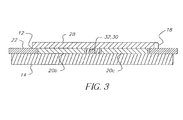
- a magnetic cross bar 32 having a plurality of magnets are disposed in the cross bar receiving channels 30 (see FIG. 3).
- Around each of the four corners of the frame 22 there are cutout segments 26. In three of the cutout segments 26, the alignment pins 18 project through (see FIG. 2.)
- cutout segments 26 The purpose of these cutout segments 26 is to facilitate positioning of the frame 22 in a vacuum chamber which permits the engagement of a mechanism in the vacuum chamber as well understood in the art.
- the frame 22 is removable and mounted to the base 14 using alignment pins 16.
- the alignment pins 16 pass through holes 17a and 17b in the frame 22.
- the hole 17a has a circular cross-section and hole 17b has an oblong shape to permit proper alignment.
- the deposition mask 12 includes segments 12a, 12b, 12c, and 12d are positioned on plate segments 20a, 20b, 20c, 20d and frame 22.
- a transparent flat plate 28 is positioned to contact the second set of alignment pins 18 and magnetic mask segments 12 and is sized to expose edge segments of the deposition mask 12 when it is properly positioned.
- the transparent flat plate 28 includes fiducial marks 21 and 27 which are electroplated.
- the fiducial marks 21 and 27 are cross lines which are shown larger than they actually are.
- the fiducial marks 21 and 27 are used to permit alignment with fiducial marks 23 and 29 on the magnetic mask segments 12.
- the alignment of fiducial marks 27 and 29 form an appropriate relationship between mask segments 12a, 12b, 12c, and 12d.
- the exposed segments of the deposition mask 12 are secured to the frame 22 by adhesive tape 25 which is in engagement with the magnetic mask segments 12a, 12 b, 12c and 12d and perimeter of frame 22.
- the magnetic mask segments 12a, 12 b, 12c and 12d are secured to the frame 22 by the magnetic attraction of the magnetic mask segments 12a, 12 b, 12c and 12d to the magnets of magnetic cross bar 32.
- the cross bar magnets can be adhesively bonded in magnetic cross bar receiving channels 30.
- FIGS. 2 and 3 respectively show a top view of the alignment device 10 and a cross-sectional view taken along lines 3-3.
- the base 14, plate segments 20a, 20b, 20c, 20d, the magnetic mask segments 12a, 12 b, 12c and 12d and the transparent flat plate 28 are shown stacked one on top of the other.
- the top surface of frame 22 is shown to be planar with plate segments 20a, 20b, 20c, 20d.
- One of the pins 18 is shown in its alignment position.
- the alignment of the magnetic mask segments 12a, 12 b, 12c and 12d in the alignment device 10 will now be described.
- the frame 22 is mounted on base 14 using alignment pins 16.
- the alignment pins 16 are located on the base 14 in such a manner that frame 22 can be mounted in one orientation only.
- the frame 22 when mounted on base 14 is to be positioned in a manner that aligns plate segments 20 top surface is at the same identical height as frame 22.
- the magnetic mask segments 12a, 12b, 12c, 12d are visually aligned on top of plates segments 20 and frame 22 using engraved alignment lines 19 on frame 22 for initial alignment as shown in FIG. 2.
- the transparent flat plate 28 is placed on top of deposition mask 12 and against alignment pins 18, 18a, and 18b.
- the magnetic mask segments 12a, 12b, 12c, 12d are manually aligned using the photo-etched fiducials 23 and 29 corresponding with fiducials 21 and 27 located on transparent flat plate 28.
- the relationship of transparent flat plate 28 and alignment pins 18, 18a, and 18b must remain against the alignment pins 18a and 18b during the alignment process. After alignment the deposition mask sections are held in place using clamp 31.
- the deposition mask 12 is then attached to frame 22 using two methods.
- adhesive tape 25 secure the deposition mask 12 to the perimeter of frame 22. Only one of the adhesive tape 25 is shown although typically there will be two for each edge and they secure the deposition mask 12 to the frame 22.
- the magnetic mask segments 12a, 12b, 12c and 12d are then held using a plurality of magnets to the frame cross bar 32.
- the term " cross bar” will be understood to mean one or more magnetic members which when positioned in the cross bar receiving channels 30 secures the magnetic mask segments 12a, 12b, 12c and 12d.
- the cross bar receiving channel 30 can extend along a single line segment rather than the two shown and receive one or more magnetic members.
- the magnetic cross bar 32 can include a single magnetic member made of a rubberized material and two shorter members on either side of the single member which completes the magnetic cross bar 32.
- the deposition mask 12 is made from magnetic material.
- the amount of ferrous metals is such that the field exerted by the magnets provide within the frame 22 causes the deposition mask 12 to be secured to the frame 22 and held in a planar fashion.
- the transparent flat plate 28 is removed.
- the assembled deposition mask 12 and frame 22 are removed from base 14. It is the assembled deposition mask 12 and frame 22 that are placed in a chamber (not shown).
Landscapes
- Chemical & Material Sciences (AREA)
- Engineering & Computer Science (AREA)
- Manufacturing & Machinery (AREA)
- Chemical Kinetics & Catalysis (AREA)
- Materials Engineering (AREA)
- Mechanical Engineering (AREA)
- Metallurgy (AREA)
- Organic Chemistry (AREA)
- Physical Vapour Deposition (AREA)
- Electroluminescent Light Sources (AREA)
Applications Claiming Priority (2)
| Application Number | Priority Date | Filing Date | Title |
|---|---|---|---|
| US16451 | 2001-12-10 | ||
| US10/016,451 US6749690B2 (en) | 2001-12-10 | 2001-12-10 | Aligning mask segments to provide an assembled mask for producing OLED devices |
Publications (3)
| Publication Number | Publication Date |
|---|---|
| EP1318541A2 true EP1318541A2 (fr) | 2003-06-11 |
| EP1318541A3 EP1318541A3 (fr) | 2004-12-15 |
| EP1318541B1 EP1318541B1 (fr) | 2006-12-27 |
Family
ID=21777188
Family Applications (1)
| Application Number | Title | Priority Date | Filing Date |
|---|---|---|---|
| EP02079966A Expired - Lifetime EP1318541B1 (fr) | 2001-12-10 | 2002-11-28 | Arrangement des segments d'un masque et masque composé pour la préparation d'un dispositif à diodes électroluminescentes organiques |
Country Status (7)
| Country | Link |
|---|---|
| US (1) | US6749690B2 (fr) |
| EP (1) | EP1318541B1 (fr) |
| JP (1) | JP4373076B2 (fr) |
| KR (1) | KR20030047825A (fr) |
| CN (1) | CN1279629C (fr) |
| DE (1) | DE60217056T2 (fr) |
| TW (1) | TW565742B (fr) |
Cited By (2)
| Publication number | Priority date | Publication date | Assignee | Title |
|---|---|---|---|---|
| WO2014093501A1 (fr) * | 2012-12-13 | 2014-06-19 | Varian Semiconductor Equipment Associates, Inc. | Système d'alignement de masque pour traitement de semiconducteur |
| CN111010877A (zh) * | 2018-08-06 | 2020-04-14 | 应用材料公司 | 具有掩模对准器的沉积设备、用于遮蔽基板的掩模布置和用于遮蔽基板的方法 |
Families Citing this family (56)
| Publication number | Priority date | Publication date | Assignee | Title |
|---|---|---|---|---|
| US7396558B2 (en) * | 2001-01-31 | 2008-07-08 | Toray Industries, Inc. | Integrated mask and method and apparatus for manufacturing organic EL device using the same |
| CN100464440C (zh) * | 2002-06-03 | 2009-02-25 | 三星移动显示器株式会社 | 用于有机电致发光装置的薄层真空蒸发的掩模框组件 |
| US20030221620A1 (en) * | 2002-06-03 | 2003-12-04 | Semiconductor Energy Laboratory Co., Ltd. | Vapor deposition device |
| KR100534580B1 (ko) * | 2003-03-27 | 2005-12-07 | 삼성에스디아이 주식회사 | 표시장치용 증착 마스크 및 그의 제조방법 |
| JP2005276480A (ja) * | 2004-03-23 | 2005-10-06 | Seiko Epson Corp | マスク、マスクの製造方法、薄膜パターンの形成方法、電気光学装置の製造方法および電子機器 |
| US20060086321A1 (en) * | 2004-10-22 | 2006-04-27 | Advantech Global, Ltd | Substrate-to-mask alignment and securing system with temperature control for use in an automated shadow mask vacuum deposition process |
| CN100529170C (zh) * | 2005-04-22 | 2009-08-19 | 鸿富锦精密工业(深圳)有限公司 | 基板载具 |
| KR20070082317A (ko) * | 2006-02-16 | 2007-08-21 | 삼성전자주식회사 | 마스크 및 그 제조 방법 |
| KR100753096B1 (ko) * | 2006-08-17 | 2007-08-31 | 삼성전기주식회사 | 정렬방법 및 이를 이용한 임프린팅 방법 |
| KR101266489B1 (ko) * | 2006-12-26 | 2013-05-23 | 삼성디스플레이 주식회사 | 쉐도우 마스크 장치 및 이를 이용한 유기 전계발광표시장치의 제조 방법 |
| CN101965634A (zh) * | 2008-01-25 | 2011-02-02 | 最高科研理事会 | 用于有选择地在微电子衬底上沉积薄膜的自对准的金属掩模组件以及使用方法 |
| US20090203283A1 (en) * | 2008-02-07 | 2009-08-13 | Margaret Helen Gentile | Method for sealing an electronic device |
| DE102008037387A1 (de) * | 2008-09-24 | 2010-03-25 | Aixtron Ag | Verfahren sowie Vorrichtung zum Abscheiden lateral strukturierter Schichten mittels einer magnetisch auf einem Substrathalter gehaltenen Schattenmaske |
| TWI398533B (zh) * | 2009-12-29 | 2013-06-11 | Au Optronics Corp | 蔭罩及其製作方法 |
| KR101182440B1 (ko) * | 2010-01-11 | 2012-09-12 | 삼성디스플레이 주식회사 | 박막 증착용 마스크 프레임 조립체 |
| KR101309864B1 (ko) * | 2010-02-02 | 2013-09-16 | 엘지디스플레이 주식회사 | 마스크 어셈블리 |
| KR101232181B1 (ko) * | 2010-02-03 | 2013-02-12 | 엘지디스플레이 주식회사 | 마스크 어셈블리 |
| CN102373419A (zh) * | 2010-08-23 | 2012-03-14 | 鸿富锦精密工业(深圳)有限公司 | 镀膜加工方法 |
| CN102373408A (zh) * | 2010-08-25 | 2012-03-14 | 鸿富锦精密工业(深圳)有限公司 | 镀膜加工方法 |
| CN103165828B (zh) * | 2011-12-16 | 2015-08-26 | 昆山工研院新型平板显示技术中心有限公司 | 荫罩及其制备方法 |
| CN103205681B (zh) * | 2012-01-16 | 2017-02-08 | 昆山允升吉光电科技有限公司 | 对位辅助板 |
| CN104685095B (zh) * | 2012-04-19 | 2017-12-29 | 因特瓦克公司 | 用于制造太阳能电池的双掩模装置 |
| EP2839522A4 (fr) * | 2012-04-20 | 2015-12-09 | Rensselaer Polytech Inst | Diodes électroluminescentes et procédé de conditionnement de celles-ci |
| US10062600B2 (en) | 2012-04-26 | 2018-08-28 | Intevac, Inc. | System and method for bi-facial processing of substrates |
| KR102072872B1 (ko) | 2012-04-26 | 2020-02-03 | 인테벡, 인코포레이티드 | 진공 처리용 시스템 아키텍처 |
| US9579680B2 (en) * | 2013-01-31 | 2017-02-28 | Wki Holding Company, Inc. | Self-centering magnetic masking system |
| KR102099238B1 (ko) * | 2013-05-13 | 2020-04-10 | 삼성디스플레이 주식회사 | 마스크 조립체 및 이를 이용한 박막 증착 방법 |
| US9490153B2 (en) | 2013-07-26 | 2016-11-08 | Varian Semiconductor Equipment Associates, Inc. | Mechanical alignment of substrates to a mask |
| US9333733B2 (en) * | 2013-07-26 | 2016-05-10 | Varian Semiconductor Equipment Associates, Inc. | Multi-part mask for implanting workpieces |
| US9053405B1 (en) * | 2013-08-27 | 2015-06-09 | Flextronics Ap, Llc | Printed RFID circuit |
| CN103762291B (zh) * | 2013-12-27 | 2016-05-18 | 铜陵中发三佳科技股份有限公司 | 适用于led支架emc封装的料片排料和投料装置 |
| CN103713466B (zh) * | 2013-12-30 | 2016-05-11 | 京东方科技集团股份有限公司 | 掩膜板及其制作方法 |
| US9627558B2 (en) * | 2014-04-09 | 2017-04-18 | Arizona Board Of Regents On Behalf Of Arizona State University | Methods and apparatuses for manufacturing self-aligned integrated back contact heterojunction solar cells |
| JP6607923B2 (ja) | 2014-08-05 | 2019-11-20 | インテヴァック インコーポレイテッド | 注入マスク及びアライメント |
| KR102280269B1 (ko) * | 2014-11-05 | 2021-07-22 | 삼성디스플레이 주식회사 | 마스크 프레임 조립체 및 그 제조 방법 |
| CN104746015B (zh) * | 2015-03-17 | 2017-10-27 | 京东方科技集团股份有限公司 | 面板对位调节装置及其对位方法 |
| CN104914679B (zh) * | 2015-05-18 | 2018-11-20 | 合肥芯硕半导体有限公司 | 一种用于半导体光刻的多功能高产能吸盘 |
| KR20170059068A (ko) | 2015-11-19 | 2017-05-30 | 삼성전자주식회사 | 광원 모듈, 디스플레이 패널 및 이를 구비한 디스플레이 장치 |
| CN105549320A (zh) * | 2016-01-05 | 2016-05-04 | 京东方科技集团股份有限公司 | 一种对位标记结构、掩模板、基板以及对位方法 |
| KR102505877B1 (ko) * | 2016-01-29 | 2023-03-06 | 삼성디스플레이 주식회사 | 마스크 프레임 조립체 및 이를 이용한 디스플레이 장치의 제조방법 |
| CN105887010B (zh) * | 2016-05-13 | 2018-10-26 | 京东方科技集团股份有限公司 | 掩膜集成框架及蒸镀设备 |
| CN106702318B (zh) * | 2016-12-12 | 2018-11-23 | 京东方科技集团股份有限公司 | 掩膜框架及制造方法和掩膜板 |
| CN106480404B (zh) * | 2016-12-28 | 2019-05-03 | 京东方科技集团股份有限公司 | 一种掩膜集成框架及蒸镀装置 |
| CN107099768B (zh) * | 2017-04-28 | 2019-07-12 | 东晶锐康晶体(成都)有限公司 | 一种石英晶体振荡器真空溅射镀膜掩膜板的校准装置及方法 |
| WO2019180846A1 (fr) * | 2018-03-20 | 2019-09-26 | シャープ株式会社 | Masque de formation de film et procédé de fabrication d'un dispositif d'affichage l'utilisant |
| CN110750031B (zh) * | 2018-07-23 | 2021-10-29 | 上海微电子装备(集团)股份有限公司 | 一种拼接式掩模版、曝光装置及曝光方法 |
| KR102631255B1 (ko) * | 2018-10-18 | 2024-01-31 | 삼성디스플레이 주식회사 | 하이브리드형 마스크 스틱과, 이를 적용한 마스크 프레임 어셈블리 |
| US11613802B2 (en) * | 2020-04-17 | 2023-03-28 | Rockwell Collins, Inc. | Additively manufactured shadow masks for material deposition control |
| CN111424234B (zh) * | 2020-05-09 | 2024-10-15 | 江苏集萃有机光电技术研究所有限公司 | 一种对位模块、对位设备、薄膜沉积生产线及控制方法 |
| CN111471960B (zh) * | 2020-06-09 | 2022-09-09 | 京东方科技集团股份有限公司 | 掩膜板以及制备方法 |
| US11715662B2 (en) * | 2020-12-11 | 2023-08-01 | Applied Materials, Inc. | Actively clamped carrier assembly for processing tools |
| US11781210B2 (en) * | 2021-03-09 | 2023-10-10 | Samsung Display Co., Ltd. | Magnet assembly and deposition apparatus including the same |
| KR102936519B1 (ko) * | 2021-11-08 | 2026-03-10 | 삼성디스플레이 주식회사 | 마스크 어셈블리 및 이의 수리방법 |
| KR20230096185A (ko) * | 2021-12-22 | 2023-06-30 | 삼성디스플레이 주식회사 | 마스크 어셈블리, 이의 수리방법, 및 이의 제조방법 |
| JP2023149070A (ja) * | 2022-03-30 | 2023-10-13 | 大日本印刷株式会社 | 蒸着システム及び蒸着方法 |
| CN115747715B (zh) * | 2022-11-30 | 2024-09-20 | 中国科学院上海技术物理研究所 | 支撑板、吸引体、掩膜块和掩膜版组件 |
Family Cites Families (5)
| Publication number | Priority date | Publication date | Assignee | Title |
|---|---|---|---|---|
| GB1484463A (en) * | 1975-01-28 | 1977-09-01 | Marconi Co Ltd | Method of aligning a protective mask |
| US4676193A (en) * | 1984-02-27 | 1987-06-30 | Applied Magnetics Corporation | Stabilized mask assembly for direct deposition of a thin film pattern onto a substrate |
| US6146489A (en) * | 1998-11-19 | 2000-11-14 | General Electric Company | Method and apparatus for depositing scintillator material on radiation imager |
| US6475287B1 (en) * | 2001-06-27 | 2002-11-05 | Eastman Kodak Company | Alignment device which facilitates deposition of organic material through a deposition mask |
| US6589382B2 (en) * | 2001-11-26 | 2003-07-08 | Eastman Kodak Company | Aligning mask segments to provide a stitched mask for producing OLED devices |
-
2001
- 2001-12-10 US US10/016,451 patent/US6749690B2/en not_active Expired - Lifetime
-
2002
- 2002-10-22 TW TW091124348A patent/TW565742B/zh not_active IP Right Cessation
- 2002-11-28 DE DE60217056T patent/DE60217056T2/de not_active Expired - Lifetime
- 2002-11-28 EP EP02079966A patent/EP1318541B1/fr not_active Expired - Lifetime
- 2002-12-09 JP JP2002356285A patent/JP4373076B2/ja not_active Expired - Lifetime
- 2002-12-09 KR KR1020020077786A patent/KR20030047825A/ko not_active Withdrawn
- 2002-12-10 CN CNB021540950A patent/CN1279629C/zh not_active Expired - Lifetime
Cited By (3)
| Publication number | Priority date | Publication date | Assignee | Title |
|---|---|---|---|---|
| WO2014093501A1 (fr) * | 2012-12-13 | 2014-06-19 | Varian Semiconductor Equipment Associates, Inc. | Système d'alignement de masque pour traitement de semiconducteur |
| US9570309B2 (en) | 2012-12-13 | 2017-02-14 | Varian Semiconductor Equipment Associates, Inc. | Mask alignment system for semiconductor processing |
| CN111010877A (zh) * | 2018-08-06 | 2020-04-14 | 应用材料公司 | 具有掩模对准器的沉积设备、用于遮蔽基板的掩模布置和用于遮蔽基板的方法 |
Also Published As
| Publication number | Publication date |
|---|---|
| TW565742B (en) | 2003-12-11 |
| EP1318541A3 (fr) | 2004-12-15 |
| DE60217056T2 (de) | 2007-08-09 |
| KR20030047825A (ko) | 2003-06-18 |
| US20030108805A1 (en) | 2003-06-12 |
| CN1424775A (zh) | 2003-06-18 |
| CN1279629C (zh) | 2006-10-11 |
| JP4373076B2 (ja) | 2009-11-25 |
| EP1318541B1 (fr) | 2006-12-27 |
| DE60217056D1 (de) | 2007-02-08 |
| US6749690B2 (en) | 2004-06-15 |
| JP2003249358A (ja) | 2003-09-05 |
Similar Documents
| Publication | Publication Date | Title |
|---|---|---|
| EP1318541B1 (fr) | Arrangement des segments d'un masque et masque composé pour la préparation d'un dispositif à diodes électroluminescentes organiques | |
| US6589382B2 (en) | Aligning mask segments to provide a stitched mask for producing OLED devices | |
| JP4216531B2 (ja) | アラインメントデバイス及び有機材料の蒸着方法 | |
| KR101122585B1 (ko) | 유기발광 표시장치의 제조방법 | |
| KR100811730B1 (ko) | 마스크막형성방법 및 마스크막형성장치 | |
| US4915057A (en) | Apparatus and method for registration of shadow masked thin-film patterns | |
| CN1732282A (zh) | 安装沉积掩模的柔性框 | |
| JPS6299782A (ja) | シヤドウマスクによる薄膜パタ−ンの整合装置及び方法 | |
| JP2002371349A (ja) | 蒸着用マスク | |
| KR101638344B1 (ko) | 스퍼터링용 원판패널 고정 장치 및 방법 | |
| JP7203888B2 (ja) | 支持装置 | |
| EP3690078B1 (fr) | Masque de dépôt en phase vapeur | |
| CN115928008B (zh) | 高精细掩膜板及其制造方法 | |
| JP3082805U (ja) | 蒸着用マスク | |
| JP2007138256A (ja) | 蒸着方法 | |
| JP2004126360A (ja) | マイクロレンズアレイとその製法 | |
| CN117377372B (zh) | 微细结构加工治具及微细图形加工方法 | |
| JP4131096B2 (ja) | 回路基板の製造方法 | |
| JP2003121676A (ja) | 光ファイバアレイ、光ファイバ位置決め方法及び光ファイバ位置決め板 | |
| CN210261956U (zh) | Oled蒸镀掩模板 | |
| JP2006294280A (ja) | 蒸着膜の形成方法および蒸着装置、並びに有機発光ディスプレイの製造方法 | |
| CN110249071A (zh) | 蒸镀掩模固定装置 | |
| JP2004246267A (ja) | 光部品実装構造とその製法 | |
| JP2008015544A (ja) | 光部品実装構造 |
Legal Events
| Date | Code | Title | Description |
|---|---|---|---|
| PUAI | Public reference made under article 153(3) epc to a published international application that has entered the european phase |
Free format text: ORIGINAL CODE: 0009012 |
|
| AK | Designated contracting states |
Designated state(s): AT BE BG CH CY CZ DE DK EE ES FI FR GB GR IE IT LI LU MC NL PT SE SK TR |
|
| AX | Request for extension of the european patent |
Extension state: AL LT LV MK RO SI |
|
| PUAL | Search report despatched |
Free format text: ORIGINAL CODE: 0009013 |
|
| AK | Designated contracting states |
Kind code of ref document: A3 Designated state(s): AT BE BG CH CY CZ DE DK EE ES FI FR GB GR IE IT LI LU MC NL PT SE SK TR |
|
| AX | Request for extension of the european patent |
Extension state: AL LT LV MK RO SI |
|
| RIC1 | Information provided on ipc code assigned before grant |
Ipc: 7H 01L 21/68 B Ipc: 7H 01L 21/00 A Ipc: 7G 03F 7/20 B |
|
| 17P | Request for examination filed |
Effective date: 20050523 |
|
| AKX | Designation fees paid |
Designated state(s): DE FR GB |
|
| GRAP | Despatch of communication of intention to grant a patent |
Free format text: ORIGINAL CODE: EPIDOSNIGR1 |
|
| RIN1 | Information on inventor provided before grant (corrected) |
Inventor name: CLARK, THOMAS, KENYON,EASTMAN KODAK COMPANY |
|
| GRAS | Grant fee paid |
Free format text: ORIGINAL CODE: EPIDOSNIGR3 |
|
| GRAA | (expected) grant |
Free format text: ORIGINAL CODE: 0009210 |
|
| AK | Designated contracting states |
Kind code of ref document: B1 Designated state(s): DE FR GB |
|
| REG | Reference to a national code |
Ref country code: GB Ref legal event code: FG4D |
|
| REF | Corresponds to: |
Ref document number: 60217056 Country of ref document: DE Date of ref document: 20070208 Kind code of ref document: P |
|
| ET | Fr: translation filed | ||
| PLBE | No opposition filed within time limit |
Free format text: ORIGINAL CODE: 0009261 |
|
| STAA | Information on the status of an ep patent application or granted ep patent |
Free format text: STATUS: NO OPPOSITION FILED WITHIN TIME LIMIT |
|
| 26N | No opposition filed |
Effective date: 20070928 |
|
| REG | Reference to a national code |
Ref country code: FR Ref legal event code: TP |
|
| REG | Reference to a national code |
Ref country code: GB Ref legal event code: 732E Free format text: REGISTERED BETWEEN 20110224 AND 20110302 |
|
| REG | Reference to a national code |
Ref country code: FR Ref legal event code: PLFP Year of fee payment: 14 |
|
| REG | Reference to a national code |
Ref country code: FR Ref legal event code: PLFP Year of fee payment: 15 |
|
| REG | Reference to a national code |
Ref country code: FR Ref legal event code: PLFP Year of fee payment: 16 |
|
| PGFP | Annual fee paid to national office [announced via postgrant information from national office to epo] |
Ref country code: DE Payment date: 20211118 Year of fee payment: 20 Ref country code: FR Payment date: 20211119 Year of fee payment: 20 Ref country code: GB Payment date: 20211118 Year of fee payment: 20 |
|
| REG | Reference to a national code |
Ref country code: DE Ref legal event code: R071 Ref document number: 60217056 Country of ref document: DE |
|
| REG | Reference to a national code |
Ref country code: GB Ref legal event code: PE20 Expiry date: 20221127 |
|
| PG25 | Lapsed in a contracting state [announced via postgrant information from national office to epo] |
Ref country code: GB Free format text: LAPSE BECAUSE OF EXPIRATION OF PROTECTION Effective date: 20221127 |