EP1321784A2 - Connecteur d'ensemble de fibres optiques et procédé de fabrication de marques d'ajustage - Google Patents
Connecteur d'ensemble de fibres optiques et procédé de fabrication de marques d'ajustage Download PDFInfo
- Publication number
- EP1321784A2 EP1321784A2 EP02080197A EP02080197A EP1321784A2 EP 1321784 A2 EP1321784 A2 EP 1321784A2 EP 02080197 A EP02080197 A EP 02080197A EP 02080197 A EP02080197 A EP 02080197A EP 1321784 A2 EP1321784 A2 EP 1321784A2
- Authority
- EP
- European Patent Office
- Prior art keywords
- fiber optic
- optical
- fiducial marks
- array
- optic array
- Prior art date
- Legal status (The legal status is an assumption and is not a legal conclusion. Google has not performed a legal analysis and makes no representation as to the accuracy of the status listed.)
- Withdrawn
Links
- 239000000835 fiber Substances 0.000 title claims abstract description 65
- 238000004519 manufacturing process Methods 0.000 title claims abstract description 25
- 230000003287 optical effect Effects 0.000 claims abstract description 119
- 238000000034 method Methods 0.000 claims description 28
- 238000003491 array Methods 0.000 description 10
- 239000000463 material Substances 0.000 description 10
- 239000004065 semiconductor Substances 0.000 description 10
- 239000000758 substrate Substances 0.000 description 6
- 235000012431 wafers Nutrition 0.000 description 4
- 229910003460 diamond Inorganic materials 0.000 description 3
- 239000010432 diamond Substances 0.000 description 3
- 238000007516 diamond turning Methods 0.000 description 3
- 238000003801 milling Methods 0.000 description 3
- 238000000465 moulding Methods 0.000 description 3
- 239000000853 adhesive Substances 0.000 description 2
- 230000001070 adhesive effect Effects 0.000 description 2
- 230000015572 biosynthetic process Effects 0.000 description 2
- 238000003618 dip coating Methods 0.000 description 2
- 238000007373 indentation Methods 0.000 description 2
- 238000005259 measurement Methods 0.000 description 2
- KJLLKLRVCJAFRY-UHFFFAOYSA-N mebutizide Chemical compound ClC1=C(S(N)(=O)=O)C=C2S(=O)(=O)NC(C(C)C(C)CC)NC2=C1 KJLLKLRVCJAFRY-UHFFFAOYSA-N 0.000 description 2
- 238000007788 roughening Methods 0.000 description 2
- 238000004528 spin coating Methods 0.000 description 2
- 238000001771 vacuum deposition Methods 0.000 description 2
- 239000006096 absorbing agent Substances 0.000 description 1
- 230000000052 comparative effect Effects 0.000 description 1
- 230000008878 coupling Effects 0.000 description 1
- 238000010168 coupling process Methods 0.000 description 1
- 238000005859 coupling reaction Methods 0.000 description 1
- 238000011161 development Methods 0.000 description 1
- 230000018109 developmental process Effects 0.000 description 1
- 230000000694 effects Effects 0.000 description 1
- 238000004049 embossing Methods 0.000 description 1
- 238000005530 etching Methods 0.000 description 1
- 238000003384 imaging method Methods 0.000 description 1
- 238000007641 inkjet printing Methods 0.000 description 1
- 239000004973 liquid crystal related substance Substances 0.000 description 1
- 238000010422 painting Methods 0.000 description 1
- 238000004382 potting Methods 0.000 description 1
- 238000007639 printing Methods 0.000 description 1
- 238000000926 separation method Methods 0.000 description 1
- 229910000679 solder Inorganic materials 0.000 description 1
- 238000007514 turning Methods 0.000 description 1
Images


Classifications
-
- G—PHYSICS
- G02—OPTICS
- G02B—OPTICAL ELEMENTS, SYSTEMS OR APPARATUS
- G02B3/00—Simple or compound lenses
- G02B3/0006—Arrays
- G02B3/0037—Arrays characterized by the distribution or form of lenses
- G02B3/005—Arrays characterized by the distribution or form of lenses arranged along a single direction only, e.g. lenticular sheets
-
- G—PHYSICS
- G02—OPTICS
- G02B—OPTICAL ELEMENTS, SYSTEMS OR APPARATUS
- G02B27/00—Optical systems or apparatus not provided for by any of the groups G02B1/00 - G02B26/00, G02B30/00
- G02B27/32—Fiducial marks and measuring scales within the optical system
-
- G—PHYSICS
- G02—OPTICS
- G02B—OPTICAL ELEMENTS, SYSTEMS OR APPARATUS
- G02B3/00—Simple or compound lenses
- G02B3/0006—Arrays
- G02B3/0012—Arrays characterised by the manufacturing method
-
- G—PHYSICS
- G02—OPTICS
- G02B—OPTICAL ELEMENTS, SYSTEMS OR APPARATUS
- G02B3/00—Simple or compound lenses
- G02B3/0006—Arrays
- G02B3/0075—Arrays characterized by non-optical structures, e.g. having integrated holding or alignment means
-
- G—PHYSICS
- G02—OPTICS
- G02B—OPTICAL ELEMENTS, SYSTEMS OR APPARATUS
- G02B6/00—Light guides; Structural details of arrangements comprising light guides and other optical elements, e.g. couplings
- G02B6/24—Coupling light guides
- G02B6/42—Coupling light guides with opto-electronic elements
- G02B6/4201—Packages, e.g. shape, construction, internal or external details
- G02B6/4219—Mechanical fixtures for holding or positioning the elements relative to each other in the couplings; Alignment methods for the elements, e.g. measuring or observing methods especially used therefor
- G02B6/422—Active alignment, i.e. moving the elements in response to the detected degree of coupling or position of the elements
- G02B6/4221—Active alignment, i.e. moving the elements in response to the detected degree of coupling or position of the elements involving a visual detection of the position of the elements, e.g. by using a microscope or a camera
- G02B6/4224—Active alignment, i.e. moving the elements in response to the detected degree of coupling or position of the elements involving a visual detection of the position of the elements, e.g. by using a microscope or a camera using visual alignment markings, e.g. index methods
-
- G—PHYSICS
- G02—OPTICS
- G02B—OPTICAL ELEMENTS, SYSTEMS OR APPARATUS
- G02B6/00—Light guides; Structural details of arrangements comprising light guides and other optical elements, e.g. couplings
- G02B6/24—Coupling light guides
- G02B6/42—Coupling light guides with opto-electronic elements
- G02B6/4201—Packages, e.g. shape, construction, internal or external details
- G02B6/4249—Packages, e.g. shape, construction, internal or external details comprising arrays of active devices and fibres
-
- G—PHYSICS
- G02—OPTICS
- G02B—OPTICAL ELEMENTS, SYSTEMS OR APPARATUS
- G02B6/00—Light guides; Structural details of arrangements comprising light guides and other optical elements, e.g. couplings
- G02B6/24—Coupling light guides
- G02B6/42—Coupling light guides with opto-electronic elements
- G02B6/4201—Packages, e.g. shape, construction, internal or external details
- G02B6/4204—Packages, e.g. shape, construction, internal or external details the coupling comprising intermediate optical elements, e.g. lenses, holograms
Definitions
- the invention relates generally to the field of microlens lens arrays. More particularly, the invention concerns forming fiducial marks on optical articles that require precise alignment in an optical system containing the microlens array.
- Optical systems such as imaging systems, telecommunications devices, micro-optical systems, micro-mechanical systems, etc., are typically constructed of several different lenses and optical articles to deliver the desired optical performance. To avoid large overall losses in the optical system, it is important that the alignment of each lens and optical article with subsequent lenses and optical articles be very precise. Fiducial marks are often created on the lenses and optical articles outside the optical area to serve as a reference point during alignment. Fiducial marks are particularly important in the case of aspheric lenses and lens arrays where it is difficult to identify the center of the lens during alignment activities. Fiducial marks are also very important for fiber optic arrays and laser arrays where multiple features dictate the need for a shared alignment reference which is located precisely in relation to all the optical features.
- Fiducial marks are well known in the semi-conductor manufacturing industry as an important tool for making multilayer semiconductors.
- the fiducial marks are incorporated as part of the semiconductor circuit plan. Due to the thinness (50-100 micron) of the semiconductor layers used in making multilayer semiconductors, the fiducial marks of multiple semiconductor layers can be viewed simultaneously using a high magnification microscope. The high magnification microscope aids in positioning the fiducial marks of one semiconductor layer over the fiducial marks of another semiconductor layer during the alignment process.
- Forming fiducial marks in optical articles raises special challenges in that optical surfaces are typically relatively thick, often well over a 1000 micron in thickness. This is the case even in a microlens array that has microlenses that are well under a millimeter in diameter.
- the thickness of the microlens array makes it virtually impossible to accurately locate a fiducial mark by looking through the microlens array due to optical limitations.
- the location accuracy of the fiducial mark relative to the optical article is limited because the fiducial mark is displaced by refracted light passing through the microlens array material.
- the thickness of the microlens array limits how close the microscope used for identifying the microlens array can be positioned to the fiducial mark. Consequently, only lower magnification microscopes can be used to look at the fiducial. Therefore, for optical articles, a method of applying a very accurately located fiducial mark on the side opposite to the optical article is needed.
- U.S. Patent No. 5,850,276, by Ochi et al., Dec. 15, 1998, entitled “Method Of Making LCD Device Having Alignment Mark Made Of Same Material And Formed At Same Time As Microlenses" and U.S. Patent No. 5,771,085, by Ochi et al., Jun. 23, 1998, entitled “LCD Device With an Alignment Mark Having Same Material As Microlenses” each describe a process for molding fiducial marks into a microlens screen used for liquid crystal display devices.
- the shapes of the fiducial marks are also described in detail.
- the fiducial marks as described are protrusions in the shape of a cross or several other variations, located on the same side as the microlenses.
- the protrusions can be semicircular in cross section or another shape as long as the grooves between the protrusions stand out as dark lines when viewed with a reflecting microscope.
- the references recognize that lens characteristics, such as thickness, interfere with the ability to identify underlying fiducial marks. Further, the references show some appreciation for useful geometries of fiducial marks and for fiducial marks molded along with a microlens array. However, neither of the patents show appreciation for fiducial marks applied on the side opposite the optical surfaces in the microlens array. Furthermore, there is no appreciation by either of the references that advantages can be gained with a molded fiducial mark having lens characteristics.
- U.S. Patent No. 6,096,155 by Harden et al., Aug. 1, 2000, entitled "Method Of Dicing Wafer Level Integrated Multiple Optical Elements” discloses the use of fiducials to aid in alignment of microlenses on wafers during the bonding of multiple wafers together prior to dicing.
- This patent generally teaches making integrated multiple optical elements with features to help control the thickness of adhesives and solders used to bond together the wafers. While effective use of the fiducial marks is described, there is absolutely no mention of ways to improve alignment of fiducial marks on one side with the optical element on the other side of the wafer.
- U.S. Patent No. 4,598,039 by Fischer et al., Jul. 1, 1986, entitled "Formation Of Features In Optical Material” describes the use of a laser to remove optical material in a controlled fashion.
- the laser can be used directly on the optical material or a layer of ablative absorber material can be put onto the surface of the optical material to enhance the coupling to the laser.
- This ablative technique is well suited to making fiducial type marks for alignment.
- the reference does not show appreciation for how to align the laser with a lens array that is located on the opposite side from the desired location for the fiducial marks.
- an object of the invention to provide a fiber optic array and method in which fiber optic units in the array are precisely aligned by fiducial marks formed n a surface opposite the surface of the fiber optic units.
- a method of manufacturing a fiber optic array having a plurality of fiber optic articles includes providing a medium having a plurality of openings each opening passing at least partially through a first surface of the medium.
- the medium has a second surface opposite the first surface.
- the plurality of openings on the medium are configured to support one fiber optic article in the plurality of fiber optic articles.
- Each one of the fiber optic articles are arranged into one of the plurality of openings on the medium.
- At least two optical features are formed on the first surface of the medium adjacent the fiber optic array. So as to distinguish the optical features, at least a portion of the second surface of the medium is altered.
- at least two fiducial marks are then formed on the altered portion of the second surface corresponding precisely to each one of the first and second optical features.
- a fiber optic array has a plurality of fiber optic articles supportedly arranged on a first surface of a transparent medium.
- the transparent medium has a second surface opposite the first surface.
- At least two optical features are arranged on the first surface of the transparent medium adjacent to the plurality of fiber optic articles.
- a fiducial mark precisely corresponding to each one of the optical features are formed on the second surface of the transparent medium for providing precise alignment of the fiber optic articles in the fiber optic array.
- the present invention has numerous advantages over prior art developments, including: it results in precision locationing of fiducial marks; it is a far superior method of aligning optical articles in an array; and, it is significantly easier to implement since all required optical features are formed with the same forming process.
- FIG. 1a A typical prior art microlens array 2 is illustrated in FIG. 1a for comparative purposes.
- microlens array 2 has multiple microlenses 1 mounted coincidentally on a mounting flange 3.
- Fiducial marks 7 are located on a surface 5 of mounting flange 3 opposite the surface 6 of microlenses 1. Fiducial marks 7 would either be directly molded onto surface 5 or would be applied after referencing an edge of the optical surface from the opposite side of mounting flange 3. In the case of direct molding of the fiducial marks 7, mold misalignment due to clearance in the alignment pins across the molded parting line would limit the accuracy of fiducial mark 7 to approximately 15 microns or more.
- each measurement introduces approximately 2-5 microns of inaccuracy. Since a minimum of three (3) measurements are required to identify an edge of a round lens, the total inaccuracy is a minimum of 6 - 15 microns to place the fiducial mark 7. While this inaccuracy is usually acceptable for large optical articles, as the size of optics for applications such as fiber optics shrinks below 1000 micron, the alignment accuracy required shrinks as well. Consequently, it is not uncommon for alignment accuracy of microlenses to be 5 microns or better with some applications calling for 2 micron alignment. Obviously, it is important that the accuracy of the fiducial marks 7 be better than the alignment accuracy required.
- fiducial marks 13 formed in an optical article array, such as refractive lens array 11, using the method of the invention is illustrated.
- fiducial marks 13 are used to align an optical assemblage 8 comprising refractive lens array 11 and laser array 9.
- additional optical features 16 are used to create fiducial marks 13 through optical means.
- fiducial marks 13 on the lens array 11 are precisely located on opposing surface 11b of lens array 11.
- each one of a plurality of precision through-holes 15 formed in laser array 9 is alignably centered over a corresponding fiducial mark 13 in lens array 11.
- This process aligns each of the lasers 9a in the laser array 9 with a refractive lens 11a in the refractive lens array 11.
- the optical assemblage 8 is rigidly affixed typically by potting in a suitable adhesive material.
- Precise alignment of precision through-holes 15 over the fiducial marks 13 is accomplished with a high power microscope (not shown) often with a computerized vision system linked to a computerized positioning system to automate the process.
- an optical array 10 having accurately located fiducial marks 24, 28 formed on an opposing surface 30 of a transparent substrate 12 is illustrated.
- optical articles such as microlens array 22, 32
- mounting surface 14 of transparent substrate 12 that is opposite surface 30.
- an additional optical feature 20 is formed adjacent to the microlens array 22, 32 to aid in precisely forming fiducial marks 25, 29 at focal points 24, 28.
- focal point 24 (corresponding to a fiducial mark 25) is then produced with a high intensity collimated beam of light 26.
- a laser source 27 may be used to produce such high intensity light 26.
- the additional optical feature 20 receives the collimated beam of light 26 from laser source 27 and precisely focuses it 28 onto opposing surface 30 of the microlens array 10. It is also important to the invention that prior to forming the fiducial marks 25, 29 at focal points 24, 28, surface 30 of the transparent substrate 12 is altered or treated in the area 31 where the fiducial marks 25, 29 are to be formed. The objective of altering or treating surface 30 is to make suitably visible fiducial marks 25, 29 when exposed to the focused high intensity light 26. Suitable surface altering techniques include dip coating, roughening, spin coating, vacuum coating, metallizing, among others.
- a lens array 40 has a plurality of lenses 41 formed on first surface 46 of transparent medium 44.
- Generally round refractive lens feature 45 can be used to make a generally round fiducial mark 42 on the treated portion 49 of second surface 48 of transparent medium 44, opposite first surface 46 of the transparent medium 44.
- a generally linear lens feature is required (not shown).
- a generally crossed linear refractive lens feature 50 is used to produce a generally crossed-shaped (X-shaped) fiducial mark 52.
- double-sided optical arrays 58, 59 are illustrated.
- double-sided optical array 58 has an arrangement of optical articles 60, 62 on either of opposing surfaces 61a, 61b in transparent medium 61.
- Fiducial marks 69, 66 are formed on the treated portions 63, 64 of the opposing surfaces 61a, 61b, respectively, by repeating the fiducial marking process described hereinabove.
- double-sided optical array 59 has optical features 72, 80 mounted on opposing surfaces 70a, 70b of transparent medium 70.
- two sets of fiducial marks 78, 83 are formed only on the treated section 76 of surface 70b opposite surface 70a so the misalignment between the two optical articles 72, 80 could be easily determined.
- double-sided optical array 58 has a first plurality of lenses 60 matched to a second plurality of lenses 62, both being mounted on opposing surfaces 61a, 61b of transparent medium 61.
- Two complimentary sets of additional optical features 65, 68 are formed in either of opposing surfaces 61a, 61b, respectively.
- Optical features 65, 68 are used to form fiducial marks 66, 69 on the opposing surfaces 61b, 61a, respectively.
- optical feature 65 has a generally round shape which forms a generally round shaped fiducial mark 66 on the opposing surface 61b.
- a generally ring shaped optical feature 68 formed on surface 61b produces a generally ring shaped fiducial mark 69.
- fiducial marks 66, 69 and optical features 68, 65 can be used as matching reference marks to measure the relative alignment of the optical articles 60, 62 on surfaces 61a, 61b by measuring the relative centering of the fiducial marks 66, 69 from the optical features 65, 68.
- the additional optical lens feature can also be designed for different wavelengths if the fiducial marking is to be done using a light source that operates at a different wavelength than used by the optical array.
- a first plurality of lenses 72 in optical array 59 has additional generally round optical features 74 formed on surface 70a of transparent substrate 70.
- Optical features 74 provide precise focusing of the collimated beam of light (FIG. 2) onto opposing surface 70b which forms a generally round fiducial mark 78 on a treated portion 76 of opposing surface 70b.
- the second plurality of lenses 80 is formed on opposing surface 70b of transparent medium 70.
- generally square fiducial marks 83 have been produced along with lenses 80 on the treated portion 76 of surface 70b.
- the alignment of the first plurality of lenses 72 to the second plurality of lenses 80 is preferably determined by measuring the magnitude and direction of the de-centering, i.e., the distance from an imaginary centerline passing through the lenses to the fiducial mark of fiducial mark 78 to fiducial mark 83.
- a laser array 110 having lasers 90, includes two additional optical features or crossed linear lenses 92 that produce fiducial marks 94 in the form of a cross (X) on the treated portion 97 of opposing surface 96b.
- Lasers 90 may be arranged in openings in transparent medium 96 or they may be bonded to first surface 96a of transparent medium 96.
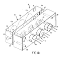
- a fiber optic array 120 having fiber optic units 100 formed in transparent substrate 106, includes additional optical features 102 adjacent to fiber optic units 100 that are used to produce fiducial marks 104 on the treated portion 107 of opposing surface 106b of the fiber optic array 120.
- the fiber optic units 100 may be formed in transparent substrate 106 or they may be bonded to first surface 106a. The same process, described above, for forming fiducial marks 94, 104, is used in the present embodiments of the invention.
- the fiber optic array wherein said at least two optical features comprise diffractive microlenses.
- the fiber optic array wherein said refractive microlenses comprise aspheric microlenses.
- the fiber optic array wherein said refractive microlenses comprise spheric microlenses.
- the method of manufacturing a fiber optic array wherein said step of altering includes the step of ablating said at least a portion of said second surface so as to distinguish at least two fiducial marks formed thereon.
- the method of manufacturing a fiber optic array wherein said step of forming said at least two optical features includes the step of forming said at least two optical features by diamond milling.
- the method of manufacturing a fiber optic array wherein said step of forming said at least two optical features includes the step of forming said at least two optical features by diamond turning.
- the method of manufacturing a fiber optic array wherein said step of forming said at least two optical features includes the step of forming said at least two optical features by a process of indentation.
- the method of manufacturing a fiber optic array wherein said step of altering includes the step of painting said at least a portion of said second surface so as to distinguish said at least two fiducial marks formed thereon.
- the method of manufacturing a fiber optic array wherein said step of altering includes the step of metallizing said at least a portion of said second surface so as to distinguish said at least two fiducial marks formed thereon.
- the method of manufacturing a fiber optic array wherein said step of altering includes the step of vacuum coating said at least a portion of said second surface so as to distinguish said at least two fiducial marks formed thereon.
- the method of manufacturing a fiber optic array wherein said step of altering includes the step of roughening said at least a portion of said second surface so as to distinguish said at least two fiducial marks formed thereon.
- the method of manufacturing a fiber optic array wherein said step of altering includes the step of spin coating said at least a portion of said second surface so as to distinguish said at least two fiducial marks formed thereon.
- the method of manufacturing a fiber optic array wherein said step of altering includes the step of dip coating said at least a portion of said second surface so as to distinguish said at least two fiducial marks formed thereon.
- the method of manufacturing a fiber optic array wherein said step of forming said at least two optical features on said first surface includes the step of diamond milling.
- the method of manufacturing a fiber optic array wherein said step of forming said at least two optical features on said first surface includes the step of diamond turning.
- the method of manufacturing a fiber optic array wherein said step of forming said at least two optical features on said first surface includes the step of etching.
Landscapes
- Physics & Mathematics (AREA)
- General Physics & Mathematics (AREA)
- Optics & Photonics (AREA)
- Engineering & Computer Science (AREA)
- Manufacturing & Machinery (AREA)
- Optical Couplings Of Light Guides (AREA)
- Laser Beam Processing (AREA)
Applications Claiming Priority (2)
| Application Number | Priority Date | Filing Date | Title |
|---|---|---|---|
| US27748 | 2001-12-20 | ||
| US10/027,748 US6748145B2 (en) | 2001-12-20 | 2001-12-20 | Fiber optic array and method of making same |
Publications (2)
| Publication Number | Publication Date |
|---|---|
| EP1321784A2 true EP1321784A2 (fr) | 2003-06-25 |
| EP1321784A3 EP1321784A3 (fr) | 2004-04-28 |
Family
ID=21839557
Family Applications (1)
| Application Number | Title | Priority Date | Filing Date |
|---|---|---|---|
| EP02080197A Withdrawn EP1321784A3 (fr) | 2001-12-20 | 2002-12-09 | Connecteur d'ensemble de fibres optiques et procédé de fabrication de marques d'ajustage |
Country Status (3)
| Country | Link |
|---|---|
| US (1) | US6748145B2 (fr) |
| EP (1) | EP1321784A3 (fr) |
| JP (1) | JP2003200278A (fr) |
Cited By (2)
| Publication number | Priority date | Publication date | Assignee | Title |
|---|---|---|---|---|
| WO2012015471A1 (fr) * | 2010-07-30 | 2012-02-02 | Tyco Electronics Corporation | Corps ayant une lentille couplée pour réaliser une image d'un élément d'alignement |
| US8977088B2 (en) | 2010-07-30 | 2015-03-10 | Tyco-Electronics Corporation | Interposer with alignment features |
Families Citing this family (11)
| Publication number | Priority date | Publication date | Assignee | Title |
|---|---|---|---|---|
| US6683723B2 (en) * | 2002-06-13 | 2004-01-27 | Eastman Kodak Company | Solid immersion lens array and methods for producing and using solid immersion lens array with fiducial marks |
| US20100183266A1 (en) * | 2007-06-14 | 2010-07-22 | Kazuya Shimoda | Optical module and method for manufacturing the same |
| JP4477677B2 (ja) | 2008-01-16 | 2010-06-09 | 古河電気工業株式会社 | 光モジュールおよびその作製方法 |
| US9063323B2 (en) | 2009-10-19 | 2015-06-23 | Pixar | Super light-field lens and image processing methods |
| US9063345B2 (en) * | 2009-10-19 | 2015-06-23 | Pixar | Super light-field lens with doublet lenslet array element |
| US9197799B2 (en) * | 2009-10-19 | 2015-11-24 | Pixar | Super light field lens with focus control and non spherical lenslet arrays |
| JP5508869B2 (ja) * | 2010-01-19 | 2014-06-04 | 日本航空電子工業株式会社 | 光コネクタ装置 |
| US8757758B2 (en) * | 2011-08-25 | 2014-06-24 | Eastman Kodak Company | Multiple sided media pattern registration system |
| TWI461775B (zh) * | 2012-09-26 | 2014-11-21 | Delta Electronics Inc | 光通訊模組及其耦光組接方法 |
| US11892701B2 (en) | 2020-04-17 | 2024-02-06 | Apple Inc. | Lens mounting structures for head-mounted devices |
| JP7381174B2 (ja) * | 2021-05-21 | 2023-11-15 | 三菱電機株式会社 | 光モジュール |
Family Cites Families (14)
| Publication number | Priority date | Publication date | Assignee | Title |
|---|---|---|---|---|
| US4598039A (en) | 1984-07-02 | 1986-07-01 | At&T Bell Laboratories | Formation of features in optical material |
| US4904087A (en) * | 1987-07-06 | 1990-02-27 | American Telephone & Telegraph Co., At&T Bell Laboratories | Method for aligning photomasks |
| US5728324A (en) * | 1995-01-31 | 1998-03-17 | Digital Optics Corporation | Molding diffractive optical elements |
| JP3405087B2 (ja) | 1995-11-06 | 2003-05-12 | ソニー株式会社 | 液晶表示装置およびその製造方法 |
| US5850276A (en) | 1995-11-06 | 1998-12-15 | Sony Corporation | Method of making LCD device having alignment mark made of same material and formed at same time as microlenses |
| JPH09311253A (ja) * | 1996-05-20 | 1997-12-02 | Fujitsu Ltd | 光結合構造とその製造方法 |
| US6005294A (en) | 1996-05-29 | 1999-12-21 | Mitsubishi Denki Kabushiki Kaisha | Method of arranging alignment marks |
| US6096155A (en) | 1996-09-27 | 2000-08-01 | Digital Optics Corporation | Method of dicing wafer level integrated multiple optical elements |
| JP3155717B2 (ja) * | 1996-10-24 | 2001-04-16 | 日本板硝子株式会社 | マイクロレンズに対するレーザ加工方法 |
| JP2001507814A (ja) * | 1996-12-31 | 2001-06-12 | ハネウエル・インコーポレーテッド | フレキシブル光コネクタアセンブリ |
| JPH11311721A (ja) * | 1998-02-27 | 1999-11-09 | Oki Electric Ind Co Ltd | 光結合モジュールおよびその製造方法 |
| US6406195B1 (en) * | 1999-10-14 | 2002-06-18 | Digital Optics Corporation | Interface between opto-electronic devices and fibers |
| US6587274B1 (en) * | 2001-12-20 | 2003-07-01 | Eastman Kodak Company | Double-sided microlens array and method of manufacturing same |
| US6515800B1 (en) * | 2001-12-20 | 2003-02-04 | Eastman Kodak Company | Microlens array |
-
2001
- 2001-12-20 US US10/027,748 patent/US6748145B2/en not_active Expired - Fee Related
-
2002
- 2002-12-09 EP EP02080197A patent/EP1321784A3/fr not_active Withdrawn
- 2002-12-19 JP JP2002368243A patent/JP2003200278A/ja active Pending
Cited By (5)
| Publication number | Priority date | Publication date | Assignee | Title |
|---|---|---|---|---|
| WO2012015471A1 (fr) * | 2010-07-30 | 2012-02-02 | Tyco Electronics Corporation | Corps ayant une lentille couplée pour réaliser une image d'un élément d'alignement |
| US8262297B2 (en) | 2010-07-30 | 2012-09-11 | Tyco Electronics Corporation | Body having a dedicated lens for imaging an alignment feature |
| CN103038685A (zh) * | 2010-07-30 | 2013-04-10 | 泰科电子公司 | 具有用于对对齐特征进行成像的专用透镜的本体 |
| CN103038685B (zh) * | 2010-07-30 | 2015-03-04 | 泰科电子公司 | 具有用于对对齐特征进行成像的专用透镜的本体 |
| US8977088B2 (en) | 2010-07-30 | 2015-03-10 | Tyco-Electronics Corporation | Interposer with alignment features |
Also Published As
| Publication number | Publication date |
|---|---|
| US20030118290A1 (en) | 2003-06-26 |
| EP1321784A3 (fr) | 2004-04-28 |
| US6748145B2 (en) | 2004-06-08 |
| JP2003200278A (ja) | 2003-07-15 |
Similar Documents
| Publication | Publication Date | Title |
|---|---|---|
| US6765603B2 (en) | Method of forming fiducial marks on a micro-sized article | |
| US6845120B2 (en) | Laser array and method of making same | |
| US6748145B2 (en) | Fiber optic array and method of making same | |
| US6587274B1 (en) | Double-sided microlens array and method of manufacturing same | |
| JP4903685B2 (ja) | 集積光学システムを製造する方法 | |
| US6104690A (en) | Integrated optical apparatus and associated methods | |
| US8153957B2 (en) | Integrated optical imaging systems including an interior space between opposing substrates and associated methods | |
| US6515800B1 (en) | Microlens array | |
| JP3889247B2 (ja) | 光モジュールおよびその組立て方法 | |
| EP1362247B1 (fr) | Compensation et/ou variation de lentilles produites sur une plaquette et structures obtenues | |
| US6594084B1 (en) | Method and manufacturing a precisely aligned microlens array | |
| US7263249B2 (en) | Optical element assembly and method of making the same | |
| EP1353205B1 (fr) | Alignement d'un assemblage de fibres utilisant des repères d'ajustage | |
| US20030174943A1 (en) | Optical devices and methods of manufacture | |
| US6379777B1 (en) | Die and production method thereof, glass substrate and production method thereof and method of forming pattern on the glass substrate | |
| US6934449B2 (en) | Optical device permitting passive alignment of lens element | |
| US20070110361A1 (en) | Wafer level integration of multiple optical elements | |
| JP4219677B2 (ja) | 光学装置の製造方法 | |
| EP0954395A1 (fr) | Micro-replication dans du metal | |
| KR100647283B1 (ko) | 마이크로 렌즈 제조 방법 | |
| US20240019609A1 (en) | Forming an optical system | |
| KR20000027810A (ko) | 반도체기판의 초점인식 정렬장치 및 그 방법 |
Legal Events
| Date | Code | Title | Description |
|---|---|---|---|
| PUAI | Public reference made under article 153(3) epc to a published international application that has entered the european phase |
Free format text: ORIGINAL CODE: 0009012 |
|
| AK | Designated contracting states |
Designated state(s): AT BE BG CH CY CZ DE DK EE ES FI FR GB GR IE IT LI LU MC NL PT SE SI SK TR |
|
| AX | Request for extension of the european patent |
Extension state: AL LT LV MK RO |
|
| PUAL | Search report despatched |
Free format text: ORIGINAL CODE: 0009013 |
|
| RIC1 | Information provided on ipc code assigned before grant |
Ipc: 7G 02B 6/36 B Ipc: 7G 02B 6/32 A |
|
| AK | Designated contracting states |
Kind code of ref document: A3 Designated state(s): AT BE BG CH CY CZ DE DK EE ES FI FR GB GR IE IT LI LU MC NL PT SE SI SK TR |
|
| AX | Request for extension of the european patent |
Extension state: AL LT LV MK RO |
|
| 17P | Request for examination filed |
Effective date: 20040913 |
|
| 17Q | First examination report despatched |
Effective date: 20041005 |
|
| AKX | Designation fees paid |
Designated state(s): DE |
|
| STAA | Information on the status of an ep patent application or granted ep patent |
Free format text: STATUS: THE APPLICATION IS DEEMED TO BE WITHDRAWN |
|
| 18D | Application deemed to be withdrawn |
Effective date: 20050216 |