EP1321969B1 - Procédé et dispositif de manipulation de plaquettes semiconductrices - Google Patents
Procédé et dispositif de manipulation de plaquettes semiconductrices Download PDFInfo
- Publication number
- EP1321969B1 EP1321969B1 EP02026853A EP02026853A EP1321969B1 EP 1321969 B1 EP1321969 B1 EP 1321969B1 EP 02026853 A EP02026853 A EP 02026853A EP 02026853 A EP02026853 A EP 02026853A EP 1321969 B1 EP1321969 B1 EP 1321969B1
- Authority
- EP
- European Patent Office
- Prior art keywords
- wafer
- sensors
- chuck
- nozzles
- vacuum
- Prior art date
- Legal status (The legal status is an assumption and is not a legal conclusion. Google has not performed a legal analysis and makes no representation as to the accuracy of the status listed.)
- Expired - Lifetime
Links
Images
Classifications
-
- H—ELECTRICITY
- H10—SEMICONDUCTOR DEVICES; ELECTRIC SOLID-STATE DEVICES NOT OTHERWISE PROVIDED FOR
- H10P—GENERIC PROCESSES OR APPARATUS FOR THE MANUFACTURE OR TREATMENT OF DEVICES COVERED BY CLASS H10
- H10P72/00—Handling or holding of wafers, substrates or devices during manufacture or treatment thereof
- H10P72/06—Apparatus for monitoring, sorting, marking, testing or measuring
- H10P72/0606—Position monitoring, e.g. misposition detection or presence detection
-
- H—ELECTRICITY
- H10—SEMICONDUCTOR DEVICES; ELECTRIC SOLID-STATE DEVICES NOT OTHERWISE PROVIDED FOR
- H10P—GENERIC PROCESSES OR APPARATUS FOR THE MANUFACTURE OR TREATMENT OF DEVICES COVERED BY CLASS H10
- H10P72/00—Handling or holding of wafers, substrates or devices during manufacture or treatment thereof
- H10P72/50—Handling or holding of wafers, substrates or devices during manufacture or treatment thereof for positioning, orientation or alignment
- H10P72/53—Handling or holding of wafers, substrates or devices during manufacture or treatment thereof for positioning, orientation or alignment using optical controlling means
-
- H—ELECTRICITY
- H10—SEMICONDUCTOR DEVICES; ELECTRIC SOLID-STATE DEVICES NOT OTHERWISE PROVIDED FOR
- H10P—GENERIC PROCESSES OR APPARATUS FOR THE MANUFACTURE OR TREATMENT OF DEVICES COVERED BY CLASS H10
- H10P72/00—Handling or holding of wafers, substrates or devices during manufacture or treatment thereof
- H10P72/70—Handling or holding of wafers, substrates or devices during manufacture or treatment thereof for supporting or gripping
- H10P72/78—Handling or holding of wafers, substrates or devices during manufacture or treatment thereof for supporting or gripping using vacuum or suction, e.g. Bernoulli chucks
Definitions
- the present invention relates to a method and a Device for handling plates, in particular semiconductor wafers, to record in a first place and in their situation to change or to transport to a second place are.
- Semiconductor wafers or wafers are known to be very thin and have a diameter of the order of 2 to 8 Inch thicknesses on the order of a few 10 to a few 100 microns.
- Such semiconductor wafers are so far mostly manually or with a handling system of a first processing location to a second processing location brought.
- a handling system of a first processing location to a second processing location brought.
- These wafers can be processed by the handling system no longer be handled problem-free. Therefore, be They are generally made manually with the help of tweezers taken appropriate container and for further processing For example, brought in a so-called quartz boat.
- a quartz boat is a particular storage case for Semiconductor wafers.
- the use of tweezers is not unproblematic, since this easily to partial damage, like the formation of hairline cracks and therefore one Failure of chips in the corresponding area of the semiconductor wafer can lead.
- WO99 / 17244 discloses a gripping device for vacuum-assisted Holding a semiconductor wafer.
- the gripping device is designed in several parts and has nozzle holes for vacuum bracket.
- a rotatable holder disclosed that a semiconductor slice to Uussgabe from sensor signals to a predetermined position.
- robot conventional handling machine
- This task is accomplished by a procedure with the characteristics of the Claim 1 solved.
- the holding device is in several parts is executed and at least in the center nozzle holes for hydrodynamically holding the semiconductor wafer, and when centering for centering the aligning Semiconductor disk are present, which further nozzle holes for generating a center outward hydrodynamic negative pressure and diametrically movable centering bevels and if further the center of one rotatable holder is formed, with the help of which to handling semiconductor wafer in accordance with sensor signals can be moved in a predeterminable position.
- the rotatable holder is a chuck, which Both vacuum nozzles and Bernoullidüsen, let to simplify the centering and clamping operations and optimize, it is equally advantageous whether now the feed through a worm gear or through a Belt transmission is driven.
- the holding device centering slopes, which the feed (Chuck) diametrically partially encompass and by means of a Joint gear apart and can be moved together, wherein the linkage by a lifting cylinder and a Push rod is formed.
- the automatic is supported Centering through the concentric arrangement of Bernoulli nozzles in the feed (chuck).
- sensor signals are spatially separated by at least two generates spaced sensors, which as sensors the edge position can detect a flattening of the semiconductor wafer.
- This flattening - also called “flat” - serves the clear Position assignment of the semiconductor wafer. If all the semiconductor wafers are aligned so that all flats exactly the the same position to each other, is the positioning of the Semiconductors correct.
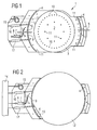
- a gripping device 1 shown in Figure 1 consists of several parts that are relatively movable.
- a rotatable holder 3 which is the Recording of semiconductor wafers is used.
- the rotatable holder 3 partially enclosed by centering 4.
- These centering bevels 4 are arranged diametrically and can be in a diametrical direction towards each other and Move away from each other, which by directional arrows 5 and 6 is hinted at.
- the push rod 9 shown continuously in this figure the position in which the centering bevels 4 in their centering position.
- nozzle openings are arranged, which produce the so-called Bernoulli effect and as so-called Bernoullidüsen 11 for carrying the male Serve semiconductor wafer.
- the rotatable holder 3 are arranged concentrically in an outer circle vacuum nozzles 10, which serve to fix the semiconductor wafer and separated from the Bernoullidüsen 11 at the periphery of Centering bevel 4 can be activated.
- an inner one Circle are also arranged concentrically further nozzle openings, which also the so-called Bernoulli effect generate and therefore also referred to as Bernoullidüsen 11 become.
- the Bernoulli jets 11 are oblique from the inner center 2 outwardly directed bores, through which a fluid, For example, air or another gas is passed.
- a fluid For example, air or another gas is passed.
- This Fluid causes a flow, which accordingly to the outside is directed and for a thin wafer wafer a kind of floating layer generated by which the thin wafer disk is leveled and on which they hover relatively stable will be carried.
- Vacuum nozzles 10 With simultaneous activation of the mentioned Vacuum nozzles 10, the position of the wafer wafer in addition stabilized.
- the centering bevels 4 serve to center the wafer wafer, by the joint action of the Bernoulli effect and vacuum the wafer slice over the oblique Areas of the centering bevels 4, the wafer disk to the center. 2 the gripping device 1 is pulled.
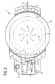
- the arrangement of a wafer wafer 12 shown in FIG on a gripping device 1 according to the invention makes a situation clearly, which the steps a. and b. of the first Claim corresponds.
- the arrangement consisting of gripping device 1 and wafer disk 12 is in the automatic Wafer handling still in the aforementioned Material carrier, such as a horde, not shown.
- a next step which corresponds to step c. of the claim 1, essentially only the negative pressure acts through the vacuum nozzles 10 in the rotatable holder 3 and the air of the Bernoulli nozzles 11 in the rotatable holder 3 and supported on the periphery of the centering 4 the wafer wafer 12.
- the wafer wafer 12 is characterized on the rotatable holder 3 fixed, the centering be 4 according to step d. drove apart and give the scope the wafer wafer 12 free, the Bernoullidüsen 11 the Friction between the centering bevels 4 and the wafer disk 12 further reduce.
- the wafer disk 12 is therefore up the vacuum-related fixation on the rotatable holder 3 completely free and located in relation to a flattening (Flat) 13 on the circumference of the wafer wafer 12 in an undefined Position relative to the gripping device 1.
- Controlled by a control unit 14 is in accordance with a Program the rotatable holder 3 by means of a belt drive 15 (see also Figure 1) rotated, the rotation is detected by sensors 16 and 17, which the flattening 13th at the periphery of the wafer disk 12 detect.
- the control unit 14 gives a control command according to his control program to the belt drive 15 and the rotational speed of the holder 3 with the wafer 12 is reduced so much that at Detecting the flat 13 of the wafer 12 by the second Sensor 17 or 16, the wafer rotation is stopped. This happens due to another signal, which from the corresponding Transmit sensor 17 or 16 to the control unit 14 is, which in turn in a conventional manner a stop signal generates the rotating bracket 3 and thus the wafer 12 is stopped.
- Target position The wafer 12 is now in its desired position, which can be referred to as "target position". These Target position of the wafer 12 is in the illustration in FIG. 3 shown. In this constellation, the wafer 12 is using the gripping device 1 according to feature step h. of the claim 1 back to his aforementioned, but not explicitly shown Horde transported. Of course he can too be stored at any other desired location. In any case he is in this constellation both in terms of its nominal position as well as regarding his evenness for the others Processing steps ready vorbreitet.
Landscapes
- Container, Conveyance, Adherence, Positioning, Of Wafer (AREA)
Claims (14)
- Procédé pour manipuler automatiquement des plaquettes minces, en particulier des tranches minces, lors du chargement ou du déchargement sur des porte-matériau à l'aide d'un système automatique de manipulation ; le procédé comprend les étapes suivantes :a) un dispositif de préhension (1) se déplace sensiblement parallèlement à une plaquette (12) dans le porte-matériau,b) par des moyens pneumatiques, la plaquette (12) est aplanie et elle est centrée dans le dispositif de préhension (1) par des éléments de centrage (4, 11),c) la plaquette (12) dans le dispositif de préhension (1) est immobilisée sur un support (3) à l'aide du vide,d) les éléments de centrage (4, 11) sont détachés de la plaquette (12),e) la plaquette (12) est tournée à l'aide du support (3),f) la position de la plaquette (12) est détectée par des détecteurs (16, 17),g) la rotation de la plaquette (12) est arrêtée lorsqu'elle atteint une position prédéterminable,h) la plaquette (12), aplanie et exactement placée, est déposée dans un porte-matériau de type quelconque.
- Procédé selon la revendication 1, caractérisé en ce que la rotation de la plaquette (12) est détectée par plusieurs détecteurs (16, 17) conçus sous forme de palpeurs.
- Procédé selon la revendication 1 ou 2, caractérisé en ce que la rotation de la plaquette (12) a lieu à des vitesses différentes, la vitesse dépendant de signaux des détecteurs (16, 17).
- Dispositif pour exécuter le procédé selon l'une des revendications précédentes à l'aide d'un dispositif porteur destiné à manipuler une plaquette, en particulier à l'aide d'un dispositif de préhension ; le dispositif comporte plusieurs parties et, au moins au centre (2), présente des perçages de buse (10) destinés à supporter de façon hydrodynamique une plaquette semi-conductrice (12) et dont le centre (2) est formé par un support tournant à l'aide duquel la plaquette semi-conductrice (12) à manipuler peut être déplacée dans une position prédéterminable d'après les indications des signaux de détections, caractérisé en ce qu'il existe des éléments de centrage (4, 11) qui servent à orienter de façon centrée la plaquette semi-conductrice (12) et qui comprennent d'autres perçages de buse (11) destinés à produire une dépression orientée du centre vers l'extérieur et des inclinaisons de centrage (4) mobiles et diamétralement opposées.
- Dispositif selon la revendication 4, caractérisé en ce que le support (3) tournant est un mandrin muni aussi bien de buses à vide (10) que de buses de Bernoulli (11).
- Dispositif selon la revendication 4, caractérisé en ce que le mandrin (3) peut être entraíné par un engrenage à vis sans fin.
- Dispositif selon la revendication 4, caractérisé en ce que le mandrin (3) peut être entraíné par un mécanisme à courroie (15).
- Dispositif selon la revendication 4, caractérisé en ce que les inclinaisons de centrage (4) entourent en partie diamétralement le mandrin (3) et peuvent être écartées et rassemblées à l'aide d'un mécanisme articulé (7).
- Dispositif selon la revendication 4, caractérisé en ce que le mécanisme articulé (7) est formé par un vérin de levage (8) et par une bielle (9).
- Dispositif selon la revendication 9, caractérisé en ce que le vérin de levage (8) est un vérin pneumatique.
- Dispositif selon la revendication 4, caractérisé en ce que les signaux de détection sont produits par au moins deux palpeurs, à distance l'une de l'autre, qui en tant que détecteurs (16, 17) peuvent détecter la façon dont sont placées les arêtes d'un aplatissement (13) de la plaquette semi-conductrice (12).
- Dispositif selon la revendication 4, caractérisé en ce que les buses à vide (10) et les buses de Bernoulli (11) peuvent être alimentées séparément par un fluide.
- Dispositif selon la revendication 4, caractérisé en ce que les buses à vide (10) et les buses de Bernoulli (11) sont alimentées en fluide, les inclinaisons de centrage (4) ont des mouvements relatifs, le mandrin (3) tourne et la plaquette semi-conductrice (12) est disposée selon les indications des signaux des détecteurs (16, 17) au moyen d'une unité de commande (14) qui fonctionne d'après un programme qu'on peut librement prédéfinir.
- Dispositif selon la revendication 4, caractérisé en ce que le dispositif de préhension (1) peut être intégré dans un appareil automatique de manipulation.
Applications Claiming Priority (2)
| Application Number | Priority Date | Filing Date | Title |
|---|---|---|---|
| DE10161902A DE10161902B4 (de) | 2001-12-17 | 2001-12-17 | Verfahren und Vorrichtung zum Handhaben von Platten |
| DE10161902 | 2001-12-17 |
Publications (3)
| Publication Number | Publication Date |
|---|---|
| EP1321969A2 EP1321969A2 (fr) | 2003-06-25 |
| EP1321969A3 EP1321969A3 (fr) | 2003-12-17 |
| EP1321969B1 true EP1321969B1 (fr) | 2005-03-02 |
Family
ID=7709500
Family Applications (1)
| Application Number | Title | Priority Date | Filing Date |
|---|---|---|---|
| EP02026853A Expired - Lifetime EP1321969B1 (fr) | 2001-12-17 | 2002-11-30 | Procédé et dispositif de manipulation de plaquettes semiconductrices |
Country Status (2)
| Country | Link |
|---|---|
| EP (1) | EP1321969B1 (fr) |
| DE (1) | DE10161902B4 (fr) |
Cited By (1)
| Publication number | Priority date | Publication date | Assignee | Title |
|---|---|---|---|---|
| DE102008045257A1 (de) * | 2008-09-01 | 2010-03-04 | Rena Gmbh | Vorrichtung und Verfahren zum Handhaben von Substraten |
Families Citing this family (4)
| Publication number | Priority date | Publication date | Assignee | Title |
|---|---|---|---|---|
| DE102005000665B4 (de) * | 2005-01-04 | 2009-05-20 | Nanophotonics Ag | Greifer zum Halten und Positionieren eines scheiben- oder plattenförmigen Objekts und Verfahren zum Halten und Positionieren eines scheiben- oder plattenförmigen Objekts |
| EP2843695B9 (fr) | 2013-08-28 | 2021-04-14 | Mechatronic Systemtechnik GmbH | Dispositif, notamment effecteur terminal |
| DE102019112318B3 (de) | 2019-05-10 | 2020-07-23 | Witrins S.R.O. | Vakuumspannvorrichtung |
| WO2024210830A1 (fr) * | 2023-04-06 | 2024-10-10 | PTW Asia Pte Ltd | Système et procédé de manipulation sans contact de tranches de semi-conducteur |
Family Cites Families (8)
| Publication number | Priority date | Publication date | Assignee | Title |
|---|---|---|---|---|
| US3930684A (en) * | 1971-06-22 | 1976-01-06 | Lasch Jr Cecil A | Automatic wafer feeding and pre-alignment apparatus and method |
| US3960277A (en) * | 1974-09-30 | 1976-06-01 | Flint Alan G | Mask plate handling apparatus |
| JP2806431B2 (ja) * | 1989-04-28 | 1998-09-30 | 株式会社ニデック | ウェーハ搬送装置 |
| US6002840A (en) * | 1997-09-30 | 1999-12-14 | Brooks Automation Inc. | Substrate transport apparatus |
| KR100292612B1 (ko) * | 1997-12-08 | 2001-08-07 | 윤종용 | 반도체 웨이퍼 정렬시스템 및 이를 이용하는 웨이퍼 정렬방법 |
| US6095582A (en) * | 1998-03-11 | 2000-08-01 | Trusi Technologies, Llc | Article holders and holding methods |
| JP4283926B2 (ja) * | 1999-02-22 | 2009-06-24 | 株式会社アルバック | ウエハカセットのウエハ保持システム |
| DE19948572A1 (de) * | 1999-10-08 | 2001-04-19 | Infineon Technologies Ag | Vorrichtung zum Handling von Halbleiterscheiben |
-
2001
- 2001-12-17 DE DE10161902A patent/DE10161902B4/de not_active Expired - Fee Related
-
2002
- 2002-11-30 EP EP02026853A patent/EP1321969B1/fr not_active Expired - Lifetime
Cited By (1)
| Publication number | Priority date | Publication date | Assignee | Title |
|---|---|---|---|---|
| DE102008045257A1 (de) * | 2008-09-01 | 2010-03-04 | Rena Gmbh | Vorrichtung und Verfahren zum Handhaben von Substraten |
Also Published As
| Publication number | Publication date |
|---|---|
| DE10161902A1 (de) | 2003-07-10 |
| DE10161902B4 (de) | 2005-06-23 |
| EP1321969A3 (fr) | 2003-12-17 |
| EP1321969A2 (fr) | 2003-06-25 |
Similar Documents
| Publication | Publication Date | Title |
|---|---|---|
| DE69420616T2 (de) | Aufnahme- und Fördereinheit für Stapel von Zuschnitten | |
| DE3915038C2 (fr) | ||
| DE19755694C2 (de) | Handhabungsvorrichtung für dünne, scheibenförmige Gegenstände | |
| DE60313279T2 (de) | Transportsystem | |
| DE4031163A1 (de) | Kanten-poliergeraet | |
| DE102005057173B4 (de) | Teilungseinrichtung für ein rechteckförmiges Substrat | |
| DE102010008975B4 (de) | Werkstückbearbeitungsverfahren und -vorrichtung | |
| WO2008003502A1 (fr) | Dispositif et procédé pour individualiser et transporter des substrats | |
| DE102016200272A1 (de) | Fördervorrichtung | |
| DE112006002063T5 (de) | Folienschneidvorrichtung und Folienschneidverfahren | |
| CH697146A5 (de) | Greifvorrichtung zur Handhabung von Wafern. | |
| DE3854893T2 (de) | Verfahren und Vorrichtung zum Abschrägen der Kerbe eines Halbleiterplättchen | |
| EP1321969B1 (fr) | Procédé et dispositif de manipulation de plaquettes semiconductrices | |
| DE3607561A1 (de) | Ueberfuehr- und beschickungsvorrichtung fuer wabenfoermige produkte | |
| DE102004001350A1 (de) | Förder-bzw. Transportvorrichtung für ein plattenartiges Werkstück | |
| DE102021214707B4 (de) | Bandanbringer zum anbringen eines bands an einem ringrahmen und einem wafer | |
| EP0609489B1 (fr) | Dispositif pour appliquer un masque sur un substrat et/ou pour l'enlever | |
| DE102022208122A1 (de) | Folien-anhaftvorrichtung | |
| DE102006059809B4 (de) | Vorrichtung und Verfahren zum Vereinzeln und Transportieren von Substraten | |
| DE3213923A1 (de) | Beschickungs- und wendevorrichtung fuer rotationssymmetrische teile | |
| DE102004003455B4 (de) | Verfahren und Vorrichtung zum Aufbrechen und Belüften von blattartigen Materialstapeln, insbesondere von Papierstapeln | |
| EP1935599B1 (fr) | Dispositif et procédé pour la séparation et le transport de substrats | |
| EP1445792B1 (fr) | Dispositif de manipulation de plaques | |
| EP1294014B1 (fr) | Dispositif de manipulation de plaques | |
| DE10144409B4 (de) | Vorrichtung mit einem Greifer zur Handhabung von Platten |
Legal Events
| Date | Code | Title | Description |
|---|---|---|---|
| PUAI | Public reference made under article 153(3) epc to a published international application that has entered the european phase |
Free format text: ORIGINAL CODE: 0009012 |
|
| AK | Designated contracting states |
Designated state(s): AT BE BG CH CY CZ DE DK EE ES FI FR GB GR IE IT LI LU MC NL PT SE SK TR |
|
| AX | Request for extension of the european patent |
Extension state: AL LT LV MK RO SI |
|
| PUAL | Search report despatched |
Free format text: ORIGINAL CODE: 0009013 |
|
| AK | Designated contracting states |
Kind code of ref document: A3 Designated state(s): AT BE BG CH CY CZ DE DK EE ES FI FR GB GR IE IT LI LU MC NL PT SE SK TR |
|
| AX | Request for extension of the european patent |
Extension state: AL LT LV MK RO SI |
|
| 17P | Request for examination filed |
Effective date: 20040525 |
|
| GRAP | Despatch of communication of intention to grant a patent |
Free format text: ORIGINAL CODE: EPIDOSNIGR1 |
|
| AKX | Designation fees paid |
Designated state(s): FR GB |
|
| REG | Reference to a national code |
Ref country code: DE Ref legal event code: 8566 |
|
| GRAS | Grant fee paid |
Free format text: ORIGINAL CODE: EPIDOSNIGR3 |
|
| GRAA | (expected) grant |
Free format text: ORIGINAL CODE: 0009210 |
|
| AK | Designated contracting states |
Kind code of ref document: B1 Designated state(s): FR GB |
|
| REG | Reference to a national code |
Ref country code: GB Ref legal event code: FG4D Free format text: NOT ENGLISH |
|
| REG | Reference to a national code |
Ref country code: IE Ref legal event code: FG4D Free format text: GERMAN |
|
| GBT | Gb: translation of ep patent filed (gb section 77(6)(a)/1977) |
Effective date: 20050504 |
|
| PLBE | No opposition filed within time limit |
Free format text: ORIGINAL CODE: 0009261 |
|
| STAA | Information on the status of an ep patent application or granted ep patent |
Free format text: STATUS: NO OPPOSITION FILED WITHIN TIME LIMIT |
|
| ET | Fr: translation filed | ||
| 26N | No opposition filed |
Effective date: 20051205 |
|
| REG | Reference to a national code |
Ref country code: FR Ref legal event code: PLFP Year of fee payment: 14 |
|
| REG | Reference to a national code |
Ref country code: FR Ref legal event code: PLFP Year of fee payment: 15 |
|
| REG | Reference to a national code |
Ref country code: FR Ref legal event code: PLFP Year of fee payment: 16 |
|
| PGFP | Annual fee paid to national office [announced via postgrant information from national office to epo] |
Ref country code: FR Payment date: 20171121 Year of fee payment: 16 |
|
| PGFP | Annual fee paid to national office [announced via postgrant information from national office to epo] |
Ref country code: GB Payment date: 20171123 Year of fee payment: 16 |
|
| GBPC | Gb: european patent ceased through non-payment of renewal fee |
Effective date: 20181130 |
|
| PG25 | Lapsed in a contracting state [announced via postgrant information from national office to epo] |
Ref country code: FR Free format text: LAPSE BECAUSE OF NON-PAYMENT OF DUE FEES Effective date: 20181130 |
|
| PG25 | Lapsed in a contracting state [announced via postgrant information from national office to epo] |
Ref country code: GB Free format text: LAPSE BECAUSE OF NON-PAYMENT OF DUE FEES Effective date: 20181130 |